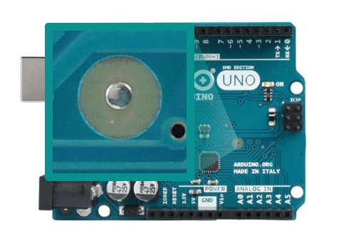
In the past, I’ve always seen small circuits of copper with no silk screen or solder mask on top of it and as a PCB designer I have always the question in my mind: What is it for? — I’ve never needed them before!
As I can find them in Arduino’s PCBs as well, I decided to open the design file and investigate more about these marks. They are called: Fiducial marks.
Fiducial Mark is a circuit solder mask with a round bare copper in the center. The copper diameter is smaller than the solder mask. As the name may imply; these marks are used by assembling machines as points of reference, and they should be placed in any PCB side that has SMD components.
No restrict rule about how many or where theses marks should be placed. But according to the reference, it’s good to position two fiducial marks on opposite corners of the PCB, and it’s advisable to put a mark near the packages with small pitch like BGA, QFN and QFP.
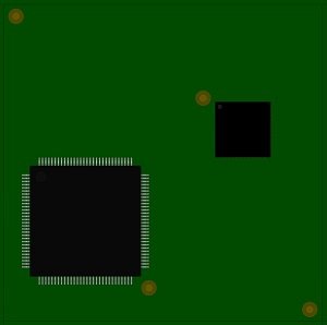
When it comes to size of fiducial marks, it depends on the used assembly machine. The mark dimensions could be 3.2mm of solder mask opening diameter and 1.6mm diameter of bare copper or 2mm of solder mask opening diameter and 1mm diameter of bare copper.
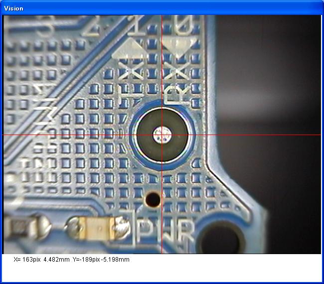
I found a video on Youtube showing how Fiducial Marks are recognized in a PnP (Pick and Place) machine.
Also, I found that Ladyada made a short blog post on the problems you may face using Fiducial Marks recognition in PnPs.


