120 Seconds Voice Record – Play Back
- Rajkumar Sharma
- 13.638 Views
- medium
- Tested
- SKU: EL34127
- Quote Now
- 0 Likes


This project is a message recording board capable of recording 120 secs of audio.
Description
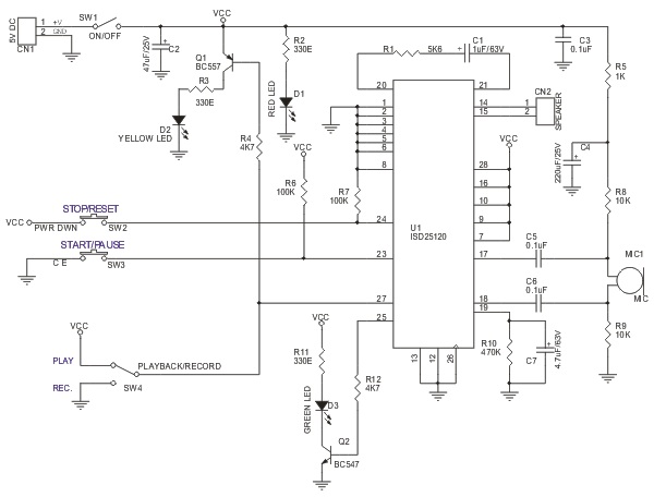
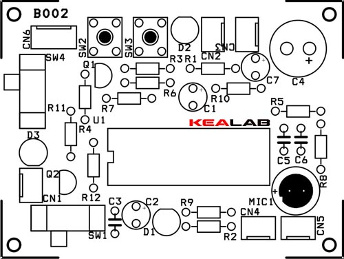
This project is designed around ISD25120 which can store 120 Seconds audio. Recording and playback operations are controlled with tact switches. The kit has an onboard microphone and LED to indicate the functions of Play and Recording. IC has a re recordable non-volatile memory which means that the message will be stored even after the units are turned off and even when it is turned on again.
Specifications:
- Input supply – 5 VDC @ 120 mA
- Output – speaker, 16 Ω
- Upto 120 Seconds of non volatile voice storage
- Slide switch for easy selection of Playback / Record mode
- Onboard MIC capsule for recording message directly onto the chip
- Flashing LED to display Record / Playback of messages
- ON Board ON/OFF Switch
- Power-On LED indicator
- Direct speaker connection via Header Connector
- Header type connector for power supply input
- 4 pin small tactile switches for Start / Pause and Stop / Reset
- Four mounting holes of 3.2 mm each
Schematic
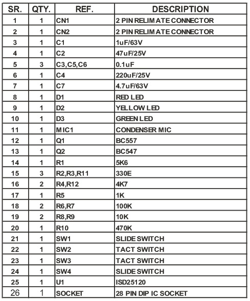
Parts List
Please follow and like us:
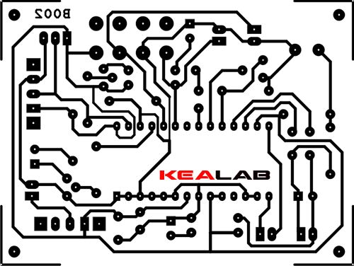
PCB


Subscribe
Login
0 Comments