

Mini Audio Amplifier
- Rajkumar Sharma
- 14.681 Views
- moderate
- Tested
- SKU: EL34276
- Quote Now
- 0 Likes

This project is a mini Audio Amplifier based on LM386 IC.
Description
The Mini Audio Amplifier project is a good choice for battery operated gadgets. It is based on Texas instruments LM386 IC, provides high quality Audio.
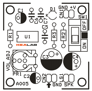
Specifications
- Wide power supply input 6 to 12 VDC
- 500 mW output @ 8 Ohms load
- Takes standard audio signal as input
- Low quiescent current drain 4 mA IC
- The quiescent power drain is only 24 mW when operating from 6 VDC
- Onboard preset for volume adjust
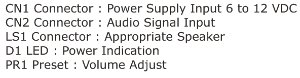
- Header connector for connecting power supply, audio signal and speaker
- Onboard power indication LED
- On/Off PCB mounted slide switch for power supply
- Four mounting holes of 3.2 mm each
- PCB dimensions 41 mm x 41 mm
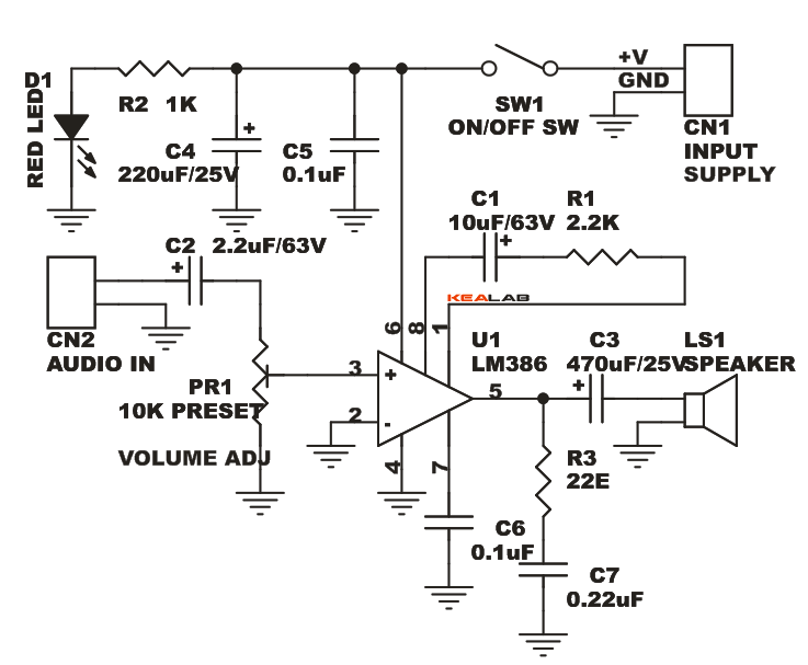
Schematic
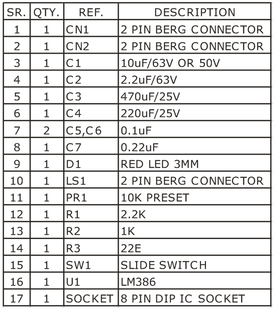
Parts List
Please follow and like us:
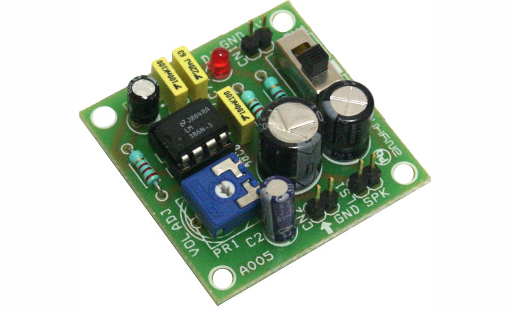
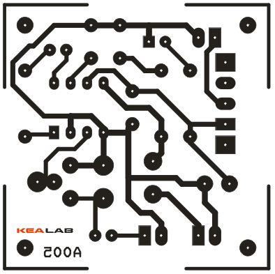
PCB


The LM358 has crossover distortion and is too noisy for audio.
The inverting opamp circuit shorts away most of the signal from the mic, it should be non-inverting with a much higher input resistance.