
Learning Board for Microchip PIC12F683 microcontroller
- Rajendra Bhatt
- rajbex@yahoo.com
- 21.866 Views
- medium
- Tested
- 0 Likes

Introduction
Electronics is my hobby. When I was in college I had some experience with microcontrollers; I did few projects with Atmel’s AT89C51. Recently, I have grown interest on PIC microcontrollers, and I thought I should start with 8-pin microchips. I picked PIC12F683 microchip. This microcontroller fascinated me a lot because I wanted to see what we can do with an 8-pin microcontroller (out of which 2 pins goes to power supply, so actually just 6-pins are left for I/O). So I thought of making my own learning board for this. In this project, I am first going to describe the learning board that I made, and then will demonstrate few experiments on it.
Some of the features of PIC12F683:
- Wide operating voltage range (2.0-5.5V)
- Precision internal oscillator (software selectable, 8 MHz to 125 Khz)
- 6 I/O pins with interrupt-on-change features.
- Four 10-bit A/D converters
- Two 8-bit and one 16-bit timers
- One Capture, Compare, PWM module
- In-Circuit Serial Programming
- Program Memory- 2048 words, SRAM- 128 bytes, EEPROM-256 bytes
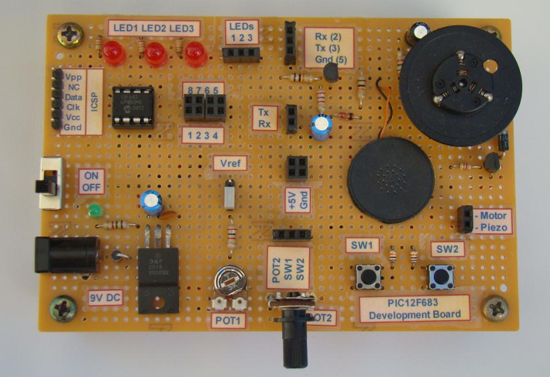
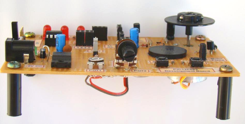
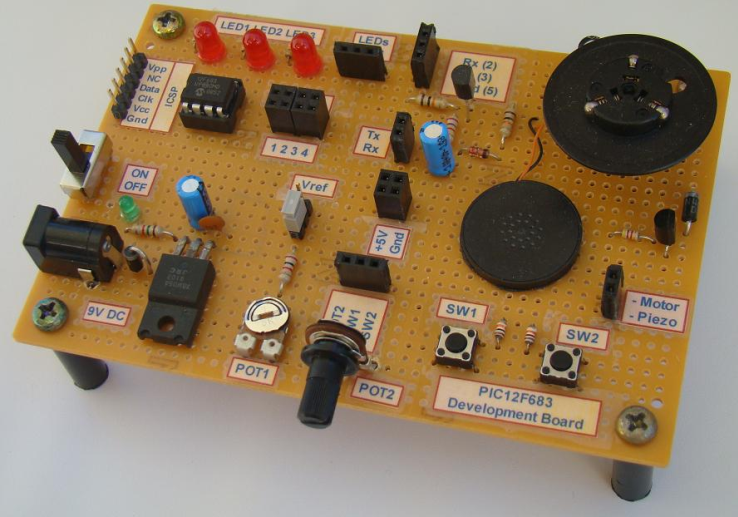
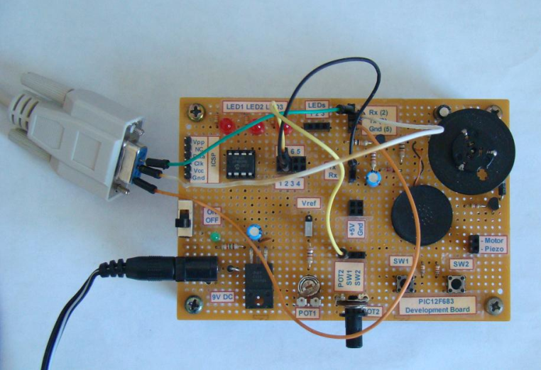
Circuit Layout and Design
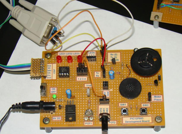
This learning board has the following features:
- A 9V DC input socket with power on switch
- Regulated +5V power supply using 7805 IC
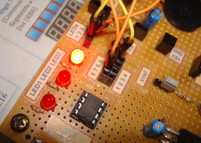
- 3 output LEDs and 1 power on LED
- 2 input tact switches
- 2 potentiometers: one for analog input and the other for providing reference voltage for ADC
- Transistor-based TTL-RS232 level converter for serial communication.
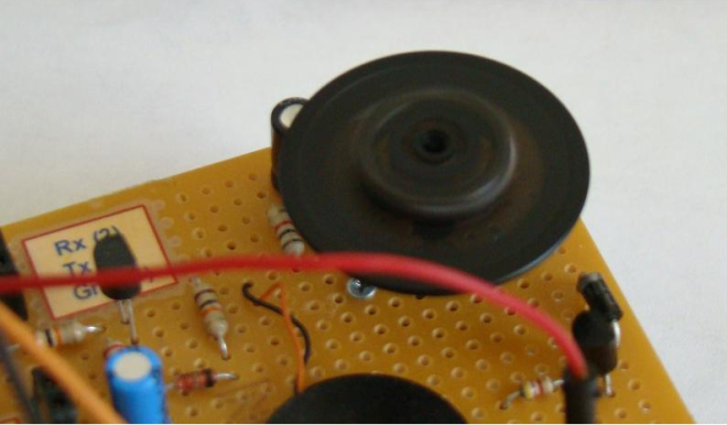
- A DC motor with a transistor driver.
- A piezo-buzzer
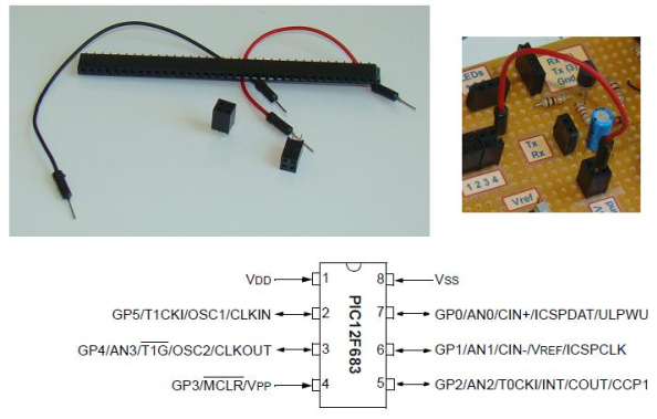
Most of these features on the board are accessible through female header pins. None of the 6-I/O pins of PIC12F683 are hardwired to anything and they are accessible through header pins too. The figures below show PIC12F683 pins, the type of female headers and jumpers used to make connection on the board, and the detail circuit diagram of the learning board. Only the ISCP pins are accessible through male header pins. The entire circuit is built on a 8 x 12 cm general prototyping board.
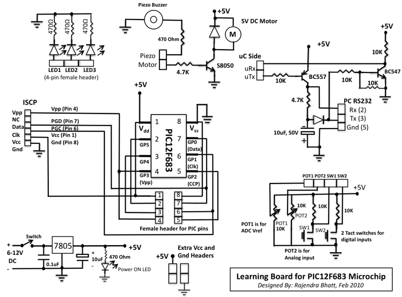
As you see the output LEDs have 470Ω current limiting resistors in series so that a PIC pin can be safely drive them. The piezo buzzer is also driven directly by a PIC pin through a series resistor. The DC motor, however, is connected as a load to the collector of S8050 transistor as the required current to drive the motor cannot be supplied by the PIC port. So, the PIC port can switch on the transistor by pulling its base HIGH and the collector current of the transistor provides the sufficient current to drive the motor.
The TTL to RS232 level converter and vice-versa is achieved with two transistors and few other components. The negative voltage required for RS232 level is stolen from the RS232 port of a PC itself. Note that there is no hardware UART inside PIC12F683, so the serial data transfer from the microcontroller to PC will be possible only through a software UART through any of GP0, GP1, GP2, GP4, and GP5 ports (GP3 is input only). The transmitter and receiver port on microcontroller side are denoted by uTx and uRx, whereas on the PC side are denoted by Tx and Rx, respectively.
The circuit diagram shows that the two input tact switches with the two potentiometer outputs and all the eight PIC12F683 pins are accessible through female headers. The tact switches are active low, i.e., under normal condition, a tact switch output is HIGH and when it is pressed, the output is LOW. There are couple of extra headers for Vcc and Gnd terminals which may be required while doing experiments.
he power supply circuit is the standard circuit of 7805 regulator IC. A power-on LED is connected across Vcc and Gnd with a 470Ω series resistor.
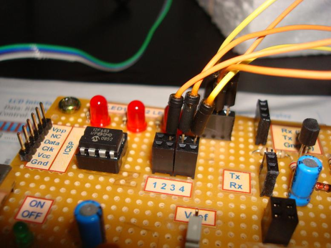
The in-circuit serial programming (ICSP) of PIC12F683 can be done with two pins: ICSPDAT (pin 7), and ICSPCLK (pin 6). The programming voltage, Vpp, should be provided to pin 4 of PIC12F683 while programming. All the required ISCP pins are available through a male header, so the PIC can be programmed through any ICSP PIC programmer. Make sure that the sequence of ISCP pins on the programmer side and our learning board match.
During ICSP, pins 4, 6, and 7 of PIC12F683 should not be connected to anything; leave them open so that there won’t be any voltage conflict between the programmer and the external circuit.
Software Development
You can write your experimental programs for PIC12F683 in assembly or high level language. But for the experiments that I am going to demonstrate here, I am using the free version of mikroC compiler from MikroElektronica. It is a C compiler for PIC microchips, and the free version limits output program size to 2K. But we don’t need more than that for PIC12F683.
We will use the following configuration bits for PIC12F683. In mikroC, you can select these in Edit Project window.
Oscillator : Internal RC, No Clock
WDT OFF
Master Clear Disabled
For all the experiments demonstrated here, use internal clock at 4.0 MHz.
Completed Learning Board for PIC12F683
Test Experiments
Read once again the Software Development section above before proceeding.
Experiment No. 1: 3-bit Binary UP Counter
The objective of this experiment is to build a 3-bit binary Up-counter that counts from 000 to 111 with 1 sec delay between each count. After it gets to 111, it resets to 000 and starts counting again. The count value will be displayed on three LEDs.
Setup: Connect GP0, GP1, and GP2 (PIC pins 7, 6, and 5) to LED 3, 2, and 1 respectively.
/*
  PIC12F683 Experiment Board
  Experimen No. 1 : 3-bit Up Counter
  "LEDs 1, 2, and 3 are connected to GPIO2, GPIO1, and GPIO0
   respectively"
*/

short i;
void main() {
CMCON0 = 7; // Disable comparators
TRISIO = 8;  // GPIO0-GPIO2 are Outputs, GP3 is default input
ANSEL = 0;  // No ADC
GPIO = 0;
delay_ms(500);
i=0;
do {
   GPIO=i;
   delay_ms(1000);
   i = i+1;
   if(i == 8) i=0;

   }while(1);
}
Compile this program in mikroC and load it inside PIC12F683 with any ICSP programmer.
Output:
3-bit counter shown on LEDs
Experiment No. 2: Tact switch inputs and Motor control.
The objective of this experiment is to control a motor with two tactile switches. When one switch is pressed, the motor will turn ON, and the other will make it OFF.
Setup: Connect the SW1 and SW2 pins to GP0 (pin 7) and GP1 (pin 6) of PIC12F683. Also connect the motor drive pin to GP2 (pin 5). So, GP0 and GP1 are inputs and GP2 is output. Remember that when a switch is pressed, the corresponding SW pin is pulled LOW. Under normal conditions, SW1 and SW2 are pulled HIGH.
Software
/* Motor ON/OFF control with tact switches
 Rajendra Bhatt, Sep 3, 2010
 PIC12F683, MCLR OFF, Internal Oscillator @ 4.00MHz
 */

sbit Start_Button at GP0_bit;
sbit Stop_Button at GP1_bit;
sbit Motor at GP2_bit;

void main() {
CMCON0 = 7;  // Disable Comparators
TRISIO = 0x03;  // 0000 0011 GPIO 0, 1, Inputs; Rest are O/Ps
ANSEL = 0x00;
Motor = 0;

 do {
  if (!Start_Button) {     /* When a tact switch is pressed, Logic I/P is 0*/
  Delay_ms(100);
  Motor = 1; // Turn Motor ON
  }
  if (!Stop_Button) {
 Delay_ms(100);
 Motor = 0; // Turn Motor ON
  }
 } while(1);
}
Output: When SW1 is pressed ON, the motor will turn ON, and when SW2 is pressed it will turn OFF.
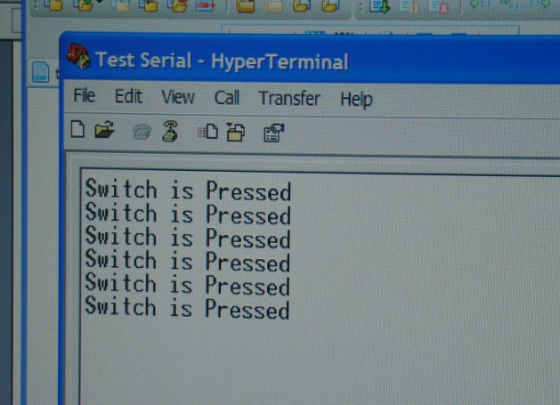
Experiment No. 3: Software UART test.
The objective of this experiment is to send a character string to PC using a software UART routine. The string will be transferred to PC and displayed on a Hyperterminal window when SW1 switch is pressed. The character string will be Switch is Pressed
Setup:Microcontroller side: Connect the uTx and SW1 pins to GP0 (pin 7) and GP1 ports respectively.
PC Side: Connect Rx (2), Tx (3), and Gnd (5) pins on the board to the corresponding RS232 port pins of the PC. Also, define a new connection hyperterminal window on a PC with the following settings.
BPS = 9600; Data bits = 8; Parity = None; Stop bits = 1; Flow Control = Hardware
Software
/*
  UART Test Experiment
  Rajendra Bhatt, Sep 4, 2010
  SW1 at GPIO1, uTx at GPIO0
*/
char Message[] = "Switch is Pressed";
char error;
int i;
void main() {
CMCON0 = 7;
TRISIO = 0x02;  // 0000 0010. GPIO 1 input; Rest are O/Ps
ANSEL = 0;
// Define GPIO.3 as UART Rx, and 0 as Tx
error = Soft_UART_Init(&GPIO,3, 0, 9600, 0 );
 do{
  // Detect logical one to zero
  if (Button(&GPIO, 1, 1, 0)) {
     Delay_ms(300);
     for (i=0; i< 17; i++) {
      Soft_UART_Write(Message[i]);
      Delay_ms(50);
     }
     Soft_UART_Write(10); // Line Feed
     Soft_UART_Write(13); // Carriage Return
  }


 }while(1);

}
Output: Everytime SW1 id pressed, you will see the character string Switch is Pressed displayed on the hyperterminal window.
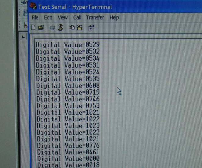
Experiment No. 4: Analog-to-digital conversion and software UART.
The objective of this experiment is read an analog voltage from a potentiometer, convert it to 10-bit digital number, and serially transfer it to a PC. The digital number will be displayed on a hyper terminal window.
Setup: Connect the output of potentiometer (POT2) to AN0 (pin 7). GP5 (pin 2) will serve as TX pin for Software UART so connect it touTx pin of TTL to RS232 Level Shifter circuit. Also connect Tx(3), Rx (2) and Gnd (5) pins on the board to corresponding pins of RS232 port of the PC.
Software
/*

  PIC12F683 Experiment Board
  Experimen No. 3 : Read analog voltage from AN0 and diplay
  on Hyperterminal window on PC using Software UART.
  Date: 06/25/2010
*/
char Message1[] = "Digital Value= ";
unsigned int adc_value, backup=0 ;
char *temp = "0000", error;
int i;
void main() {
CMCON0 = 7;
TRISIO = 11;  // GPIO 0, 1, 3 Inputs; Rest are O/Ps
ANSEL = 0;
GPIO = 0;
// Define GPIO.3 as UART Rx, and 5 as Tx
error = Soft_UART_Init(&GPIO,3, 5, 9600, 0 );
Delay_ms(100);

do {
 adc_value = ADC_Read(0);


 if(adc_value != backup) {

  if (adc_value/1000)
   temp[0] = adc_value/1000 + 48;
  else
  temp[0] = '0';

  temp[1] = (adc_value/100)%10 + 48;
  temp[2] = (adc_value/10)%10 + 48;
  temp[3] = adc_value%10 + 48;

 for (i=0; i<= 13; i++) {
      Soft_UART_Write(Message1[i]);
      Delay_ms(50);
     }

 for (i=0; i<= 3; i++) {
      Soft_UART_Write(temp[i]);
      Delay_ms(50);
     }
     Soft_UART_Write(10); // Line Feed
     Soft_UART_Write(13); // Carriage Return

 backup = adc_value;
 }

 delay_ms(100);
 } while(1);
}
Output
A digital number corresponding to the analog input will be displayed on the hyperterminal window. You can vary the potentiometer and the digital equivalent number will also change. Remember, the ADC is 10-bit so the number you see on the screen will be from 0000 to 1023.
More experiments will be posted on http://picboard.blogspot.com in future.
Please follow and like us:


")

")
Hi. Thanks for this. Where will I find the code for “Soft_UART_Write” and other routines?
Please download the zip file above and you will find the code in the word document.
Uart code is not giving right response with 12F675. Why?