Tiny DDS – Open source DDS generator
- Philippe Duboisset
- http://herptronix.blogspot.fr
- 66.287 Views
- advanced
- Tested
This project is an open source (hardware & software) DDS generator, based on: smart TFT module, AD9834, LM7171 fast amplifier.
Description
The homemade function generator is a quite common project on the internet. We can find different ways to do it:
- The quick & dirty way based on a DDS module bought on eBay
- The analog version based on a MAX038 / XR2206
- The clean way based on a FPGA and a fast DAC (e.g. http://www.circuitben.net/node/14)
- The software way (e.g. Arduino + R/2R DAC)
From my side, I wanted a small one which could fits my needs without being too expensive. According to me, such generator should at least:
- Be easy to use
- Output a signal from 1Vpp to 10Vpp (+/-5V), from 0 to 1MHz
- Have a low profile
- Without electric hazard (shall work on a 12V DC)
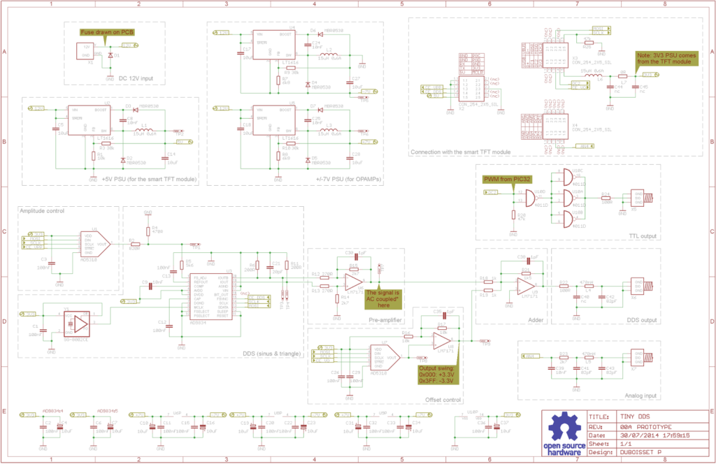
Schematic
Choosing the DDS chip
I first started to look for a cheap DDS chip on eBay; you have to be careful because most of DDS chips have only a sinusoidal output. Since I also want a triangular output, I have chosen the AD9834. According to its datasheet, this component is able to output a frequency of 37.5MHz from a clock of 75MHz But do not expect a clean waveform at such frequency: without an internal PLL, this signal would be defined by only 2 points.
From my personal experience, I consider that a waveform shall be defined by 10-20 points to be well restituted. Relying on a 75MHz clock, the maximal output frequency would be 7.5MHz This is not a very good performance for a professional equipment (even if the cheapest generators do not go above 4MHz), but it is quite reasonable for a hobbyist project.
The AD9834 can be found at $5 on eBay.
Amplitude control
The amplitude of the AD9834 can be controlled through different ways:
- Constant amplitude of 1Vpp (by default on most COTS), by wiring a resistor between the FS_ADJUST pin and the ground: this is quite annoying because an additional external amplifier will be need to set the amplitude to a desired level.
- Variable amplitude, by wiring a potentiometer between the FS_ADJUST pin and the ground: this solution is really easy to implement, but it will not allow a software management needed, for example, by the amplitude modulation.
- Software variable amplitude, by wiring a DAC to the FS_ADJUST pin. This solution is a bit more complex, but it will allow to implement some useful functionalities. I choose this way.
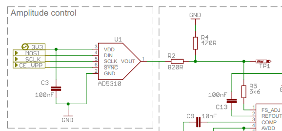
The amplitude will be set by the microcontroller of the smart TFT module (PIC32MX795). Unlike the other manufacturers (Atmel, ST ), Microchip did not include a DAC on their $10 chip An external DAC is needed (an AD5310 found on eBay for $0.8 10 bit / SPI, SOT23-6 package). A small voltage divider is put between the DAC and the FS_ADJUST pin in order to transform the 0-3.3V of the DAC into 0-1.2V handled by the AD9834:
Notice: the logical levels are reversed: the minimal amplitude is reached when the DAC output is 3V3 and the maximal amplitude is reached when the DAC output is 0V.
AC coupling
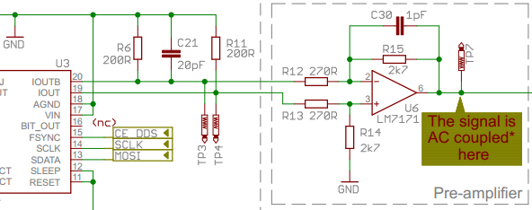
The AD9834 generates a signal with a non-null offset, variable according to the amplitude. At this point, this offset is very annoying and shall be removed. Two possible ways:
- A high pass filter (a simple RC filter): this solution ensures an ideal AC coupling, but is problematic for the low frequency signals (a huge RC filter would be needed for frequencies below 100Hz)
- A differential amplifier: it is possible with the AD9834 because this component already has a differential output (IOUT / IOUTB pins). This solution makes the AC coupling effective even for very low frequencies, even for a DC signal. Therefore, the AC coupling will not be ideal: a small offset will be injected, and possibly some additional distortions due to the tolerance of the components (OPAMP & resistors). Nevertheless, it remains the best way according to me.
The ratio R15/R12 is set such as the maximal voltage outputted by U6 is +/-3.3V.
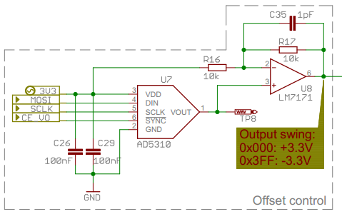
Offset control
Nothing difficult here: we just have to generate a DC signal between -3.3V and +3.3V. I use another AD5310 with a small OPAMP:
Notice: here again, the logical levels are reversed: the minimal offset is reached when the DAC output is +3.3V and the maximal offset is reached when the DAC output is 0V.
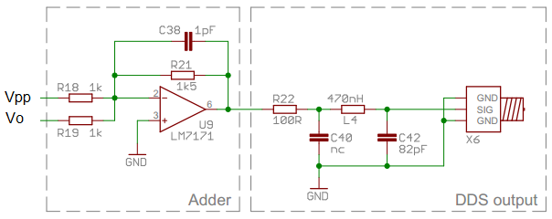
Final stage
Here, we have 2 signals: the one coming from the DDS (between -3.3V and +3.3V, AC coupled) and the one coming from the offset control (between -3.3V and +3.3V too). We just have to mix these 2 signals and amplify them to get a +/-5V output:
The LM7171 is able to output more than 100mA; nevertheless, the current is limited through a 100R resistor. A small LC filter is also implemented before the main output for filtering the 75MHz clock residual.
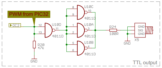
PWM output
Nothing complex here: a simple CMOS gate for buffering the PWM output of the microcontroller. I tried to use a fast comparator on the triangular output of the DDS, but the jitter was too important; I finally gave up this solution.
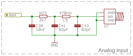
Analog input
Very minimalist A simple resistor for limiting the input current, and a common Pi filter. The sampling frequency is not very high (~ 1KHz) because the internal ADC of the microcontroller is also used by the touchscreen inside an ISR.
Power supply / regulators
The generator is powered by a standard 12V plug. Some switching regulators produce the 5V (for the smart TFT module) and the +/-7V (used by the analog stage). The 3.3V comes directly from the smart TFT. The LT1616 are an expensive components on Farnell, but I found these on eBay for $0.8. Notice that any buck regulator should do the job here (+5V@200mA, +/-7V@200mA).
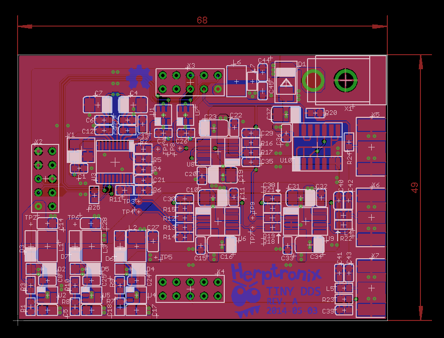
PCB
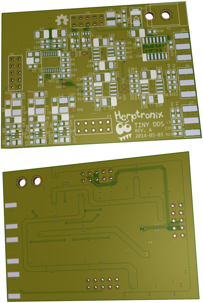
The whole schematic can be easily routed in a small PCB (smaller than a credit card). The PCB is composed of 2 layouts, with a common GND plan. The LM7171 shall be routed with care: due to its topology (fast OPAMP 400MHz), a bad layout will make it oscillate. For this reason, I also add a footprint for a small 1pF capacitor: if the layout is not correct, I should be able to limit the oscillations with it.
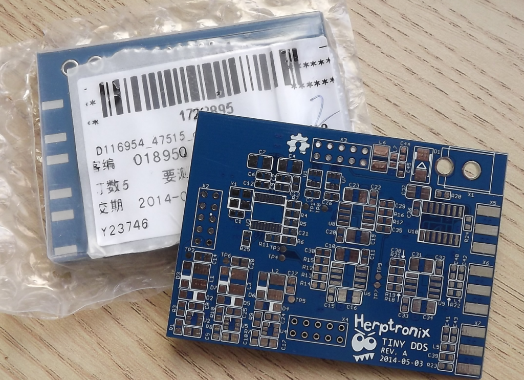
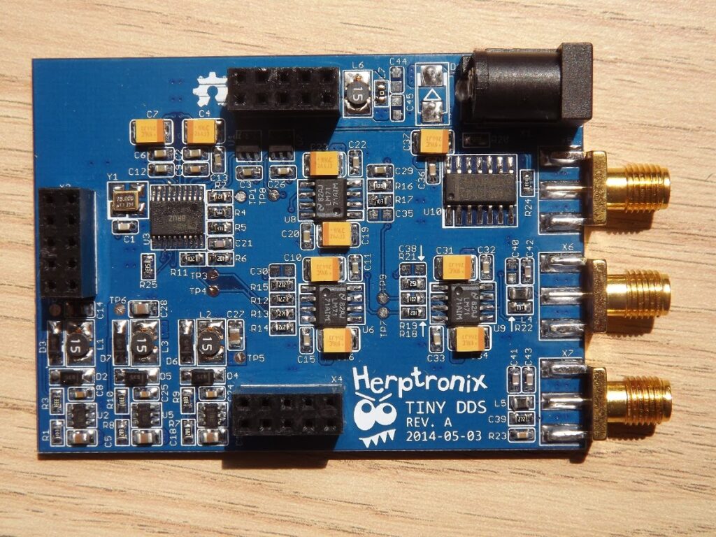
Assembling the board
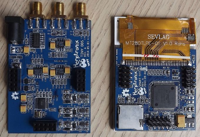
The PCBs (from SeeedFusion):
The finished board:
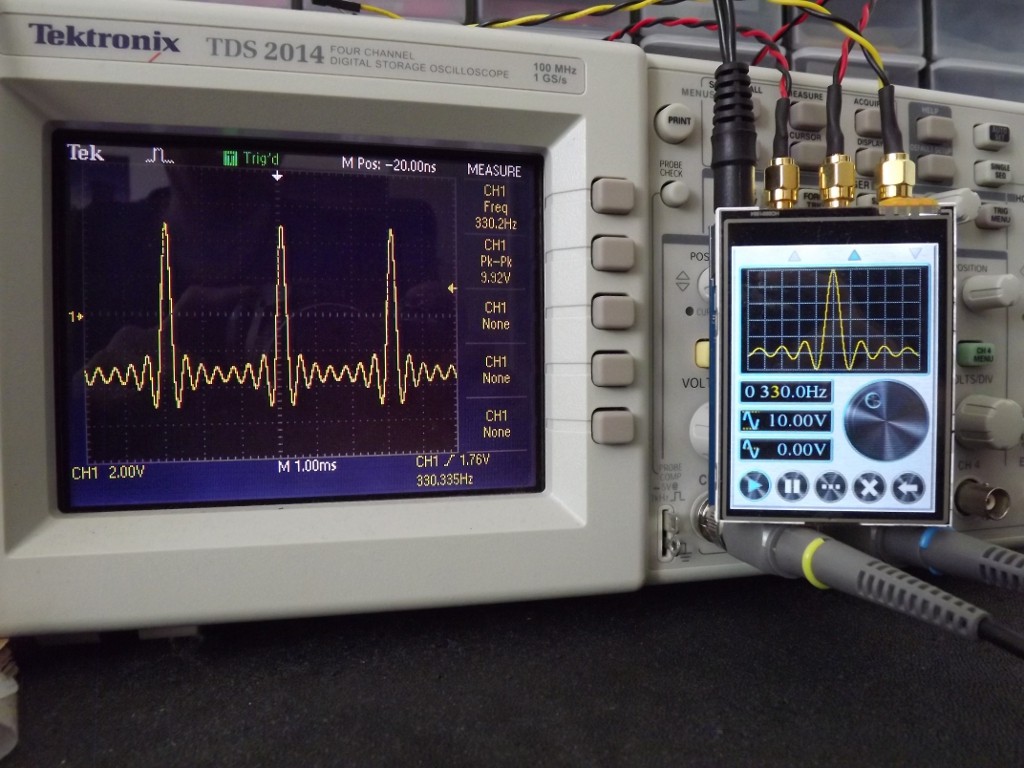
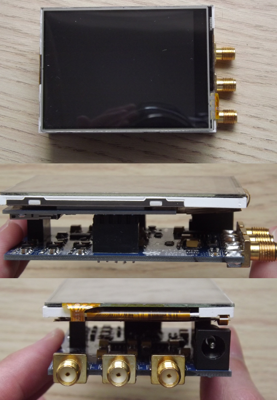
Assembled with the smart TFT:
Software
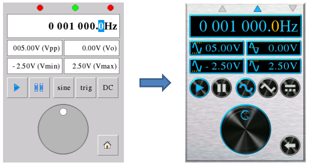
After a first quick & dirty attempt, I had to enhance the interface look; this one is working properly, but I admit that the old win95 look is really outdated. Moreover, there is a flickering issue on some widgets which are highly solicited (e.g. the frequency valueBox). The new interface is based on a brushed metal background, with dark widgets. I have also implemented the double buffering for the concerned widgets:
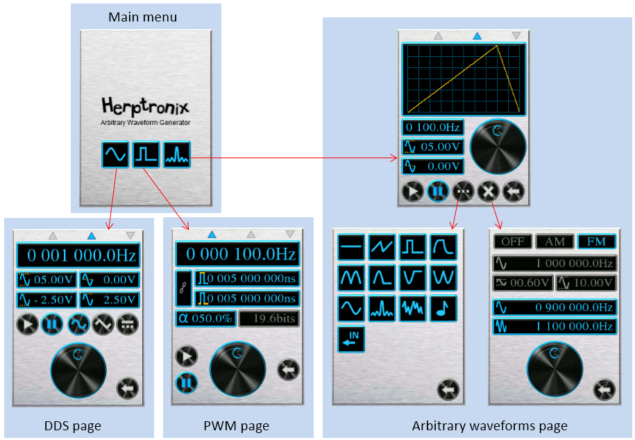
The new look is more modern (according to me; Im not a graphic artist :s). The interface is still very reactive, but the memory footprint literally explodes (more than 90% of the flash memory is used). The user interface is composed of 4 pages:
- DDS (sinus/triangle waveform, with frequency / amplitude / offset control)
- PWM (PWM signal only)
- ARB (arbitrary waveforms & modulations)
- A menu page
Sinus / triangle waveform generation
These waveforms are directly generated by the AD9834, just by configuring its internal registers through the SPI bus. Nevertheless, a small detail shall be handled by the program: the frequency register is coded on 28 bits, split on two 16 bits registers. The access to the frequency register is not an atomic operation and shall be buffered first (through the FREQ0 / FREQ1 registers).
Arbitrary waveforms generation
I use the internal DAC of the AD9834 to generate these signals: this solution allows to keep the whole analog stage as is (same amplitude / offset control). For using the internal DAC, I configure the AD9834 with a triangle signal of 0Hz; then, I set the phase register to obtain the desired output voltage.
Some basic waveforms are available, such as saw tooth, exponential, noise, sin(x)/x It is also possible to draw a waveform and play a wav file. However, there is a bandwidth issue: the AD9834 is accessed through a SPI bus, and even with a 20MHz clock, several microseconds are needed to send a single sample on the output. At the end, the microcontroller cannot provide more than 100kSPS (kilo Sample Per Second). Above this rate, the program is ran very slowly (most of the CPU time is spent into the ISR).
Go further
Even if this generator works properly, I have to admit that its electrical characteristics are closer to a gadget than a professional equipment (SNR below 45db). However, it would be easy to enhance its performances by modifying some components:
The DDS chip
A DDS such as the AD9102 is much more powerful than the AD9834; besides its more accurate DAC (14bits vs 10bits), its internal LUT can be reprogrammed: where the PIC32 can only provide 100kSPS, the AD9102 can provide up to 180MSPS (1800 time more). Unfortunately, this device is more expensive ($15/u at 100u) and is available only in LFCSP package (quite hard to solder).
The analog stage
The power supply should be changed first: the +/-7V coming from the buck regulators are obviously problematic (the output signal has some noise 1.5MHz @10mVpp). A simple power supply based on a toroidal transformer and some 78xx / 79xx would be better. The LM7171 OPAMPs should also be changed by a more appropriate chip (a current feedback OPAMP for example).
DAC
The 10 bits of the AD5310 might not be the wisest solution for this application: for 10Vpp, 1LSB is equivalent to ~10mV, which is pretty good if you use the whole range of the DAC! I reduced the range from 0-1023 to 0-920 due to the tolerance of the components, leading to an 11mV/LSB resolution. A 12 bits DAC would be a better solution here, thus a true voltage reference (the current one is derived from the 3.3V supply).




Great Article ! thank you for sharing.
I like how you presented it and the “go further” part.Il really want to take some time and try to do it by my own. It surely leans a lot about what is important to know for a good generator.
For graphic widget implémentation, did you use any graphical lib like eMWin ?
Finally how did cost the whole stuff ?
You said that the SNR is below 45 dB, how did you estimate it ?
In the first picture it seems you made a box, did you make a specific one or bought it on store ?
for the schematics and soft dev did you use proprietary software or GPL’d one ?