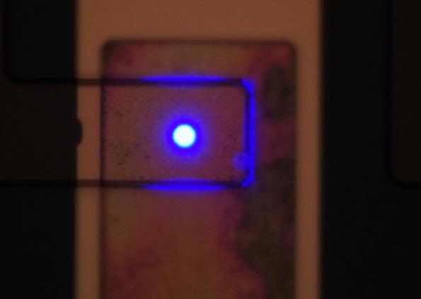
Taiwanese startup Mikro Mesa Technology has announced a major breakthrough in the mass transfer of microLEDs, with a non-compression low temperature bonding process allowing millions of microLEDs to be transferred in one step. by Julien Happich @ www.eenewsled.com
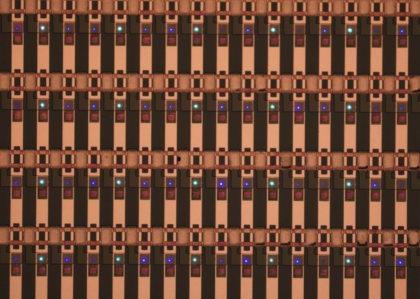
The company started cooperation with Chinese custom LCD display manufacturer Nanjing CLP Panda in 2017 and it took two years of development to deliver the first 3µm microLED chips. The ultra-small pixels means more microLEDs come out of the epitaxial wafers, and the mass transfer from wafers as large as 4-inch in diametre means up to millions of pixels can be transferred at a time, including multi-color microLEDs arrays. The large transfer area also reduces the number of necessary transfers for the production of large-size full-color displays, increasing yield.
According to Mikro Mesa insiders, the display technology can produce high-precision displays up to 1,800 dpi and could be applied to 55-inch or higher microLED TVs. The company anticipates the mass transfer process will make its microLEDs competitive with OLEDs for screens in wearables, smart phones, and AR headsets.
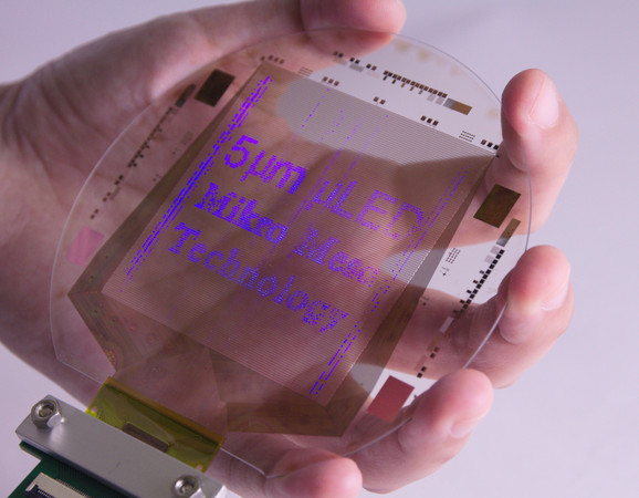
What’s more, due to its low process temperature, the technology is compatible with flexible and transparent substrates, enabling the design of transparent displays with much higher performance than today’s AMOLED displays.


