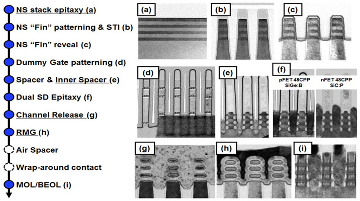
In less than two years since making a 7nm test node chip with 20 billion transistors, scientists have paved the way for 30 billion switches on a fingernail-sized chip. IBM with its Research Alliance partners, GlobalFoundries and Samsung, have unveiled their industry-first process that will enable production of 5nm chips.
The new 5nm technology is one of the first ICs based on GAAFET (Gate-All-Around) topology transistors and also probably the first serious application of EUV (Extreme UltraViolet) lithography.
Gate-all-around FETs are similar in concept to FinFETs except that the gate material surrounds the channel region on all sides. Depending on design, gate-all-around FETs can have two or four effective gates. Successfully, Gate-all-around FETs have been characterized both theoretically and experimentally. Also, they have been successfully etched onto InGaAs nanowires, which have a higher electron mobility than silicon.
IBM claims that it can fit in up to 30 Billion transistors on the chip using GAAFET on a 50 mm² chip. It’s a big move in the semiconductor world, as designs become increasingly complicated to apply. While comparing 5nm GAAFET to 10nm commercial chips, it will achieve a 40% performance boost and a 75% power consumption reduction, at similar performance levels. These are some big claims, so expect some big changes just around the corner.
“For business and society to meet the demands of cognitive and cloud computing in the coming years, advancement in semiconductor technology is essential,” said Arvind Krishna, senior vice president, Hybrid Cloud, and director, IBM Research. “That’s why IBM aggressively pursues new and different architectures and materials that push the limits of this industry, and brings them to market in technologies like mainframes and our cognitive systems.”
For more information you can visit the official announcement.


