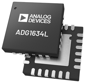
Analog Devices’ ADG1634L 4.7 Ω RON, quad SPDT switch has 1.2 V and 1.8 V JEDEC logic compliance
ADI’s ADG1634L is a monolithic industrial CMOS (iCMOS®) analog switch comprising four independently selectable single-pole, double-throw (SPDT) switches. Each switch has an input signal range that extends to the supplies and each switch conducts equally well in both directions when on. In the off condition, signal levels to the supplies are blocked.
All channels display break-before-make switching action, preventing brief shorting when switching channels. An EN input on the ADG1634L enables or disables the device. The switch is enabled with a Logic 1 EN input; the INx input defines the state of the SPDT switch (see Table 12 in the datasheet). When the EN input is disabled, all channels are switched off.
Where low distortion is critical for data acquisition and gain switching applications, the ultralow on resistance and on-resistance flatness of the switch is ideal. The device is well suited for portable and battery-powered instruments due to its iCMOS construction ensuring ultralow power dissipation.
An external VL supply provides flexibility for lower logic control. The ADG1634L is both 1.2 V and 1.8 V JEDEC standard compliant.
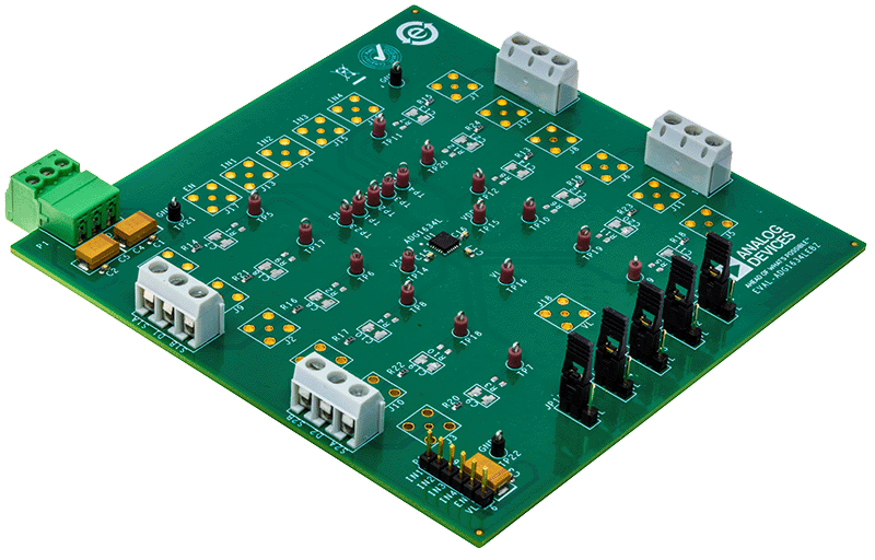
The EVAL-ADG1634LEBZ is the evaluation board for the ADG1634L.
Features
- 4.7 Ω typical on resistance for ±5 V dual supply at +25°C
- 1.2 Ω on-resistance flatness for ±5 V dual supply at +25°C
- 8.2 Ω maximum on resistance over temperature
- Fully specified at ±5 V, +12 V, +5 V, and +3.3 V
- ±3.3 V to ±8 V dual-supply operation
- 3.3 V to 16 V single-supply operation
- VL supply for low logic level compatibility
- 1.8 V JEDEC standard compliant
- 1.2 V JEDEC standard compliant
- Rail-to-rail operation
- 24-lead, 4 mm × 4 mm LFCSP
more information: https://www.analog.com/media/en/technical-documentation/data-sheets/adg1634l.pdf


