Class B Amplifiers
- Boris Poupet
- bpoupet@hotmail.fr
- 9 min
- 13.773 Views
- 0 Comments
Introduction
We have seen during the previous tutorial that Class A amplifiers are characterized by a conduction angle of 360° and a theoretical maximum efficiency of 50 %. In this new tutorial, we will present in detail another class of amplifiers known as Class B that have been developed as an answer to the low efficiency of the Class A.
In the first section, we will present what a Class B amplification consists of and an overview of its characteristics. We will see in a later section, however, that in order to work properly, two complementary transistors are needed in order to ensure the reproduction of the input signal, in what is commonly known as a push-pull configuration. Moreover, we will highlight an undesired distortion happening in Class B amplifiers and some possible solutions to limit it. At the last section of this tutorial, we will give a step by step method on how to calculate the theoretical maximum efficiency of Class B amplifiers.
Presentation of the class B amplification
The main difference with the Class A is that Class B amplifiers have a conduction angle of 180°. This implies that only half of the input signal is processed in order to realize the amplification process. To clarify this affirmation, the Figure 1 below compares the conduction angle of a Class A and a Class B amplifiers :
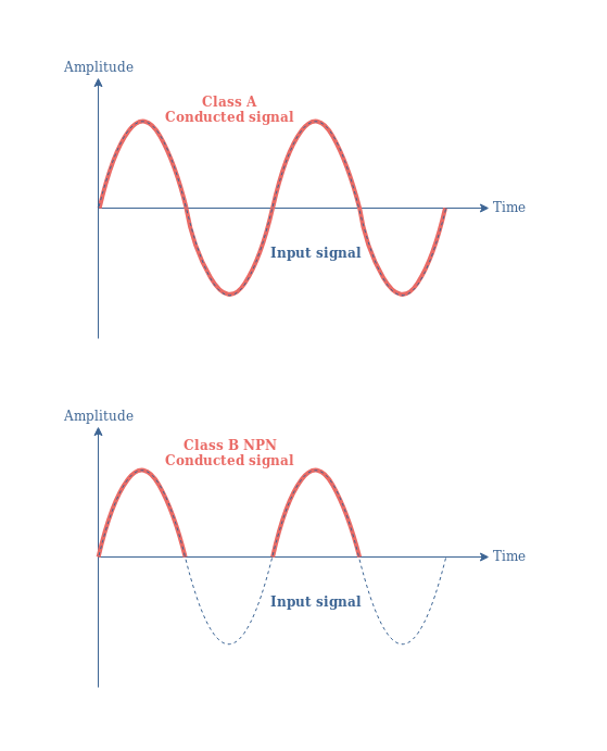
fig 1 : NPN-based class A and class B amplifier conduction angle
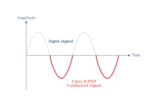
In Figure 1, we assume that the bipolar transistor (BJT) used is a NPN type. In a Class B amplifier, a PNP BJT would instead amplify only the negative parts of the signal such as shown in Figure 2 below :
To visualize better how a Class B configuration amplifies a signal, let’s consider two transistors of signal gain 5, one NPN and one PNP. The input signal of amplitude 1 and the output signals from the NPN and PNP transistors can be plotted in the same graph in Figure 3 :
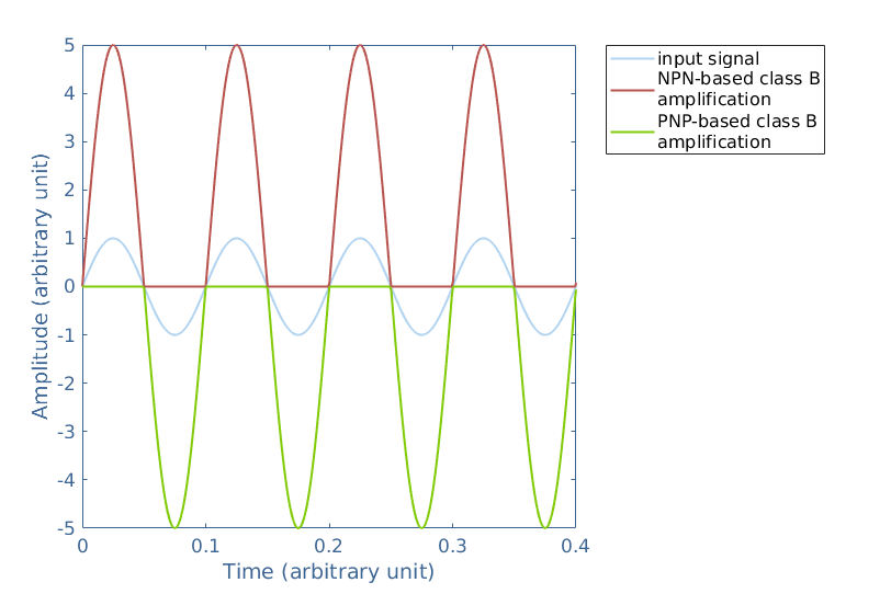
Since the NPN transistor only amplifies the positive half-wave and the PNP the negative half-wave, a faithful reproduction cannot be achieved with only one transistor. However, from Figure 3, we see that the superposition of both NPN and PNP output regenerates the shape of the input signal. In order to combine these two outputs, an NPN and a PNP transistor are placed in a so called push-pull configuration (Figure 4) that we will see in detail in the next section.
Another important characteristic of Class B amplifiers is the absence of DC bias on the base branch of the transistor. Therefore, Class B amplifiers can only conduct when the AC input signal is above the threshold level of the bipolar transistor +0.7 V. This fact plays an important role in triggering an undesired effect that is typical for Class B amplification, we will clarify this point as well in the next sections.
Push-pull configuration
The Figure 4 below presents the output stage of an emitter-follower push-pull configuration used for the Class B amplification in addition with the input signal, outputs of the NPN and PNP transistors, and final combined output :
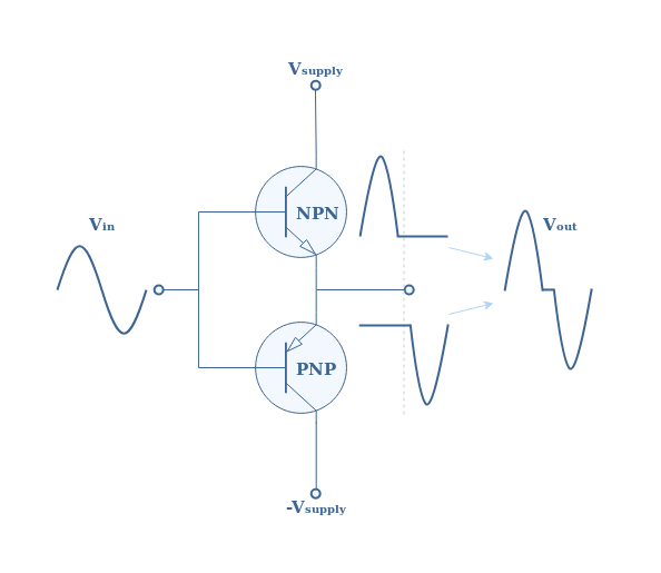
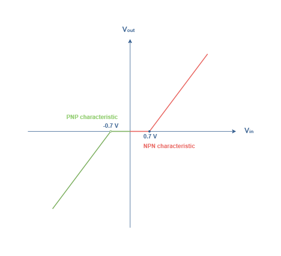
An undesired effect commonly known as crossover distortion is highlighted in Figure 4. There is indeed an interval around the zero amplitude crossover where the signal is not reproduced faithfully. To understand why this phenomenon happens specifically for class B amplifiers, we need to plot the (Vout, Vin) characteristic of the push-pull configuration :
From Figure 5, we can see that the Output/Input characteristic of a Class B push-pull configuration is only partially linear. Indeed, in a class B amplifier, the NPN and PNP transistors are working in the cutoff region, when the input signal is below the +0.7 V threshold (resp. above -0.7 V), the NPN transistor (resp. PNP) does not conduct the signal. This behavior creates an interval between -0.7 V and +0.7 V of 1.4 V where no signal can be conducted between the base and emitter branches. This explains the crossover distortion observed for Class B push-pull configurations.
Limiting the crossover distortion
The crossover distortion needs to be corrected especially for audio amplifiers where this effect is clearly perceptible. The first possible solution to limit or eliminate completely the distortion is to bias more or less the base branch depending on the desired linearity of the output signal. This solution will be detailed in the next tutorial since biasing slightly the base branch corresponds to a Class AB amplification.
Another solution is to modify Figure 4 by adding an operational amplifier in the circuit from the output to the input such as shown in Figure 6 below :
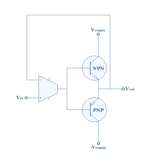
First of all, it is important to keep in mind that an operational amplifier compares two inputs on the inverting branch (-) and the non-inverting branch (+). Operational amplifiers have a very important gain and therefore a slight difference can be highly amplified. The output of an operational amplifier (in our case the common base branch) is equal to zero only if both input signals are strictly identical.
Let’s consider that a more or less important crossover distortion can be observed at the output of a class B negative feedback push-pull configuration. When the output signal is faithfully reproduced, which is out of the [-0.7 V,+0.7 V] interval, the potential at the branch +, V+ is strictly equal to the potential at the branch -, V–. Therefore, the potential difference V+-V– is zero and no signal is amplified by the operational amplifier. The common base branch of the bipolar transistor is thus not biased.
If the output signal is in the crossover distortion interval [-0.7 V,+0.7 V], a potential difference V+-V– will appear at the operational amplifier terminals and will be amplified into the common base branch which will bias temporary the transistors in order to correct the distortion.
To summarize, we can say this circuit “forces” the output to maintain the same shape as the input, therefore, reproducing a faithful signal.
Class B efficiency
As stated during the previous tutorials, the efficiency of an amplifier is defined by the ratio η=Pout/Pabs where Pout is the output power and Pabs is the power absorbed by the transistors and the load to realize the amplification process. In the following section, we can refer to the Figure 4, having in mind that the output signal is taken on a load resistance RL.
As already seen in the previous tutorial concerning Class A Amplifiers, we can decompose the output signals Vout(t) and Iout(t) such as :
With (V0,I0) representing the biasing and (vout(t),iout(t)) the AC component. The alternative signals can also be rewritten such as :
In AC regime, the dissipated power in the load PRL is expressed by the following ratio :
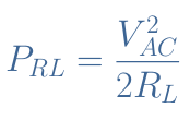
The instant power p(t) dissipated in both transistors can be written according to Equation 2 :

We can show through an integral calculus (that we will not detail here) that the average power PA dissipated in the transistors satisfies Equation 3 :

The total power Pabs delivered by the supply is therefore simply the sum of the power dissipated in both the load and the transistors PRL+PA :

Finally, the efficiency can be expressed by the ratio η=PRL/Pabs :
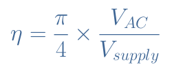
The efficiency is maximized when VAC=Vsupply, therefore giving a theoretical maximal efficiency ηmax=π/4=78.5 %. This is an important improvement of the efficiency when comparing back to the Class A amplification where only a theoretical maximum 50 % was achievable using a transformer, that in counterpart, leads to extra costs and complexity.
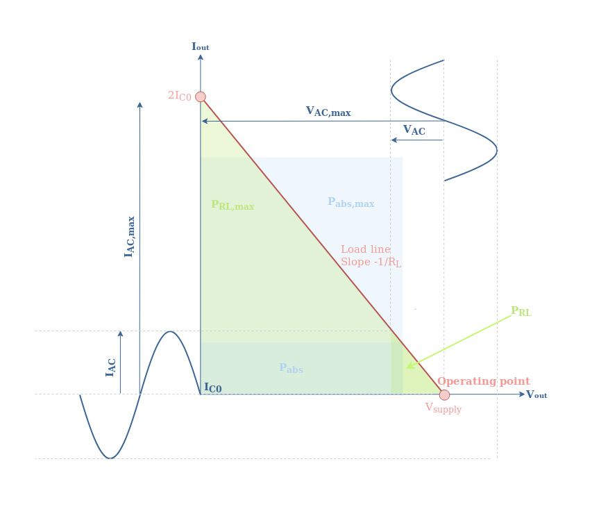
The above information can be summarized into a graph showing the distribution of power, presented in Figure 7. It is important to have in mind to plot this graph that VAC/RL=IAC . Moreover, to represent the quantity Pabs, we rewrite it such as Pabs=(Vsupply×√2/pi)×(IAC×√2/pi)≅((Vsupply×0.8)×(IAC×0.8).
Conclusion
This tutorial focuses on the Class B amplifiers by presenting the characteristics of such configuration. Indeed, we have seen that Class B amplification behaves as the opposite of Class A : it presents only a 180° conduction angle and does no reproduce the signal faithfully.
Later on, it is shown that it is possible to combine two transistors NPN and PNP in order to realize a push-pull configuration that reproduces the output signal more faithfully. The NPN transistor takes care of amplifying the positive half-wave and the PNP does the similar process for the negative half-wave.
However, a crossover distortion arises from this configuration that creates a misalignment of the positive and negative half-waves in the vicinity of the zero signal zone. This phenomenon, as detailed during the same section, comes from the zero biasing applied to the common base branch of the push-pull configuration, as well as from the threshold voltages of the NPN and PNP transistors, allowing only a conductivity of the signal out of the [-0.7 V,+0.7 V] zero signal interval.
After that we focus on the possible solution to implement in order to solve the crossover distortion. One of them is to bias the base branch according to the desired level of linearity we want to achieve. This solution will be detailed much more in the next tutorial concerning Class AB Amplifiers. The second solution is to add an operational amplifier to create a negative feedback loop in the circuit. The operational amplifier forces the output signal to follow the shape of the input signal, therefore limiting or eliminating the undesired crossover distortion.
Finally, we present a method to calculate the Class B efficiency. We conclude that the theoretical maximum efficiency is 78.5 %, which is much higher than class A configurations. This increase in efficiency is due to the low 180° conduction angle that allow the transistors to only absorb power from the supply when an AC input signal is indeed present.


