Common Collector Amplifier
- Boris Poupet
- bpoupet@hotmail.fr
- 15 min
- 15.096 Views
- 0 Comments
Presenting the Common Collector Amplifier
This article deals with another type of bipolar transistor architecture used to amplify signals that is commonly known as Common Collector Amplifier (CCA). The CCA can also sometimes be called emitter-follower amplifier and we will understand why later in this article.
The first figure below is a simplified electric diagram with no particular biasing circuit presenting the CCA configuration :
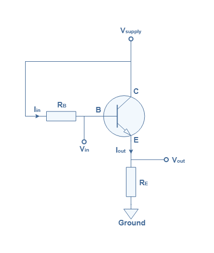
The main difference when comparing this architecture with the Common Emitter Amplifier (CEA) is that the output signals are taken on the emitter branch and the collector is always connected directly to the power supply, thus the name “Common Collector”.
It is shown further on that the voltage gain AV=Vout/Vin is approximately equal to 1. Moreover, the phase remains the same during the amplification process, the input and output signals are therefore very similar, hence the name “emitter-follower”. On the other hand, we will see that the current gain AC=Iout/Iin is high but has an upper limit.
Equivalent circuit
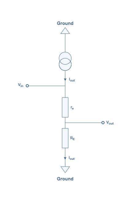
We can consider the bipolar transistor between the collector and emitter to be an ideal current source of amplification gain β where Iout=β.Iin. It also presents a small resistance given by re=25 mV/Iout known as “AC emitter resistance” or “small diode emitter resistance” and represents the dynamic resistance for small AC signals of the p/n junction of the bipolar transistor.
We see in Figure 2 an equivalent circuit of the CCA configuration of Figure 1 considering the transistor such as described above.
Voltage gain
It is easy to understand that in the configuration presented in Figure 1, the voltage gain is approximately equal to 1. Let’s indeed consider the voltage loop between the base and emitter. It comes automatically that Vin=RE.Iout=Vout and thus AV=1.
From Figure 2 we can clearly express the input voltage to be Vin=(RE+re).IE and the output voltage to be Vout=RE.IE. When expressing the voltage gain AV=Vout/Vin , the term IE disappears and we get the exact expression of the gain AV :

From this formula, it comes that AV<1 but usually RE>>re so the approximation AV=1 is justified. Since the voltage gain is always smaller than 1, Vout<Vin : the CCA cannot provide any amplification for the voltage signal.
Biasing method
To provide better stability, the base of the bipolar transistor is biased with a voltage divider network such as shown in the following figure.
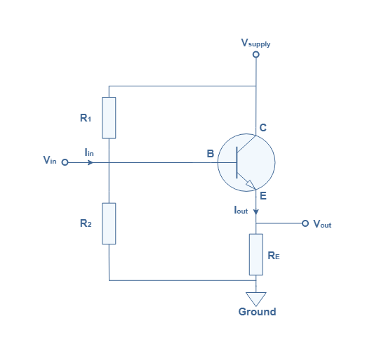
Since in a CCA configuration, Vin=Vout , the voltage divider network can be represented with a simpler equivalent circuit shown in Figure 4 :
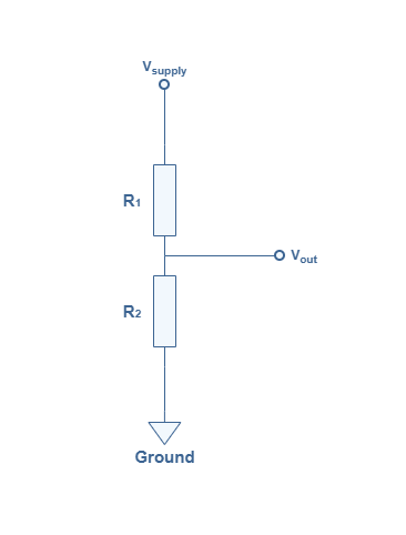
Using Kirchoff’s laws or Miller’s theorem in the circuit of Figure 4, it is easy to express the output voltage :
For a faithful amplification (no distortion or saturation), the output voltage should respect the condition Vsupply=2.Vout. Thus, the bias resistances R1 and R2 should approximately be equal. However, to be more accurate, the threshold voltage between the base and emitter VBE needs to be considered. For silicon-based bipolar transistors, the threshold voltage is a constant equal to VBE=0.7 V.
The full expression of the output voltage is hence given by Equation 2 :

Input resistance
The CCA amplifier is characterized by a high input resistance. The expression of the base resistance RB comes from Ohm’s law : RB=Vin/Iin. We have previously seen that Vin=(RE+re).Iout, thus :

With the condition that RE>>re the final expression of the base resistance can simply be written RB=β×RE. For this reason, the transistor’s current gain β is the most important factor to set the input resistance of a CCA configuration.
When considering a full CCA architecture with the biasing circuit, the total input resistance Rin satisfies the following formula :

The input resistance of a CCA is always very high which is useful to avoid loading down previous circuits connected to it.
Output resistance
If we consider the circuit of Figure 1, the output resistance is given by the emitter resistance RE which expression is RE=RB/β. However, the signal is always taken on a load resistance RL in parallel with the emitter branch and in this case the output resistance satisfies :

The output resistance on a CCA configuration is always very low and for this reason CCAs are used to drive low-resistance loads.
Current gain
Let’s consider a real CCA with a biasing circuit such as presented in Figure 3. The current gain AC is expressed by the ratio AC=Iout/Iin . The calculation of AI depends on the values of the bias resistances :
- If the parallel resistance R1//R2 is much greater than the base resistance RB, most of the current flows to the base and therefore Iin≅IB so that AC=β.
- If R1//R2 is lower or the same magnitude as RB, the current gain needs to be determined by the formula AC=Iout/Iin with Iin=Vin/Rin and Rin can be determined from Equation 4.
To sum up, if R1//R2>>β×RE , AC≅β. If not, AC=Iout/Iin. The transistor gain β is thus the maximum current gain achievable by a CCA configuration.
Example : Voltage, Current and Power gains of Common Collector Amplifier
Having in mind the expressions and characteristics of the voltage gain, the input and output resistances, let’s consider the following circuit with a transistor gain of β=200 and determine the voltage, current and power gains.
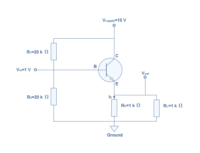
The output resistance is given by the emitter resistance RE in parallel with the load resistance RL :
The base resistance is given by RB=β.Rout=200×500=100 kΩ. The input resistance is thus given by the base resistance RB in parallel with the bias resistances R1 and R2 :
It can already be highlighted that Rin>>Rout such as mentioned previously. Let’s now calculate precisely the voltage gain AV. It is first considered that AV=1 so that Equation 2 is valid and therefore we can express the voltage drop across RE such as :

The current across the same resistance is thus given by IE=4.3 V/1 kΩ=4.3 mA. The small AC resistance can then be determined by re=25 mV/4.3 mA=5.8 Ω. Since RE=1 kΩ, we can confirm the hypothesis RE>>re.
Finally, the voltage gain is expressed by AV=500 Ω/505.8 Ω=0.989≅1.
In this example since R1//R2=10 kΩ<<RB=100 kΩ the approximation AC≅β is not valid and the current gain needs to be calculated with the formula AC=Iout/Iin.To compute the current gain AC, it is needed to determine the input and output currents Iin and Iout :
- The output current is simply Iout=Vout/Rout and since Vout≅Vin , Iout=1 V/500 Ω=2 mA.
- The input current is given by Iin=Vin/Rin=1 V/9.1 kΩ=110 μA.
Finally, the current gain is expressed by AC=2 mA/110 μA=18.2.
The power gain is given by AP=AV×AC=18. However, since RE=RL , the power given to the load is only half : AP,load=9.
The Darlington pair
We have seen that the transistor’s current gain β is the factor limiting the total input resistance and the output current Iout=β.Iin. Indeed, if β increases, the base resistance RB=β.RE increases and therefore Rin increases as well.
A simple way to overcome that limitation without having to purchase an expensive specific high gain transistor is through the Darlington Pair (DP) presented below in Figure 6 :
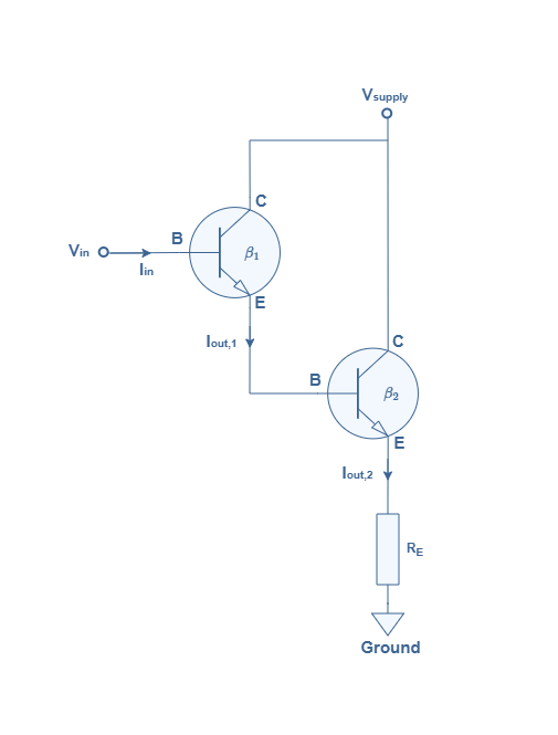
A DP consists in connecting together two bipolar transistor. The emitter of the first transistor is connected to the base of the second and both collectors are shorted to the power supply. We suppose the first transistor to have a gain β1 and the second is β2.
In this configuration, first of all, the input current is being amplified, the output of the first transistor is Iout,1=β1.Iin. This same current Iout,1 becomes afterwards the input current of the second amplifier which is a CCA configuration. The final output current is Iout,2=β2.Iout,1=β1.β2.Iin.
Finally, the total current gain of a DP is equal to Ω=β1.β2 which leads to a very high output current. Moreover, the base resistance can as well be expressed RB=Ω.RE which leads to a very high input impedance.
Conclusion
As a conclusion, we have seen that the Common Collector Amplifier does not amplify voltage signals since it’s voltage gain is strictly lower than 1 but usually can be approximated to 1, his nickname “emitter-follower” comes precisely from this behavior since the phase is also conserved. However, the current gain of a CCA is high with a upper limit equal to the transistor’s current gain β and depends on the values of the bias resistances. Moreover, we have seen that the input resistance is high and the output resistance is low. This characteristic makes the CCA configuration to be useful as a voltage buffer : the CCA can be interposed between a high and low impedance block to prevent any undesired loading. In the final section, we show an example of architecture called a Darlington pair that can overcome the limitation set by β for the input resistance and the output current.
In the next article, we present the last topology of the bipolar transistor : the Common Base Amplifier.


