Inverting OPAMP
- Boris Poupet
- bpoupet@hotmail.fr
- 11 min
- 3.261 Views
- 0 Comments
Introduction
The previous tutorial about the non-inverting operational amplifier has shown all the details of this op-amp configuration that takes the input signal on the non-inverting pin (+). This could be done by studying the ideal and real models and demonstrating all the important formulas. In this new tutorial, the same approach will be proposed for the inverting operational amplifier in which the input signal is supplied to the inverting pin (-) of the op-amp.
As a result, the ideal model will be detailed in the first section where the expressions of closed-loop gain, input, and output impedances are proven and discussed.
The second section deals with the real model for inverting op-amp, in which parasitic phenomena change the expressions of the important parameters mentioned above.
Examples of circuits based on an inverting op-amp are presented in the third section. This will highlight their role and possible uses in electronics.
Ideal inverting op-amp
In an inverting op-amp configuration, the negative (or inverting) input labeled with the sign “-” receives both the input signal Vin and the feedback loop. The positive (or non-inverting) input labeled with the sign “+” is simply connected to the ground.
An inverting op-amp configuration is presented in Figure 1 below, for which the symbol “∞” highlights that the circuit is ideal.
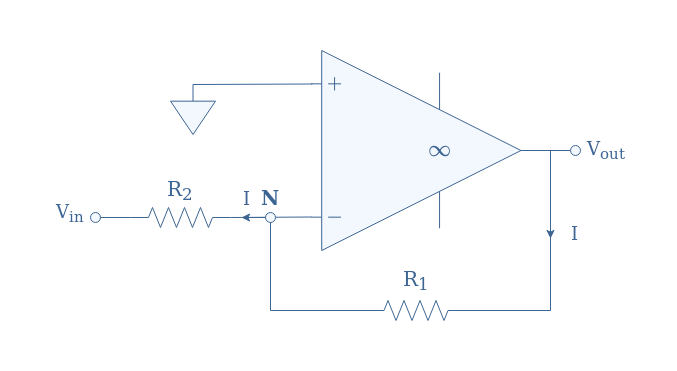
For the ideal configuration discussed in previous tutorials, it is assumed that no currents can enter either the non-inverting or inverting inputs, therefore, the feedback current I is found across R1and R2.
This is directly a consequence of the fact that we assume the node N to be a virtual earth and this results in particular to the equality V+=V–=Vin.
However, since the non-inverting input is connected to the ground, V+=0 , also implies V–=0. In order to get an expression for V–, we can use Millman’s theorem, which is a particular form of Kirchoff’s current law. The voltage signal at the inverting input can therefore be written according to the equation below:
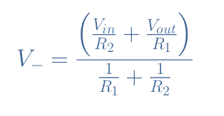
Since V+=V–=0, the above expression is also equal to zero. This can only be true if Vin/R2+Vout/R1=0, we can rearrange this expression to write the closed-loop gain (ACL) of an ideal inverting op-amp such as shown in Equation 1:
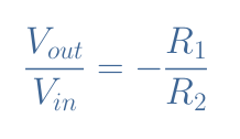
We can note that the closed-loop gain is strictly negative and can approach zero. This means that the output signal is inverted (the phase shift is 180°), thus the name “inverting op-amp”. Moreover, this configuration can amplify the signal if |ACL|>1 or reduce its magnitude if |ACL|<1.
Real inverting op-amp
The circuit diagram of a real inverting op-amp is presented in Figure 2:
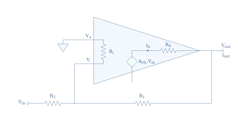
Such as we had done for the non-inverting configuration, we will now properly demonstrate the formulas for the closed-loop gain, input and output impedances for a real inverting op-amp.
Closed-loop gain
We begin the demonstration of the closed-loop gain by writing that Vout=AOL(V+-V–). Such as mentioned in the first section, the equality V+=0 is still valid because of the ground connection, this implicates that V–=-Vout/AOL.
In the non-inverting op-amp, V– could moreover be written as the result of a voltage division by the series configuration R1-R2. However, in the inverting op-amp, V– is rather expressed by a superposition of Vout and Vin:

In this formula, we can replace V– by -Vout/AOL, therefore we get:

We can finally express the ratio Vout/Vin in Equation 2, which is the definition of the closed-loop gain ACL:
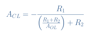
It is interesting to note that if the op-amp approaches its ideal model, AOL→+∞ and therefore Equation 2 can be simplified back to Equation 1.
Input Impedance
For an inverting configuration, the input impedance is simply expressed by Zin=R2, whether the op-amp is considered real or ideal. This observation is directly a consequence of the fact that the potential V– at the node N is equal to 0.
Output Impedance
In order to demonstrate the expression for the output impedance, we need to short the resistance R2 to the ground. First of all, we assume that no current enters the op-amp through the inverting and non-inverting inputs. Even if it is not exactly true, the several orders of magnitude difference justify this choice. This means that the current through R1 and R2 is the same and can be expressed by Vout/(R1+R2).
The current IRo across Ro can simply be expressed by performing a Kirchoff’s voltage analysis in the output loop simultaneously with the Ohm’s law formula:

Note that -Vin can be replaced by V– because the non-inverting input is directly connected to the ground.
The output current Iout is given by the sum IR1+IRo:

Since V– can simply be expressed by IR1×R1, we can inject this expression in the above formula. After factorizing by Vout every member in the right side of the expression of Iout, we can write the ratio Vout/Iout which defines the output impedance Zout of the configuration:

We can again emphasize that this expression is consistent with the ideal model, indeed when AOL→+∞ we get Zout=0.
Inverting op-amp example
Consider the following inverting configuration presented in Figure 3 for which we will compute the closed-loop gain, input, and output impedances:
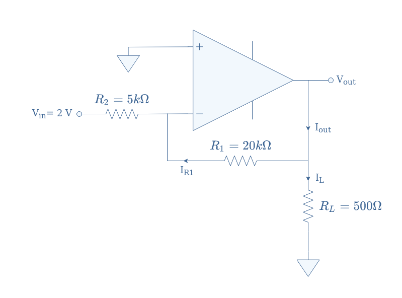
We need to remind that in most of the cases, the open-loop gain AOL is sufficiently high so that the ideal formula can directly be used for the calculation of the closed-loop gain ACL. This value is therefore given here by ACL=-R1/R2=-4.
Since Vin is given to be equal to +2 V, the output voltage is simply Vout=ACL×Vin=-8 V. If we still assume that no current enters through the inverting and non-inverting inputs of the op-amp, the current IR1 across R1 is equal to the current IR2 across R2. This last one is given by Ohm’s law: IR2=Vin/R2=0.4 mA.
The current IL across the output load is also given by Ohm’s law: IL=Vout/RL=-16 mA. By applying Kirchoff’s current law, we see that the output current Iout satisfies IR1=Iout+IL⇒Iout=16.4 mA.
Finally, we can say that the input impedance is given by Zin=R2=5 kΩ, the output impedance is given by Zout=Vout/Iout=490 Ω.
Conclusion
When the input signal is supplied to the pin “-”, the op-amp is said to be in an inverting configuration. The design and main properties of this configuration are presented in the first section that focuses on its ideal model.
In the second section, real inverting op-amp circuits are investigated, the demonstrations and exact formulas for the closed-loop gain and impedances are different and more complicated due to parasitic phenomena modelized by resistors.
However, in most cases, the real op-amps can be assimilated to their ideal model since the open-loop gain has always a value that is high enough to justify this choice.
An example of real configuration is shown in the last section, we present how to calculate the main characteristics of a configuration with the knowledge of the resistors value and input voltage.
Inverting and non-inverting configurations present very similar characteristics such as high input impedance and a low output impedance. The main difference comes from the closed-loop gain, which can only be strictly positive and higher than the unity for the non-inverting op-amp but strictly negative for the inverting op-amp.
The non-inverting op-amp will therefore always amplify the signal and keep it in phase, the inverting op-amp, on the other hand, inverts the phase and can either amplify or decrease the magnitude of the input voltage depending on the resistor values present in the feedback loop.


