MOSFET Amplifier
- Boris Poupet
- bpoupet@hotmail.fr
- 16.883 Views
- 2 Comments
Introduction to the MOSFET
We have already seen in detail that a signal amplifier can be made with a Bipolar Junction Transistor (BJT). There are however other types of transistors that can be used to build an amplifier architecture and in this tutorial, we will focus on one of them : the MOSFET (Metal Oxide Semiconductor Field Effect Transistor). In a BJT, the Base act as the command signal to control the current flow between the Emitter and the Collector. In a MOSFET the command branch is named the Gate and it controls the current flow between the Source and the Drain.
In the first figure below, the structure of a MOSFET is presented :
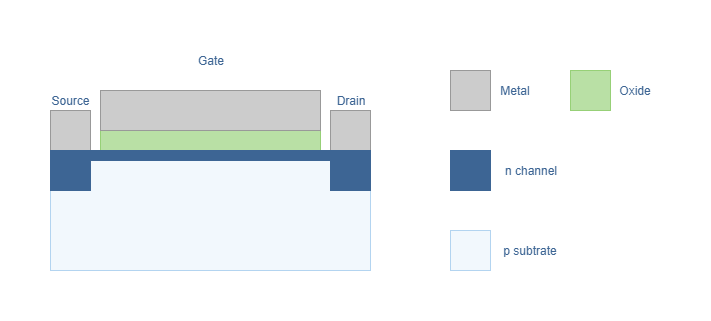
First of all, let’s define the meaning of “depletion” and NMOS terms. The term “depletion” here refers to the fact that a physical channel is linking the drain branch to the source branch. This means that a current can pass through the MOSFET with no voltage applied to the gate. The current can be blocked by applying a negative voltage to the gate, that by field effect, will push electrons and attract holes. The term “NMOS” refers to the fact that the channel is built based on a N-doped region of silicon (excess of electrons) on top of a P-doped substrate (excess of holes). The current traveling in the MOSFET is therefore positive. P-doped channel transistors on top of N-doped substrates are called PMOS and the current through this type of MOSFET is negative.
One interesting aspect of the MOSFET is the silicon oxide layer that provides a total insulation between the gate and the channel, hence, the current in the gate is considered to be zero. In reality, there is a small leakage current of a few pA (10-12 A). In Figure 2 we present the structure that will be considered for the rest of this tutorial :
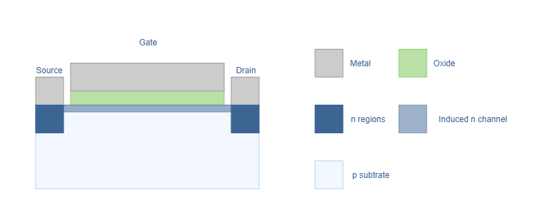
In this NMOS structure, there is no physical built-in n-channel between the drain and the source branches. This different structure is referred with the mention “enhanced”. The channel is electrically induced by applying a positive voltage to the gate that by field effect, attracts electrons and pushes the holes of the interface p-substrate/oxide.
Electric diagram
In Figure 3 below, we present a simple electrical diagram of a MOSFET. We define in this diagram the drain current ID, the drain voltage VD, the gate-source voltage VGS and the location of the gate, drain and source mentioned by the letters “G”, “D” and “S”.
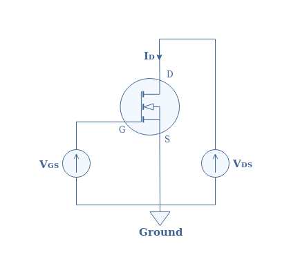
The gate and drain voltages VGS and VDS are mentioned with the subscript “S” because the source is grounded. Note that usually, the gate is a voltage source while the drain voltage is just measured and not imposed.
Electric behavior
Characteristic ID=f(VGS)
In this section, we will describe how the drain current behaves when :
- The drain voltage is imposed and the gate voltage varies : ID=f(VGS)
- The gate voltage is imposed and the drain voltage varies : ID=f(VDS)
Let’s first of all focus on the characteristic ID=f(VGS) as presented in Figure 4 :
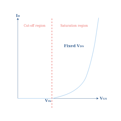
It is interesting to note that the creation of the conducting channel is not triggered instantly by a positive voltage since no drain current is observed when VGS<Vth where Vth stands for “threshold voltage”. This first region is called the “Cutoff” or “Subthreshold” region. In this mode, the MOSFET acts as an open switch, allowing no output current to be induced.
When the gate voltage is above the threshold value VGS>Vth, the drain current rises drastically. This second region is named “Saturation region” and we explain why further in the tutorial. In the saturation or “active” region, the current drain satisfies a parabola relation :

The factor k, known as conduction factor, depends only on physical parameters of the MOSFET : the ratio Width (W)/Length (L) of the conducting channel between the drain and the source, on the electron mobility μ and the value of the capacitance formed by the metal-oxide-semiconductor structure of the gate Cox :

It is interesting to analyze quickly this formula to understand the physics behind the MOSFET. The position on the numerator of μ, Cox and W indicates that if their value increases, the conduction factor and thus the current increases. Indeed, when W increases, the path for electrons gets wider and therefore the current increases. If the electron mobility increases, the electrons move faster, which in turns increases the drain current. If the capacitance increases, it will increase the drain current due to a higher concentration of electrons at the interface semiconductor/oxide. Finally, if the length of the conductive channel increases, the current will decrease since it faces a longer path, therefore a higher resistance.
An important parameter can be derived from Equation 1 and Equation 2 which is called the transconductance (gm) of the MOSFET and is expressed in Amps / Volts or Siemens (S). :

Equation 3 can be rearranged by expressing the difference (VGS-Vth) as a square root from Equation 1 and after a few steps we get :
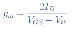
For a given MOSFET, that is to say, a fixed conduction gain, the transconductance only depends on the command voltage VGS and the current drain ID that are given by the characteristic ID=f(VGS) in Figure 4. The transconductance gives the gain of a MOSFET configuration but also the bandwidth, the noise performance and its linearity.
Characteristic ID=f(VDS)
To plot the second characteristic, we consider a set of gate voltages satisfying VGS,1<VGS,2<VGS,3<VGS,4. The characteristic ID=f(VDS) is constructed partially from the first characteristic ID=f(VGS). Indeed, the red dashed boundary in Figure 5 is given from the shape of the curve in Figure 4 :
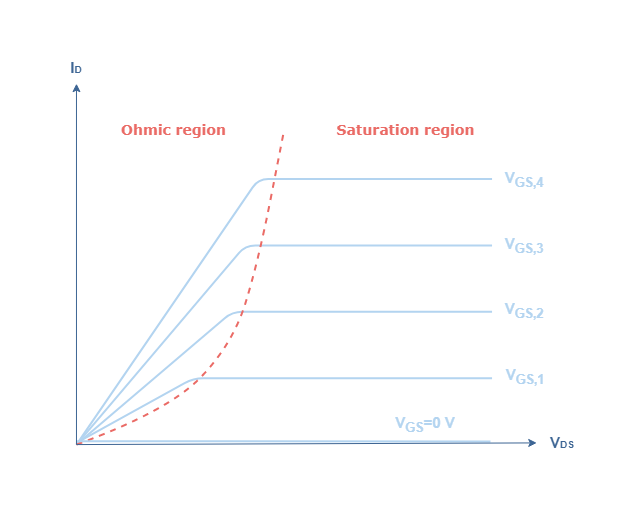
We can understand from Figure 5 why the saturation region first mentioned in Figure 4 is called such as. Indeed, in this region the drain current ID remains constant for a fixed bias voltage VGS no matter the value of the drain voltage VDS. This affirmation can be verified with the Equation 1 where VDS does not appear in the formula of ID. Therefore, the NMOS operates as a closed switch in the saturation region.
Before the saturation effect occurs, the MOSFET behaves differently in a region called “Ohmic”, “Triode” or “Linear” region. In this region, the expression of ID is quasi-linear affected by a decreasing parabola when VDS increases :

The boundary between the linear and saturation regions is given by the pinch-off voltage VP=VGS-Vth.
A MOSFET amplifier
A real and full MOSFET amplifier architecture is done by adding to the circuit of Figure 3 a biasing circuit, a drain, source and load resistor and coupling capacities :
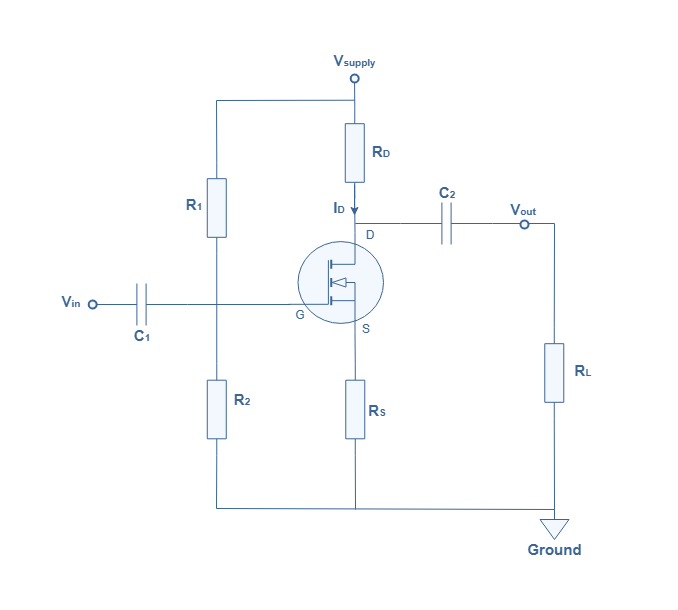
The biasing circuit consists of a voltage network divider, its role and functioning has been already dealt many times in the BJT amplifiers tutorial series, it is realized with two parallel resistor R1 and R2. The coupling capacitors C1 and C2 insulate the biasing DC voltage from the AC signal to be amplified. Finally, the output is delivered to a load, modeled by the resistance RL. The gate or bias voltage is given by :

The values of R1 and R2 are generally large in order to increase the input impedance of the amplifier and to decrease the ohmic power losses.
Input and output voltages
To simplify, we will consider that no load is placed in parallel with the drain branch. The input voltage is given by the gate to source voltage VGS and the voltage drop across the resistance RS given by RS×ID. Since by definition of the transconductance, ID=gm×VGS, the input voltage Vin can be factored by VGS such as :

The output voltage is simply given by the voltage drop across the drain resistance :

Voltage gain
The voltage gain AV is given from the ratio of Equation 7 and Equation 6, after simplifications it becomes :
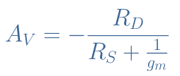
The sign “-” comes from the fact that in analogy with the BJT Common Emitter Amplifier, the MOSFET amplifier inverts the output signal : the phase is shifted of 180 ° or π rad.
Conclusion
This tutorial focused on Metal Oxide Semiconductor Field Effect Transistors (MOSFET) amplifiers. The MOSFET is an active component that consists of a conductive channel encapsulated between a semiconductor substrate and a metal/oxide structure. We have specially described enhanced NMOS structures that allow a current to pass when the command or gate voltage is positive and above a certain threshold value. We have seen that in order to understand the electric behavior of this transistor, two characteristics need to be analyzed. The first one, ID=f(VGS) gives the important parameter known as transconductance gm which helps to determine MOSFET’s amplifier gain that we give in the last section of the tutorial. It also gives the shape of the boundary between the linear and saturation regions of the transistor that can be represented in the second characteristic ID=f(VDS). From this analysis, three regions have been highlighted :
- The cutoff or sub-threshold region where VGS<Vth and no current drain circulates in the channel.
- The ohmic, linear or triode region where VGS>Vth and VDS<VGS-Vth and the drain current behaves linearly with the drain voltage.
- The saturation or active region where VGS>Vth and VDS>VGS-Vth and the drain current remains constant for a fixed gate voltage despite of drain voltage variations.
Finally, we have seen how a full MOSFET configuration can be achieved with a bias circuit and described the input and output voltages of the circuit and it’s voltage gain. The MOSFET amplifier inverts the voltage signal and provides a maximal absolute gain given by the ratio RD/RS.


You have not considered the load of amplifier while calculating gain.
What would it be if we take load resistance in effect while finding gain?
Hi Prince, do you refer to the output load Rl? In this case, you just replace Rd in equation 8 by Rd//Rl.