Operational Amplifier Building Blocks
- Boris Poupet
- bpoupet@hotmail.fr
- 11 min
- 3.178 Views
- 0 Comments
Introduction
In the introduction tutorial Operational Amplifier Basics, we have briefly seen that from the same op-amp, many configurations leading to different functions can be adopted, depending on how the feedback loop is designed.
In this new tutorial, we propose to detail the most common configurations along with their function.
We chose to group the configurations in three distinct major groups which will constitute the sections of this tutorial. The first section will, therefore, focus on the buffer designs,
The second section presents the amplifier configurations whose goal is to amplify a signal. Finally, the third section presents the operational op-amps which transform one or more signals to perform elementary mathematical operations.
Buffer configurations
A buffer amplifier is a block that is placed between two circuits which impedances are not matching: a high (resp. low) output impedance connected to a low (resp. high) input impedance. The goal of the buffer is to insulate the stages from each other and perform an impedance adaptation.
Since our tutorial concerns op-amps, we will only talk about voltage buffers but there are also current buffers.
Voltage follower
The voltage follower is a buffer that does not amplify nor inverts the signal. Consequently, its gain is equal to +1. The design of the voltage follower is very simple and simply consist of a short-circuit feedback to the inverting input (-) of the op-amp:
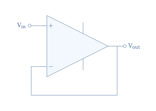
In order to really understand the purpose of this circuit, consider a Thevenin source VTh with an internal series resistance RTh that supplies an output load RL such as shown in Figure 2:
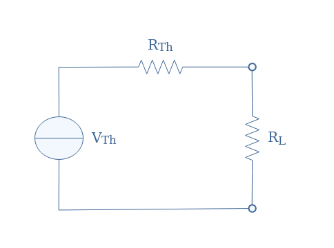
Due to the voltage division phenomenon, the source (VTh, RTh) will only be able able to provide a voltage VThRL/(RL+RTh) to the load. Let’s now place a voltage follower circuit between the source and the load:
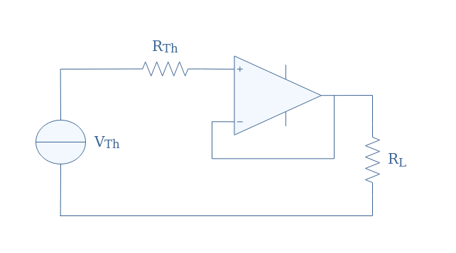
If we label Zin the input impedance of the op-amp, the voltage provided to the amplifier is Vin=VThZin/(Zin+RTh). However, since the input op-amp impedance is very high (Zin>>RTh), or even infinite if we consider the amplifier to be ideal, the input voltage in the op-amp can actually be simplified to Vin=VTh.
Since the voltage follower has a gain of +1, the output voltage is Vout=VTh. The voltage provided to the load can be written VThRL/(RL+Zout), however, the output impedance (Zout) of an op-amp is very low (Zout<<RL) or even equal to zero if we consider the op-amp to be ideal. As a consequence, the voltage provided to the load can be simplified to VTh.
In that example, we can see that the voltage VTh is entirely provided to the output load without any division phenomena thanks to the voltage follower. The circuit shown in Figure 3 actually acts as an ideal voltage source with zero Thevenin internal resistance.
Inverting buffer
If we consider the circuit in Figure 1, add resistors in the feedback loop and inverting input, and connect the non-inverting input to the ground, we obtain a circuit known as inverting buffer:
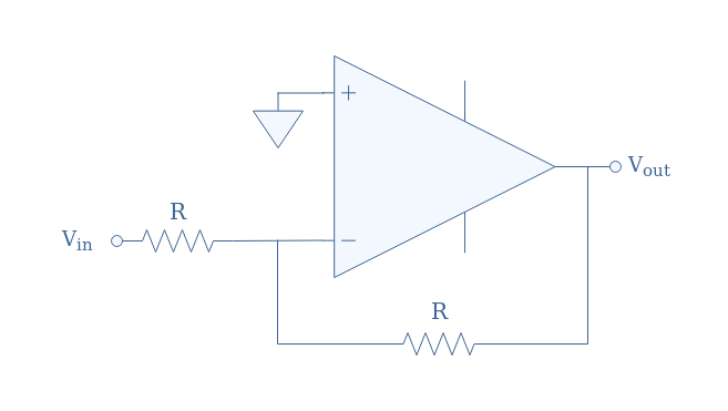
Assuming that the value of the resistors is strictly identical under the working condition of the op-amp, the gain of this circuit is -1. The signal is therefore not amplified but inverted: Vout=-Vin.
Amplifier configurations
In this section, we present some configurations for which the op-amp act as an amplification device, meaning that Vout>Vin.
Non-inverting amplifier
We consider a similar circuit to the one presented in Figure 4, the resistors are, however, not necessarily of similar value and the input signal is provided to the non-inverting input (+):
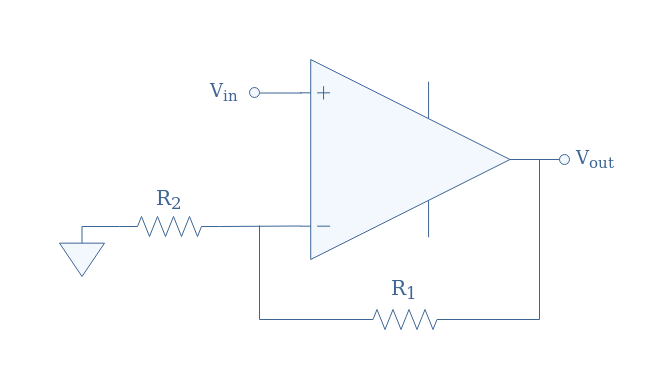
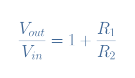
The gain Vout/Vin of the non-inverting amplifier is always strictly higher than +1 and given by Equation 1:
Inverting amplifier
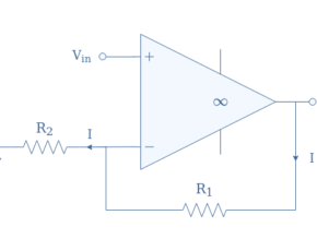
The inverting amplifier is designed by grounding the non-inverting input and applying the signal to the inverting input in the circuit presented in Figure 5.
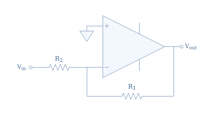
The gain is given here by the ratio -R1/R2, the negative sign assures that the signal is inverted.
Bridge amplifier
An inverting and non-inverting amplifier can be connected together to form a bridge amplifier. In this circuit, the input is common to both amplifiers while the output is taken on a load RL that is connected between the outputs of the amplifiers.
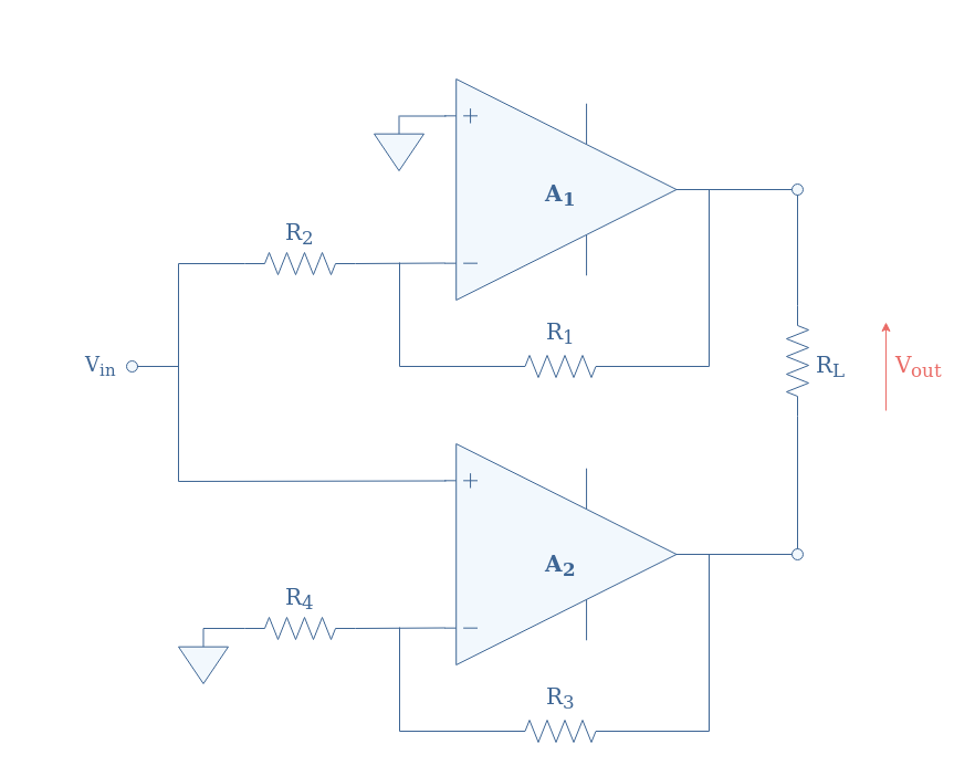
According to the previous subsections, the output of the first amplifier will be A1Vin with A1=-R1/R2. The output of the non-inverting amplifier is A2Vin with A2=1+(R3/R4).
Finally, with the direction convention chosen for Vout, the output of the bridge amplifier is given by (A1-A2)Vin. We can note that if the resistors are appropriately chosen, the magnitudes of the gain can be equalized (|A1|=|A2|), which allows the bridge amplifier to increase by a factor 2 the maximal amplification that a single amplifier could perform.
The advantage of the bridge amplifier is to be able to supply more power to an output load, by a factor 4. Moreover, a single-supply is able to drive both amplifiers that constitute the bridge amplifier, thus simplifying the design and cost of the circuit.
Operational configurations
Some op-amps configurations can perform elementary mathematical operations. In the following, we present the adder/subtractor and the derivator/integrator circuits.
Adder/subtractor
The adder configuration takes several voltages on its inverting input connected via resistors.
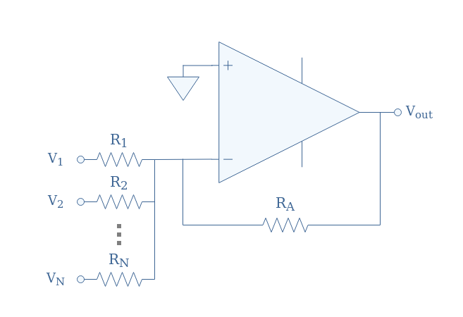
In the general case, the voltage Vout satisfies Equation 2:
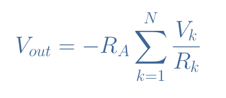
It is interesting to equalize all the resistances RA=R1=…=RN, which leads to a simplified formula where we can clearly see that the configuration presented in Figure 8 effectively adds the voltages:

Note that the presence of the minus sign means that the voltage sum is inverted. In order to add the voltages without an inversion, we can simply place an inverting buffer after this stage.
To realize a subtractor configuration, both the inverting and non-inverting output are used such as shown in Figure 9:
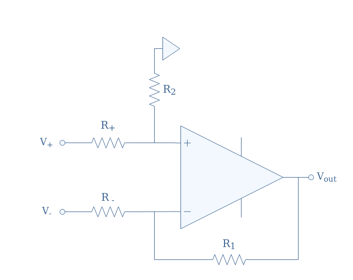
The configurations become again interesting when the resistor values are appropriately chosen so that R–=R1 and R+=R2. In that case, the subtractor function can be performed:

Derivator/Integrator
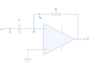
We start with the derivator which input is connected via a capacitor to the inverting branch, the feedback loop is connected with a resistor:

The output is proportional to the variations of the input signal given by the derivative function:
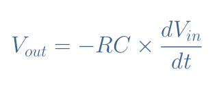
Derivators are useful to control the variations of certain physical parameters previously transformed in an electrical signal such as the temperature, pressure…
By inverting the position of the capacitor and resistor in Figure 10, we obtain the circuit of an integrator:
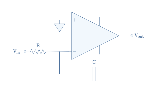
For this circuit, the output is proportional to the integral of the input:

Conclusion
We have presented in this tutorial some of the most important building blocks that can be realized with operational amplifiers. We chose to distinct these configurations in three groups depending on their function.
In the first section, we focused on the buffer configurations which do not amplify or modify the signal. The buffers can either be non-inverting (Vout=Vin) or inverting (Vout=-Vin) depending on which input the signal is applied. Thanks to their high input and low output impedances, buffers are mainly used to connect unmatching circuits together.
Amplifier configurations are presented in the second section with again, a distinction being made between inverting and non-inverting amplifiers. In both cases, it is the values of the resistors connected to the inverting branch that will dictate how much the output signal will be amplified. To conclude this section, we have presented the bridge amplifier which consists of interconnecting an inverting and non-inverting amplifier in order to increase the power that can be supplied to the output load.
Finally, operational configurations that can perform elementary mathematical operations are presented in the last section. An adder amplifier can be realized with an inverting op-amp with multiples inputs, a subtractor is realized with inputs on both inverting and non-inverting inputs. In both cases, it is interesting to equalize the resistors present in the circuit in order to realize additions and subtractions with any prefactor. Moreover, integrator and derivator designs are presented, they both have a capacitor in their design and are used either to integrate or derivate the input signal, these functions are widely used in automation.


