Texas Instruments’ power-path management solution features 20 mA termination and 1 A boost operation
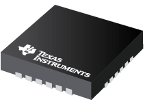
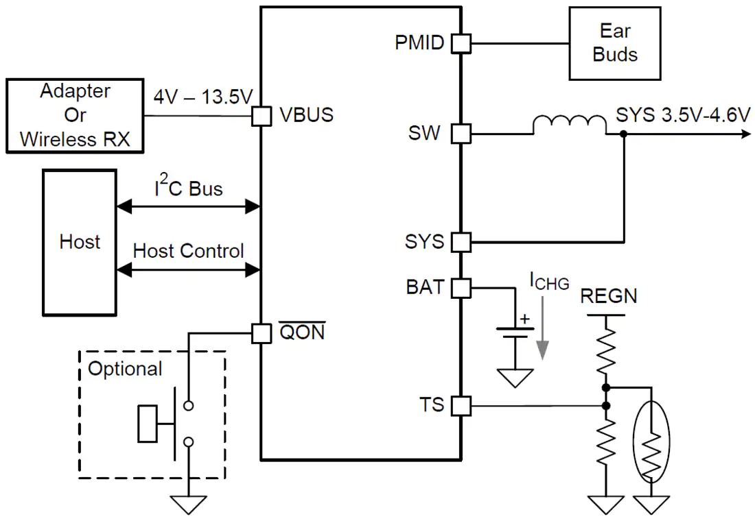
Texas Instruments’ BQ25619 integrates charge, a boost converter, and voltage protection in a single device. It offers ultra-low termination current for switching chargers to charge wearable devices by full-battery capacity. The BQ25619 low quiescent current reduces battery leakage to 6 µA in ship-mode, which conserves battery energy to double the device’s shelf life. The device is a highly integrated 1.5 A switch-mode battery charge management and system power-path management device for Li-Ion and Li-polymer batteries. It features fast charging with high input voltage support for a wide range of applications including wearables and earphone charging cases. The low impedance power-path optimizes switch-mode operation efficiency, reduces battery charging time, and extends battery run-time during the discharging phase. The input voltage and current regulation, low termination current, and battery remote sensing deliver maximum charging power to the battery. The solution is highly integrated with input reverse-blocking FET (RBFET, Q1), high-side switching FET (HSFET, Q2), low-side switching FET (LSFET, Q3), and battery FET (BATFET, Q4) between the system and battery. A bootstrap diode is integrated for the high-side gate drive to simplify the system design. The I2C serial interface with charging and system settings makes the device a truly flexible solution.
The BQ25619 supports a wide range of input sources, including a standard USB host port, USB charging port, USB-compliant high voltage adapter, and wireless power. The charger is compliant with USB 2.0 and USB 3.0 power specs with input current and voltage regulation. The device takes the result from a detection circuit in the system, such as a USB PHY device. The BQ25619 integrates a buck charger and boost regulator into one solution with a single inductor. The boost-mode supplies 5 V (adjustable 4.6 V / 4.75 V / 5 V / 5.15 V) on the PMID-pin and is used to save BOM and charge another battery by the control of PMID_GOOD. The PMID_GOOD pin is used to drive the external PMOS FET to disconnect boost output PMID from the attached accessories. The power-path management regulates the system slightly above battery voltage but does not drop below the 3.5 V minimum system voltage (programmable) with the adapter applied. With this feature, the system maintains operation when the battery is completely depleted or removed. When the input current limit or voltage limit is reached, the power path management automatically reduces the charge current. As the system load continues to increase, the battery starts to discharge the battery until the system power requirement is met. This supplement-mode prevents overloading the input source.
Features
- Single-chip solution to charge wearable accessories from an adapter or battery
- High-efficiency, 1.5 MHz, synchronous switch-mode buck charger
- Boost-mode with output of 4.6 V to 5.15 V
- Single input supports USB, high-voltage adapter, or wireless power
- Narrow VDC (NVDC) power-path management
- Flexible I2C configuration and autonomous charging for optimal system performance
- High integration includes MOSFETs, current-sensing, and loop compensation
- Low RDS(ON) 19.5 mΩ BATFET minimizes charging loss and extends battery run-time
- Low battery leakage current in ship-mode (7 µA), system standby (9.5 µA)
- High accuracy battery charging profile
Applications
- Consumer wearables, smartwatches
- Personal care and fitness
- Headsets/headphones
- Earbuds (true wireless or TWS) charging cases
- Hearing aids charging cases


