


Jan @ jasiek.me decided to use a flatbed scanner to trace out a footprint in KiCad. [via]
Some time ago I sourced a number of very cheap SD card sockets from China for a hobby project I was working on. Sadly, when it came to PCB design, I couldn’t find the footprints for this particular socket anywhere – the part being a proprietary invention of the factory rather than a cheap knockoff of a reputable brand like Amphenol or Molex for which drawings are readily available off of snapeda.com.
Creating footprints in KiCad using a scanner – [Link]
Please follow and like us:
RELATED POSTS
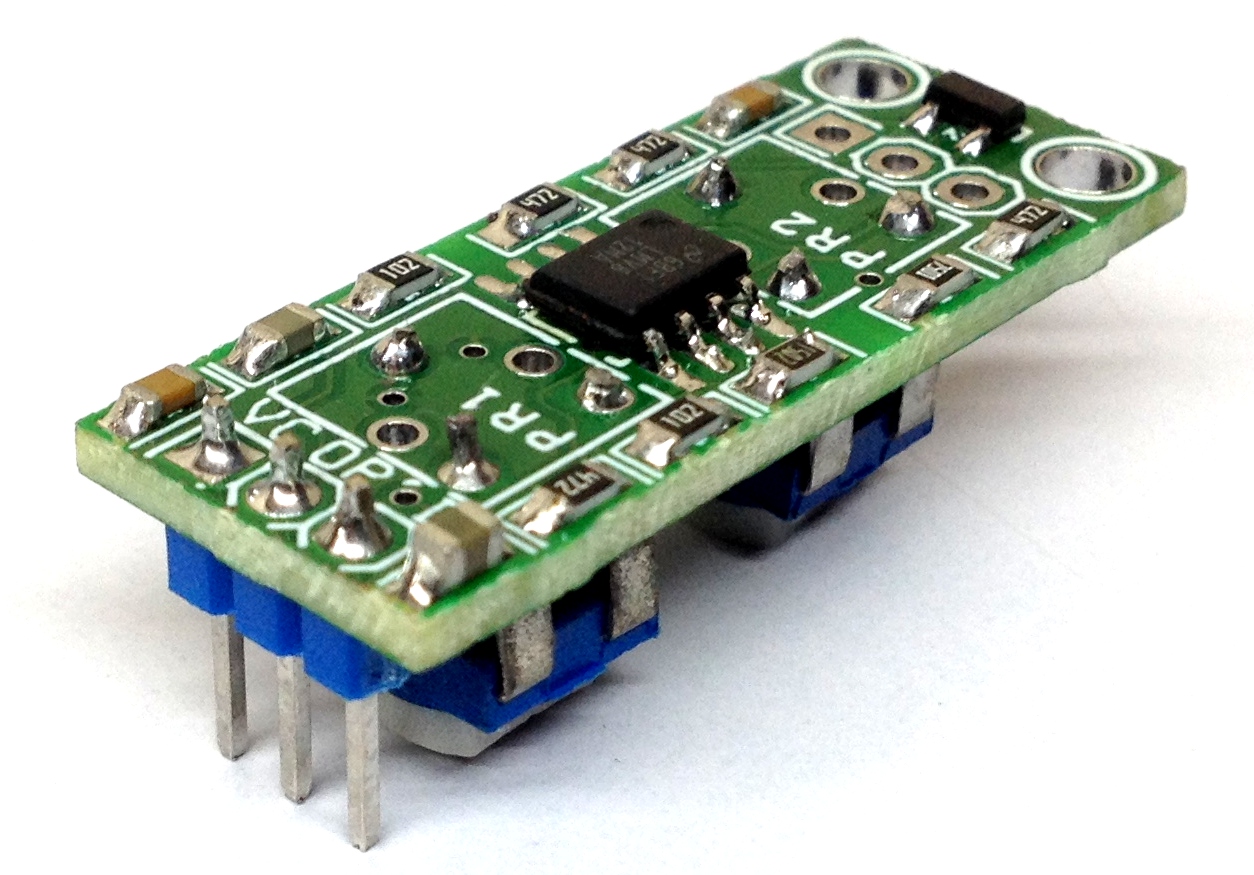 11 February, 2020 0 to 5V output Analog Hall Sensor for Foot Controller
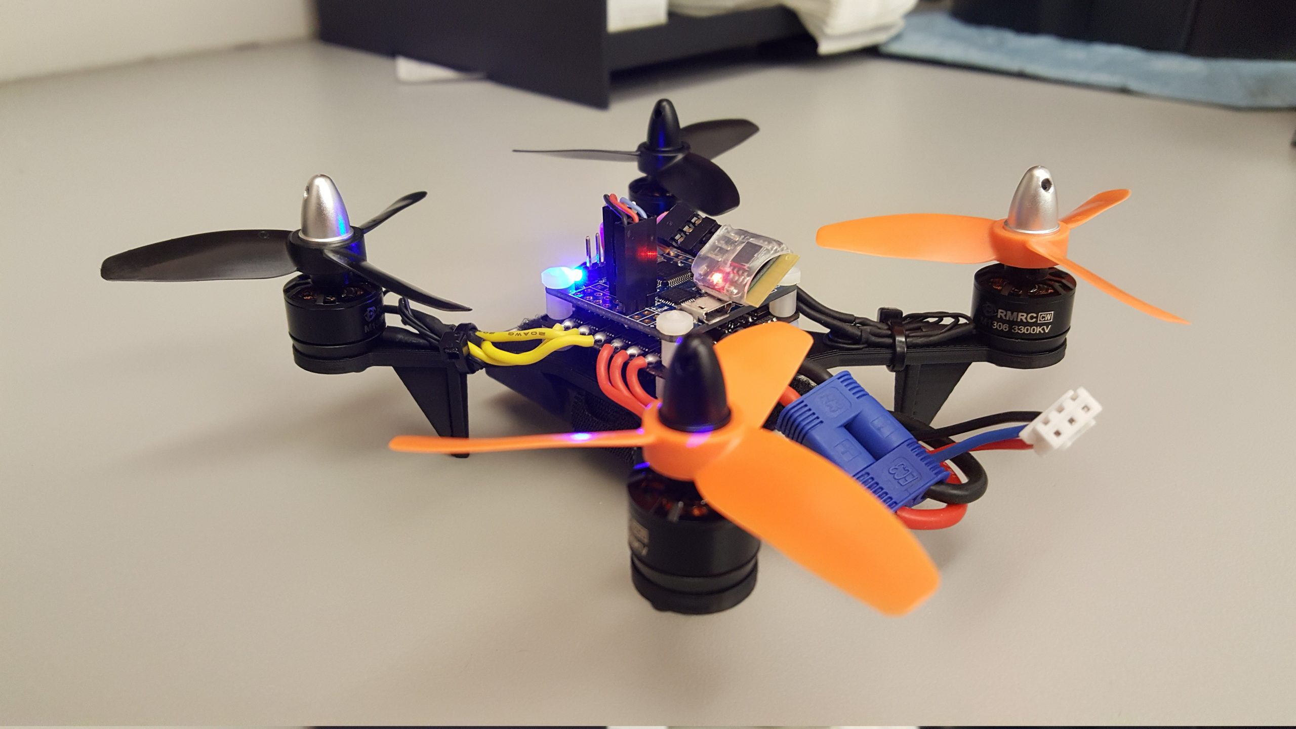 26 May, 2016 DIY Mini Quadcopter with 3D-Printed Frame and Custom Firmware
 10 January, 2018 XMOS VocalFusion- Background Noise Not a Problem Anymore
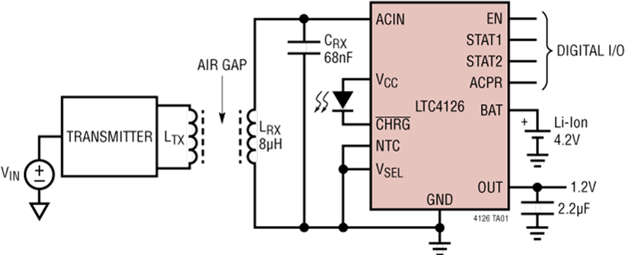 22 October, 2018 Εfficient Wireless Li-Ion Charger with Regulator Optimized for Low Power Wearables
 4 August, 2016 A New Record for Single-molecule Diode
 19 September, 2020 ADLINK Puts the Ease in Machine Vision AI Integration and Deployment

Subscribe
Login
0 Comments