


Author: Irena Zhuravchak, Technical Documentation Apps Engineer, Renesas Electronics, Lviv, Ukraine
Introduction
What do alarm systems, timers, smart keychains, and other notification systems have in common? They all need a buzzer, and consequently, a buzzer driver. The driver must satisfy specific criteria, such as delivering the requisite current and intensity, the possibility to add different patterns, and others.
The aforementioned audible systems are usually battery-operated, so there is a need to increase the voltage for reliable operation and great sound. This can be done with a voltage DC-DC boost converter. The boost converter driver provides the necessary voltage for system operation and also includes overcurrent and undervoltage protections.
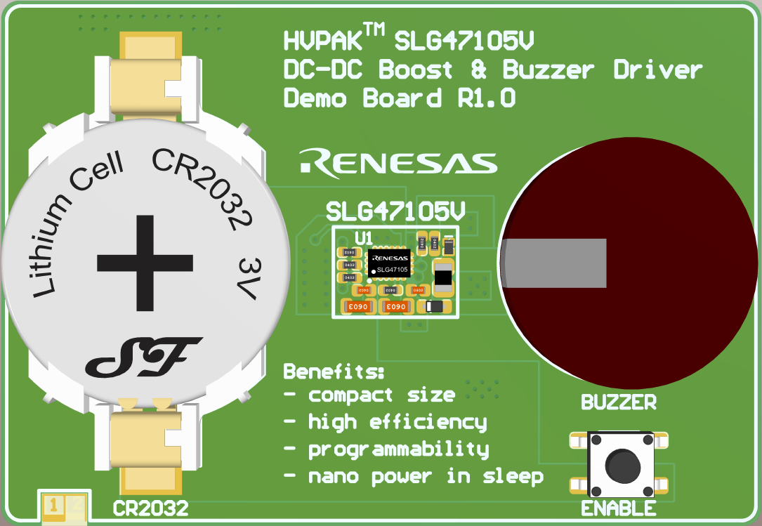
The HVPAK SLG47105 is a flexible configurable mixed-signal IC that combines a Boost DC-DC Converter and a Piezo Driver in a single package with a few external components.The main goal of this publication is to show how to configure HVPAK to drive a 2.5 kHz Piezo and how to create a Boost DC-DC Converter from 3 V to 13 V. The whole circuit is powered with a 3V CR2032 battery. Such a schematic can be used in devices that require short-term notifications (keychains for finding things, and others). When the push button is pressed, the DC-DC Converter boosts the voltage to 13 V which powers the Piezo Driver. Then the short pattern is played, and the circuit goes to sleep mode until the button is pressed again. When the circuit is ON – it consumes nearly 15 mA, and in sleep mode less than 50 nA. This ensures up to 800 activations on one battery.
Operating Principle and GreenPAK Design
The DC-DC Boost & Buzzer Driver Circuit Diagram is shown in Figure 1.
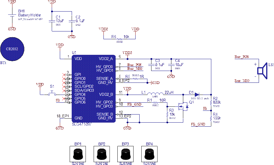
The design consists of a DC-DC Boost Converter and Buzzer Driver parts.
For the DC-DC Boost Converter, the PWM0 forms the ~197 kHz signal. The DFF1, DFF5, and DFF6 form the clock for a soft start to reduce inrush current, which can occur when the device is first turned on. Minimum and maximum duty cycles are set by Pipe Delay and CNT4/DLY4.
The VDD and VDD2_B are connected to a 3 V battery. VDD2_A is connected to Boost output. To monitor this voltage, the resistors R2 and R4 form the resistive divider with a feedback signal, which goes to PIN20 (Analog Input). This feedback voltage is compared with 1024 mV Vref by ACMP1H forming the ACMP signal which goes to the CHOP input of the PWM Chopper 0. If the VDD2 exceeds 9.5 V, the ACMP signal is HIGH and chop the formed PWM signal. The PWM Chopper 0 output goes to HV OUT CTRL1 (Half Bridge) input IN0. Then PIN 9 drives an NFET of Boost Converter.
To reduce the current consumption, a resistive divider is connected to PIN 10 (Low Side ON) with a GND input.
Note: it’s possible to change the ACMP1H Vref and boost the voltage up to 13 V.
The GreenPAK Design is shown in Figure 2.
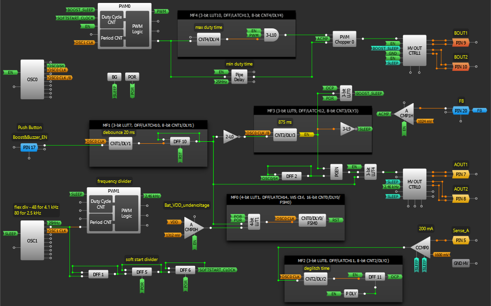
The HV OUT CTRL0 (Full Bridge) drives a Piezo. PWM1 is used as a frequency divider and forms a 2.5 kHz signal (resonant frequency of a piezo), this signal comes to PH input of HV OUT CTRL0.
The 3-bit LUT4 forms the EN signal for the HV OUT CTRL0. It consists of the sound pattern signal and the general EN signal. The PGEN generates the sound pattern (01010101101011). The EN signal – the general ENABLE signal for the whole design is HIGH for 875 ms (CNT3/DLY3 One Shot) if the button is pressed (MF1) and the VDD is higher than ~2.6 V (ACMP0H + MF0).
The 3-bit LUT9 inverts the EN signal forming the SLEEP signal to shut down the blocks when they are not used to reduce the power consumption.
The 3-bit LUT0 forms the BOOST_SLEEP signal. The Boost will power down if there is no POR signal, the SLEEP signal is HIGH, or the OCP signal is HIGH. The CCMP0 monitors the piezo current and if it exceeds 200 mA, the OCP signal is HIGH (MF2).
Design Testing
Channel 1 (blue / 1st line) – PIN 7 (Piezo).
Channel 2 (yellow / 2nd line) – GND (current).
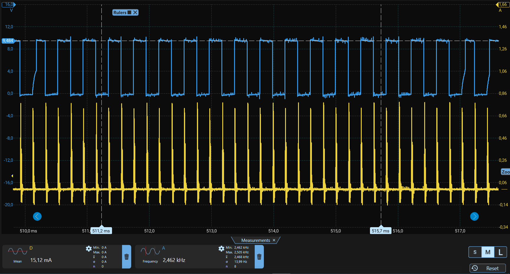
As can be seen in Figure 3, the VDD2 level is 9.5 V as expected, and the Piezo frequency is 2.5 kHz. The average current consumption is 15 mA. The current in sleep mode is below 50 nA, which means up to 800 activations without replacing the battery!
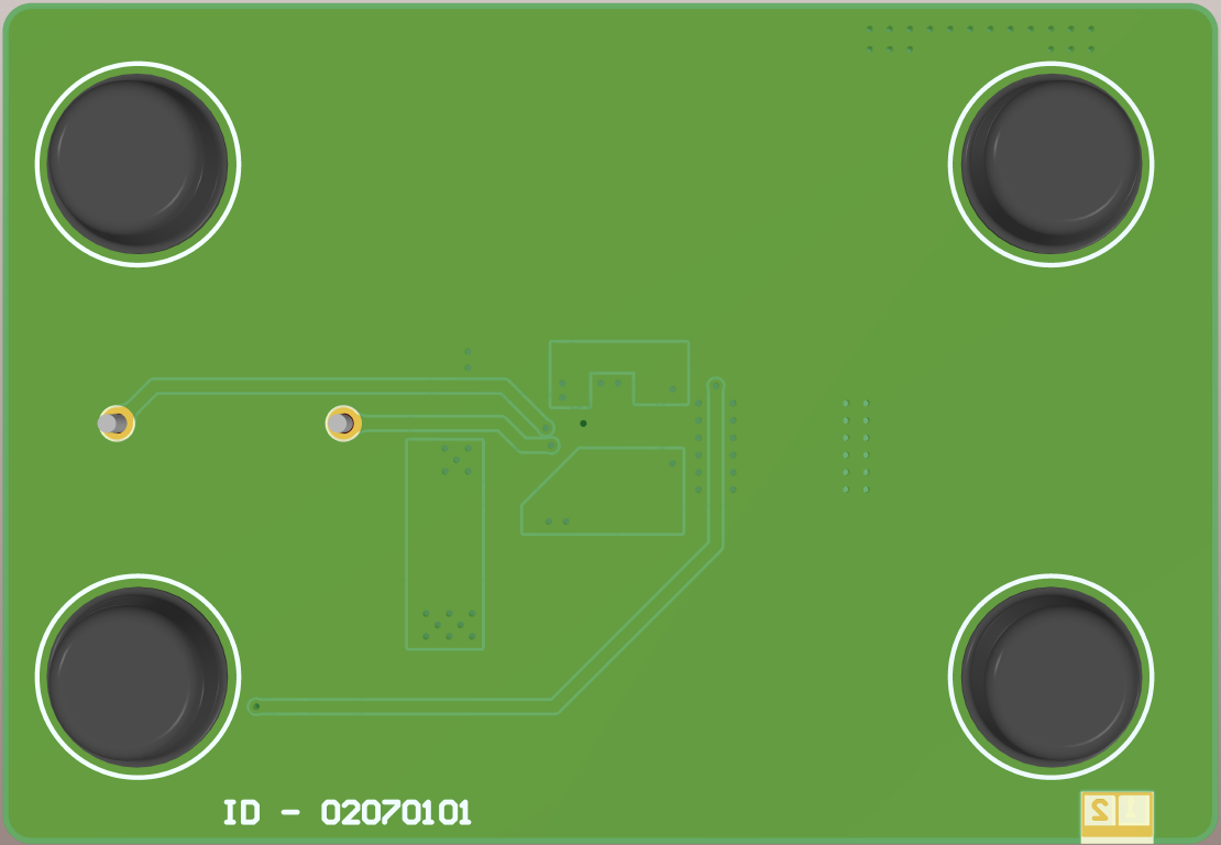
PCB Design
The proposed Demo PCB Design is shown in Figure 4 (top) and Figure 5 (bottom). As can be seen in Figure 4, the design is so compact that it can be placed under the buzzer.
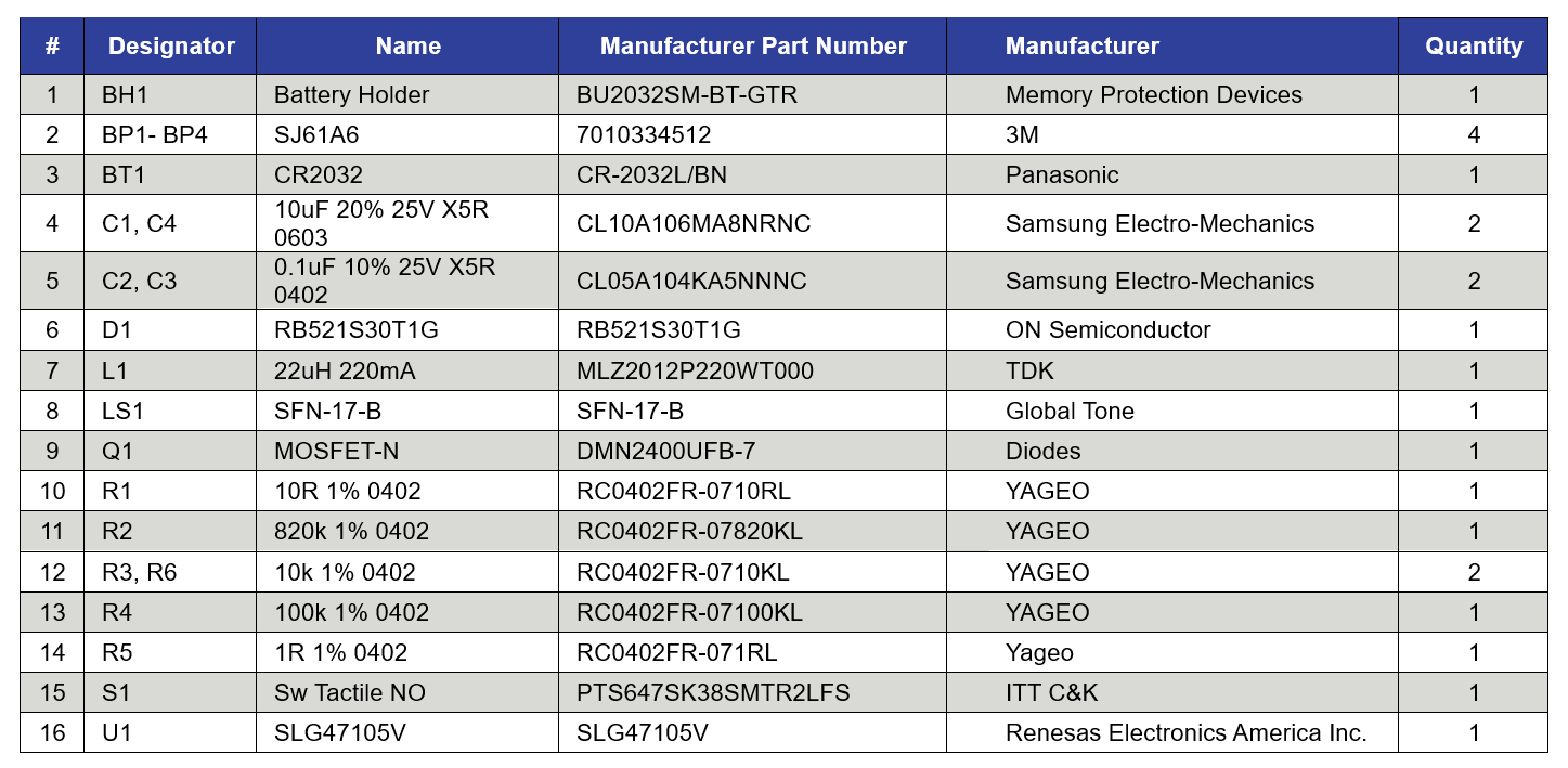
List of Materials Used to Manufacture a Boost & Buzzer Driver
Conclusion
This article outlines the configuration process for the HVPAK SLG47105 to establish a Boost & Buzzer Driver device compatible with a single 3V CR2032 battery. By its notably low current consumption, it can accommodate up to 800 activations without necessitating battery replacement.
The internal resources of the device offer considerable flexibility, facilitating seamless adaptation to the specific requirements of users.
RELATED POSTS
 31 March, 2017 Electrons Counter-Intuitive Movement
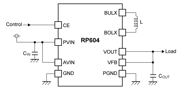 10 January, 2018 @Ricoh RP604 300 mA Buck-Boost #DCDC Converter for #IoT applications
 21 April, 2022 STMicroelectronics LD56020 Ultra-Low Noise LDOs
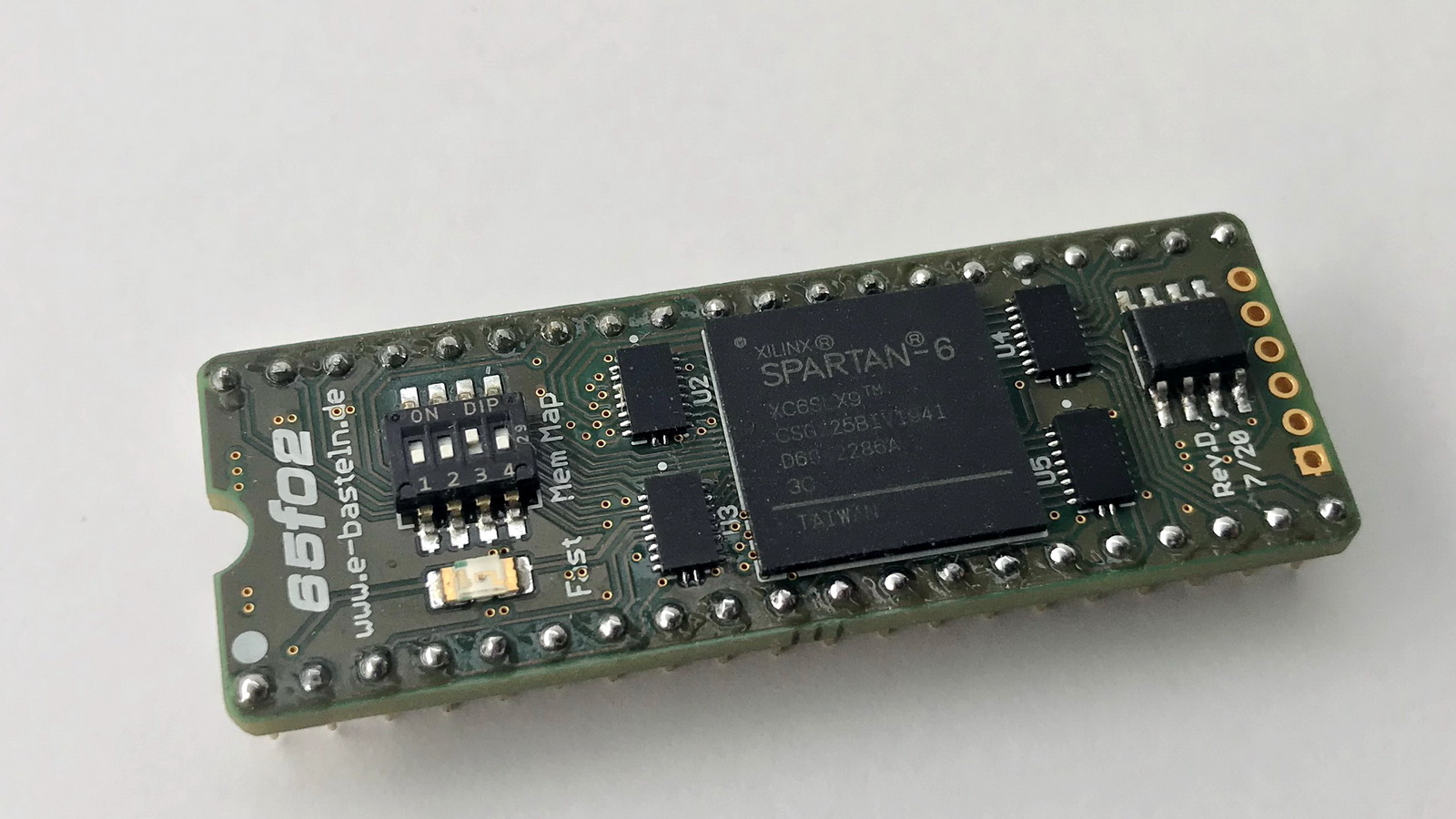 20 January, 2023 Implementing the 100 MHz 6502 In an FPGA
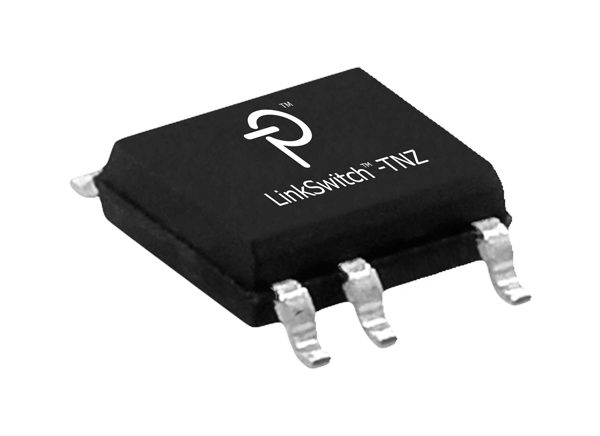 23 July, 2021 Power Integrations LinkSwitch-TNZ Off-line Switcher ICs
 23 November, 2018 Commercialised 1005-size metal power inductor