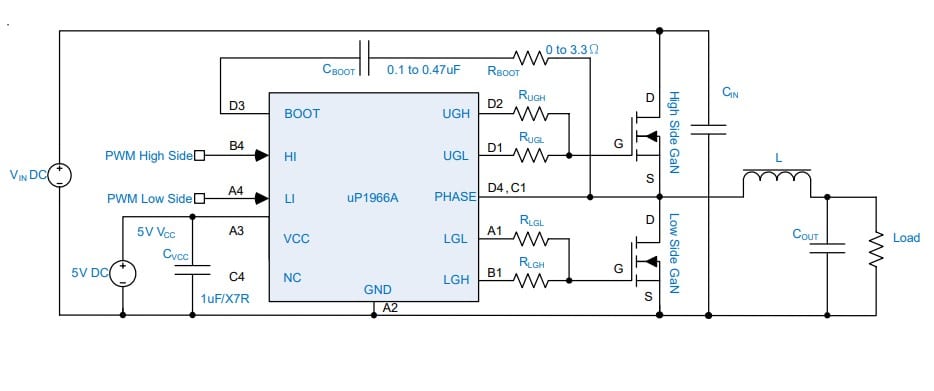
The uP1966A from uPI Semiconductor is designed to drive both high-side and low-side GaN FETs in half-bridge topologies. It integrates an internal bootstrap supply and UVLO. The uP1966A has split gate outputs that can operate to several MHz on both high and low side drive channels, providing the ability to adjust both turn-on and turn-off transition times independently.
A clamping circuit is used on the high side drive to keep unwanted transients from damaging GaN device gates. The uP1966A has two PWM inputs that independently control high side and low side drive signals.
Applications are expected to include:
- Half-Bridge and Full-Bridge Converters
- High Input Voltage Converters
- Wireless Power
The uP1966A is available in a 12-pin WLCSP package that minimizes package inductance for improved high-speed operation. The operating temperature range is -40°C to +125°C. The uP1966A comes in a 1.6mm WLCSP 1.6 x 1.6-12B package.
Summary of Features
- 4Ω/0.7Ω Pull-Down/Pull-Up Resistance
- Fast Propagation Delays (15ns, Typical)
- Fast Rise and Fall Times (8ns/4ns, Typical)
- Adjustable Output for Turn-On/Turn-Off Ability
- CMOS Compatible Input-Logic Threshold (Independent of Supply Voltage)
- Under Voltage Lockout for Supply Input
- WLCSP 1.6X1.6-12B Package
- RoHS Compliant and Halogen Free
On The Web: uPI Semiconductor






can I use uP1966 to drive high-side MOSFET only?
I think this is designed for both H and L-side MOSFETs and will not work for H only.
As mentioned in the data the high-side and low-side PWM signals can independently control. And while using only for high-side providing bootstraps capacitor to charge and discharge through phase pin, should this be working? in my case, I have a 48V input supply voltage and at the phase pin, I have a voltage swing of 24V to 48V to provide charge and discharge to the bootstrap capacitor instead of providing ground at the phase pin during bootstrap capacitor charge.
You should check the current source and sink capability of the PHASE pin in your case and the voltage tolerance of that pin. I think some tests have to be done to determine the chip’s behavior in this situation.
Does this gate driver need a bootstrap diode between a 5V (Vdd) power supply and a bootstrap capacitor?
quote from the datasheet:
So i think there is no need for external diode.