Today’s market requirements change faster than the typical development time for a new device or the ability of designers of SoCs to know. To solve this problem, FPGAs/MCUs are used so developers can change the configuration/firmware later.
As known, MCU IP is static and you can’t change the silicon design (RTL design) after fabrication. FPGA chips are used to overcome this limitation but the FPGA high cost is a concern compared to the price of the MCUs. From this point a new technology called Embedded FPGA (eFPGA) was invented. This technology can give the flexibility of allowing SoCs to be customized post-production with no high expenses.
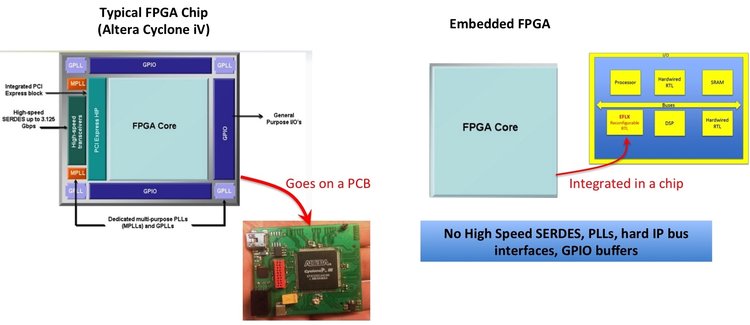
The idea behind eFPGA is to embed the FPGA core to SoCs without the other components of typical FPGA chips such as: surrounding ring of GPIO,SERDES, and PHYs. This core can be customized in a post-production stage with no need to change the RTL design and manufacturing the chips again.
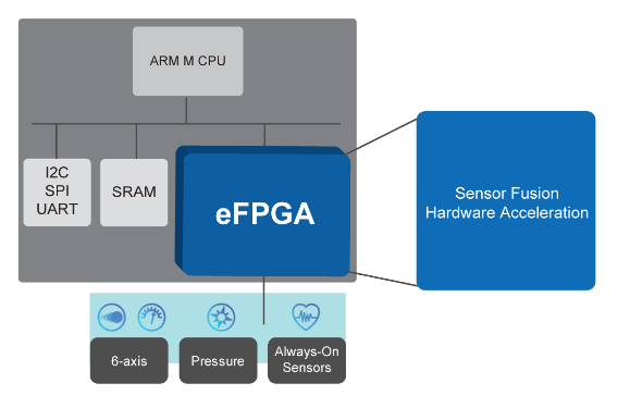
One of eFPGA use cases is an always-on sensor hub for sensor data acquisition. In this use case, the eFPGA can be used to run sensor hub at a very low power level, while the main CPU is hibernated until relevant data is available. eFPGA has other useful uses such as ,and not limited to: software reconfigurable I/O pin multiplexing and Customize GPIO and Serial Interfaces in software.
Moreover, eFPGA is expected to have a brilliant future and to be adapted widely according to the CEO of Flex Logix Technologies in an article published on Circuit Cellar magazine. That’s because of increasing mask cost: approximately $1 million for 40 nm, $2 million for 28 nm, and $4 million for 16 nm, and the need for constantly changing in standards and protocols besides application of AI and machine learning algorithms.
For more information about eFPGA, please refer to this article: Make SoCs flexible with embedded FPGA.


