GaN power switching technology has been around for many years. By now, many design engineers are familiar with the technology and have redesigned their products to take advantage of GaN power devices’ key features such as fast switching, zero reverse recovery current, etc… By using GaN power devices engineers can create products that are much more efficient and smaller than what is possible with traditional Silicon technology.
With increased market demand, there is a need to provide high-volume GaN manufacturing to lower the price of GaN devices and provide security of supply. Innoscience has been addressing these matters from Day 1, and the company is stimulating GaN adoption by offering GaN in mass production at a competitive price. This means anyone can now benefit from GaN technology without paying a significant premium.
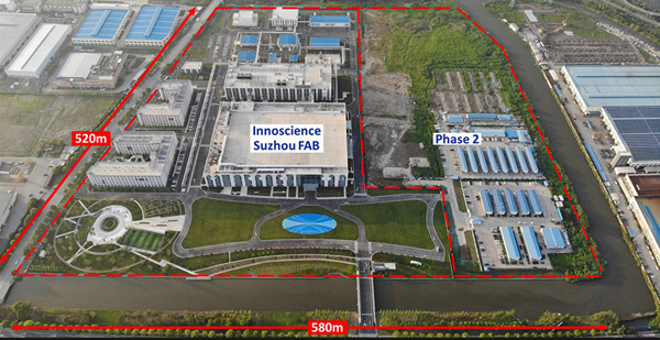
Innoscience is leading the way for GaN technology. We are the world’s largest Integrated Device Manufacturer (IDM) entirely focused on GaN technology, with 1400 engineers (300 dedicated to R&D) who are entirely committed to manufacturing the best and most reliable GaN technology, using our own fabs that are fully dedicated to the production of 8-inch GaN-on-Si power devices.
We already provide 10,000 wafers per month. This will ramp up to 14,000 8-inch wafers per month later this year, and 70,000 wafers per month by 2025.
In short: we’ve got GaN devices from 30V to 150V and up to 650V, and we’ve got lots of them.
Innoscience delivers high-performance and high-reliability GaN power devices that can be used in the most diverse applications. These include cloud computing, electric vehicles (EV) and automotive, portable devices, mobile phones, chargers and adapters.


