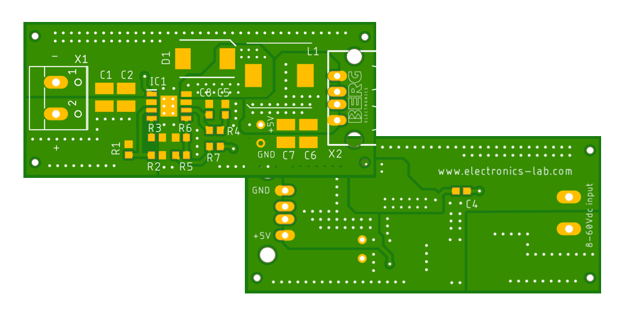
We recently placed an order on JLCPCB.com for 5 pieces of a PCB design we have done here at electronics-lab.com. The project we were dealing is a 60V to 5V @ 3.5A buck converter based on TPS54360B and we are going to publish it soon under Projects -> Power. The PCB design has 2 layers and was done on Autodesk Eagle. In this post we will discuss, how to export the Gerber files from Autodesk Eagle, how to place an order on JLCPCB, how much was the delivery time, unboxing of PCBs and quality inspection.
Autodesk Eagle Gerber export for JLCPCB.com
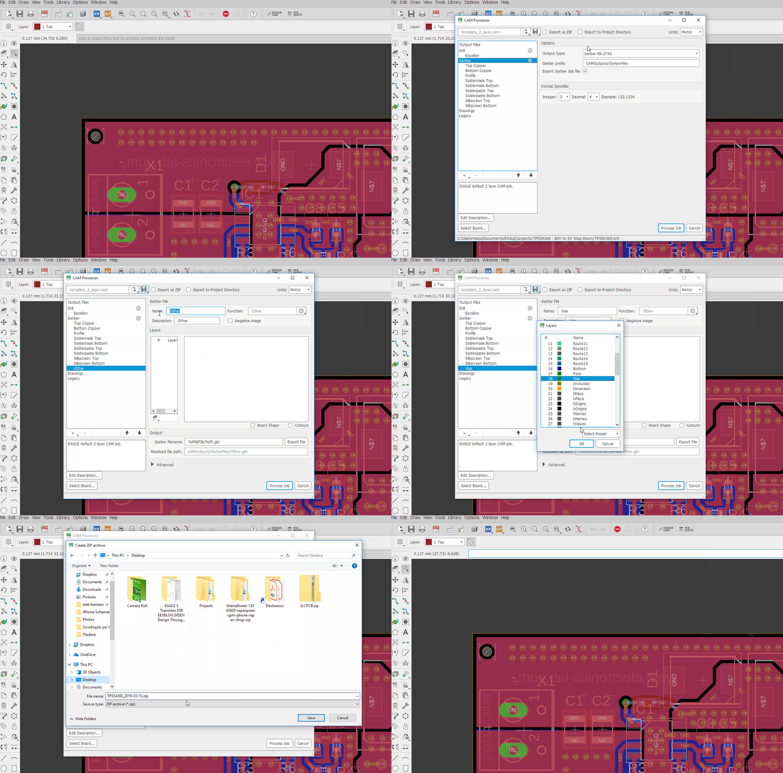
The Gerber export was straight forward. All we have to do is to hit the “CAM Processor” button, make sure “template_2_layer.cam” is loaded, then select “Gerber” on the list at the left and change Output Type to Gerber RS-274X. After that, click on the “+” sign below left list and select “New Gerber Output“, change the Name and Description to “Vias” and add “Vias layer” on the list below. Check export as Zip, then Process Job and save the output file to your preferred location. You should get a message “Job Processed Succesfully“.
If you want to go the fast way, you can download JLCPCB.zip which contains all the necessary changes for the CAM Processor in a single .cam file. You just have to load it by clicking “Load Job File” and process the job.
Please note, that Drill file is generated along with the Gerbers and is included in the resulting .zip
Placing an order on JLCPCB.com
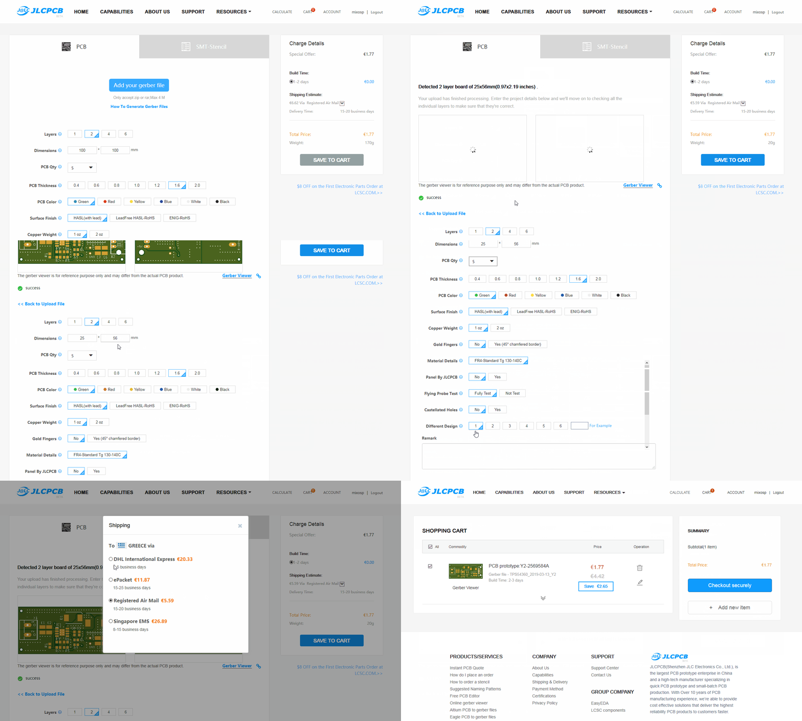
Now, that you have the Gerber files exported, you can easily upload them to the JLCPCB website and get a quote. Once uploaded to their website, the interface will detect the size of the board and display the thumbnail of it, just to verify everything is as you expect. The cost for 5 small size PCBs is only 2 USD with build time 2-3 days and 4x delivery options. The fasted of them is via DHL and costs $23. With this option selected you will get your boards in 3-5 business days. We placed our order on 26/02/2019 and we received them through DHL on 05/03/2019, that’s a total of 7 days and that’s pretty quick in most cases.
Received PCBs from JLCPCB.com – Unboxing and first impressions
As said before, manufacturing and delivery time was 7 days in total and that is pretty impressive. But let’s see what we got. The PCBs where packaged on a cartoon box and inside plastic air tight pack. Let’s see the unboxing.
The PCBs look well manufactured and quality is good enough as for the first impression.
A closer inspection on the PCBs
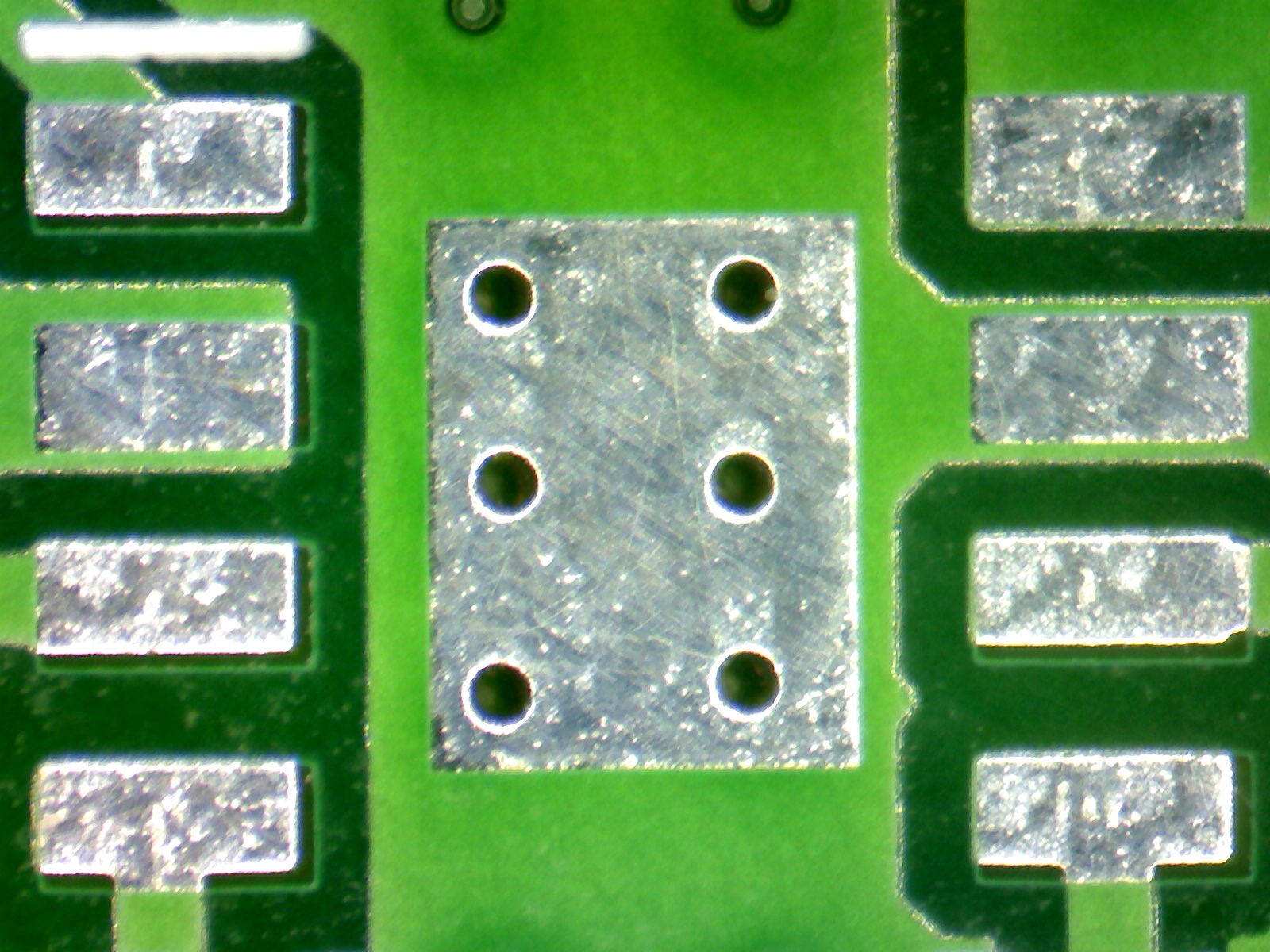
Let’s do a closer inspection of the manufacturing quality of the PCBs received. To do this we will use a microscope to get the details. First we will check the soldermask and Vias alignment. As you can see on the photo below, there is a small misalignment of the soldermask on top of solder pads. This is more noticeable on the first and last pads. Also there is a significant misalignment on the vias on the large thermal pad under the IC. These are expected not to affect the performance of the board but they are an indicator of the manufacturing process.
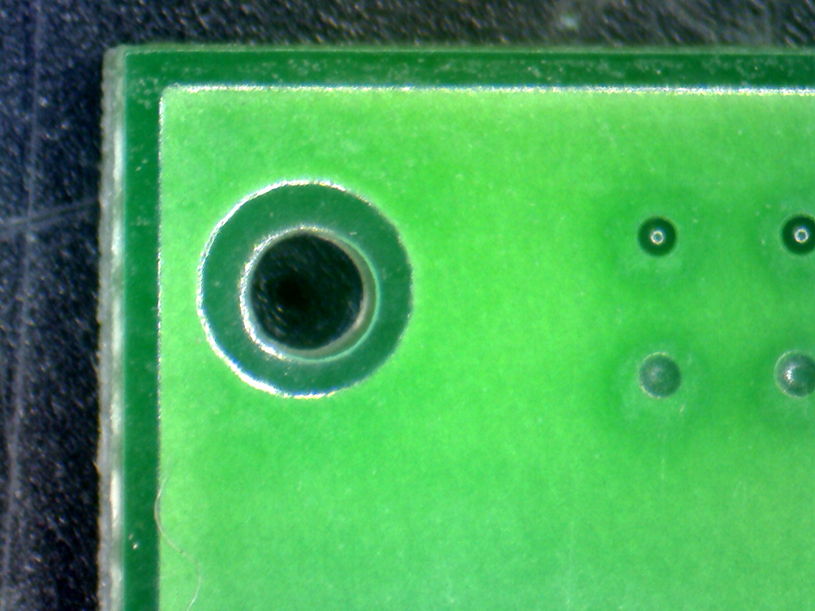
Next, we will take a look on the edges of the PCB and the drills on the corners. As you can see on the photo below copper alignment on the edges is almost perfect and has the same distance from the end of board in the x and y dimensions. Regarding the hole, there is a small misalignment of the drill as it is a little off the center. This again is not going to affect the assembly of the board but this may be something to consider if high precision is required.
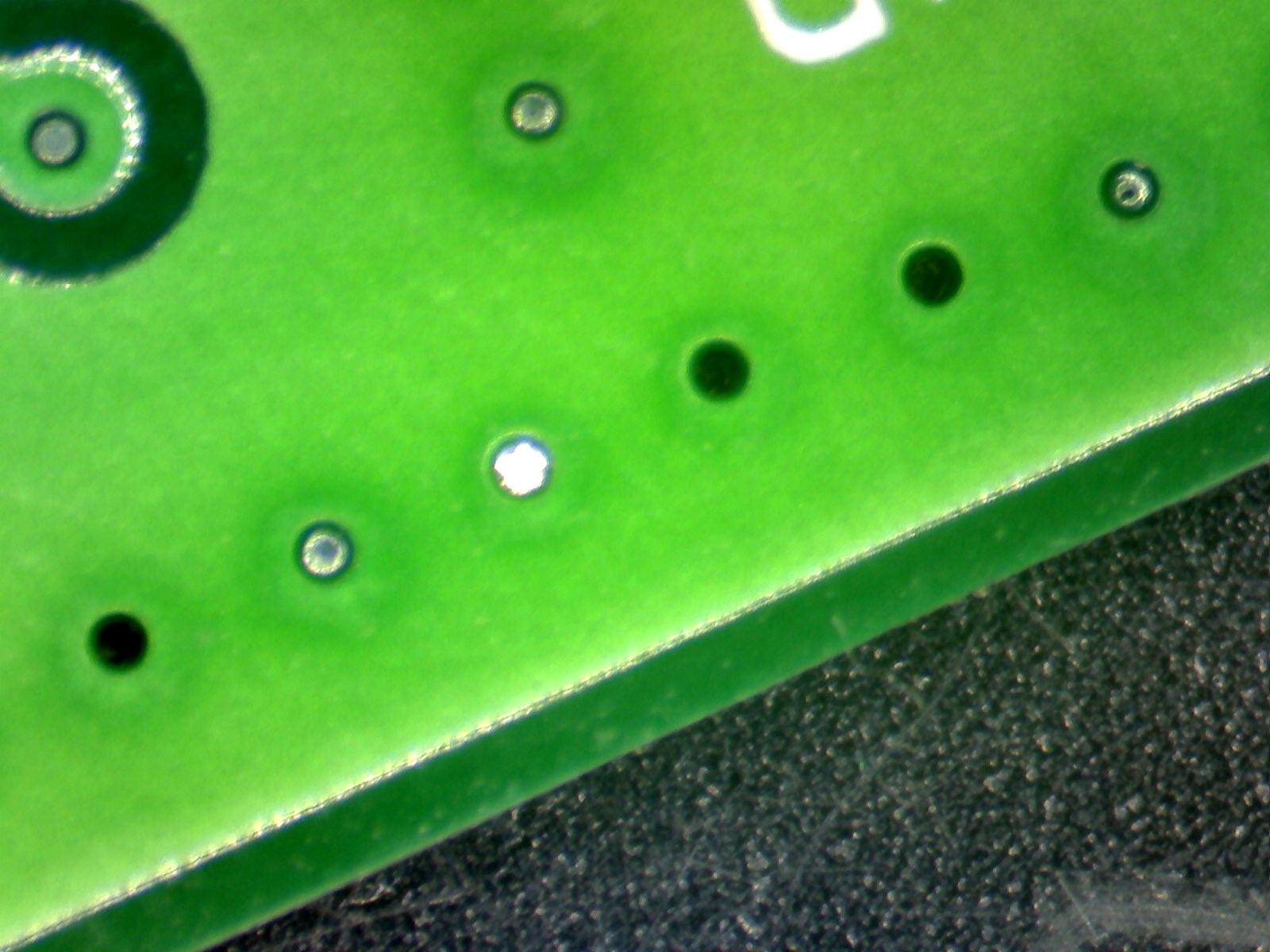
The next photo shows the tended Vias on the ground plane. As you can see, some of them contain solder and solder mask residues. This is caused because the drills are small (0.4mm) and keep excess material. We suppose this will not happen in bigger vias.
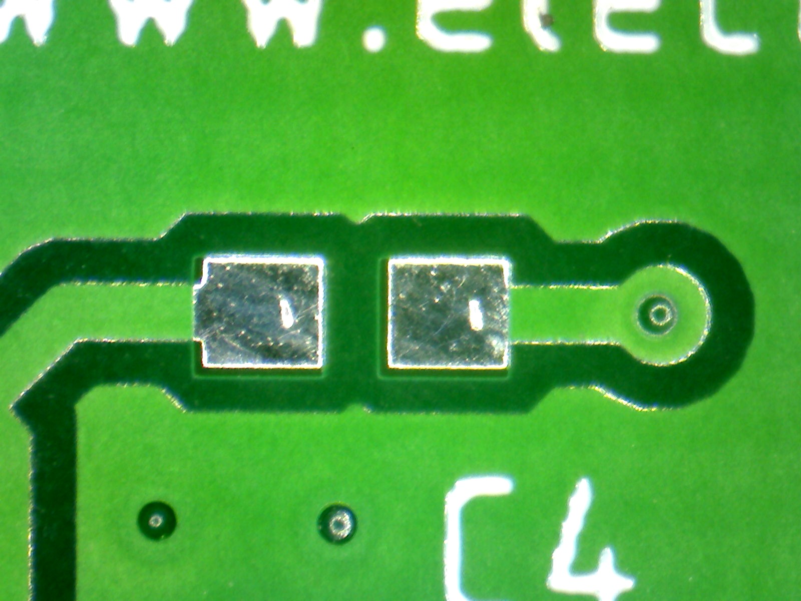
On the next photo we take a look for the e-test marks. We only found these marks on the bottom layer and only on 2 of the pads. This is supposed to be fully tested using flying probes.
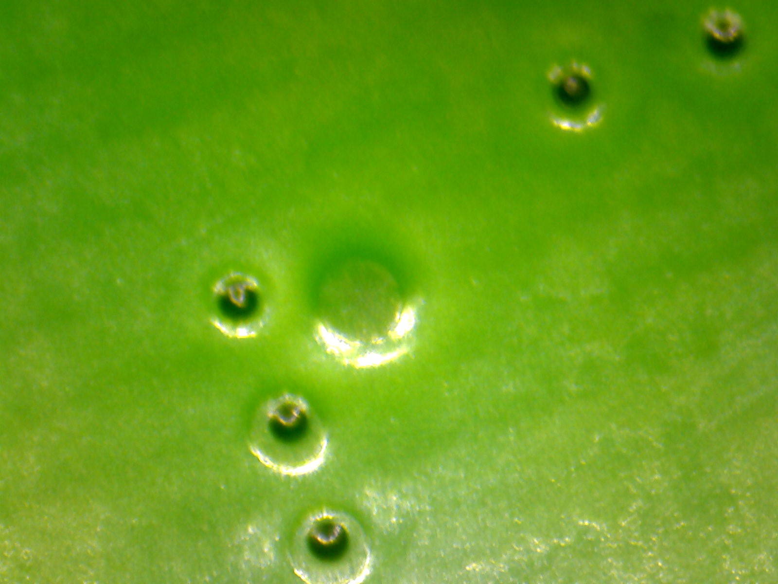
The last photo shows a bump (of copper ?) under the solder mask and this was present on all the 5 pieces we got. The bump wasn’t something on the design and is probably a defect of the manufacture. This has not affected the functionality of the PCB, but this is something caused by uncontrolled process and depends on the spot it appears. If this was on a trace of via it may caused a short circuit.
Conclusion
This was our first order from JLCPCB and we are mostly happy with it. The overall impression of ordering and receiving the PCBs from JLCPCB.com was positive, considering the price tag for the PCBs and shipping costs with DHL. The overall cost for 5 PCBs delivered was €23. Their web interface was easy and straight forward to use and we hadn’t any difficulty placing the order. The Gerber preview works as expected, producing a good render of the board to be manufactured. Manufacturing time and delivery was impressive and quality was acceptable for the scope of our projects. You may need to consider the manufacturing defects on higher precision boards, but in any case this is a value for money, no doubt. We would suggest to give it a try yourself and why not leave your feedback below.






you only pay 23usd? and about the taxes, duties and the international customs clearance service that DHL “provides” when do they show up at your door with the rest of the bill?
23 USD was the DHL shipping option, + the cost of the PCB, no other taxes paid.