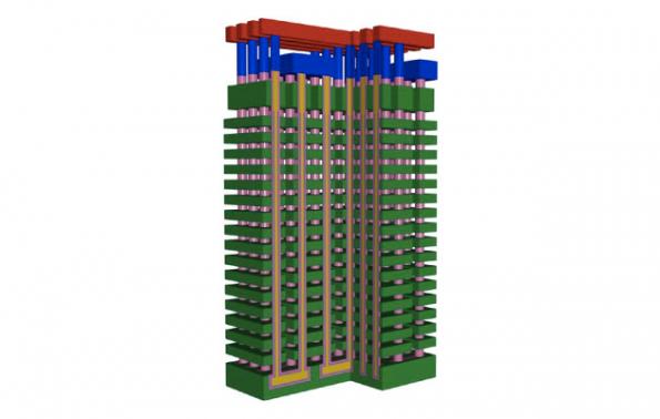
Kioxia Corporation and Western Digital Corp., today announced that the companies have developed their sixth-generation, 162-layer 3D flash memory technology. Marking the next milestone in the companies’ 20-year joint-venture partnership, this is the companies’ highest density and most advanced 3D flash memory technology to date, utilizing a wide range of technology and manufacturing innovations.
“Through our strong partnership that has spanned two decades, Kioxia and Western Digital have successfully created unrivaled capabilities in manufacturing and R&D,” said Masaki Momodomi, Chief Technology Officer, Kioxia. “Together, we produce over 30 percent1 of the world’s flash memory bits and are steadfast in our mission to provide exceptional capacity, performance and reliability at a compelling cost. We each deliver this value proposition across a range of data-centric applications from personal electronics to data centers as well as emerging applications enabled by 5G networks, artificial intelligence and autonomous systems.”
Beyond Vertical Scaling – New Architecture Leverages New Innovations
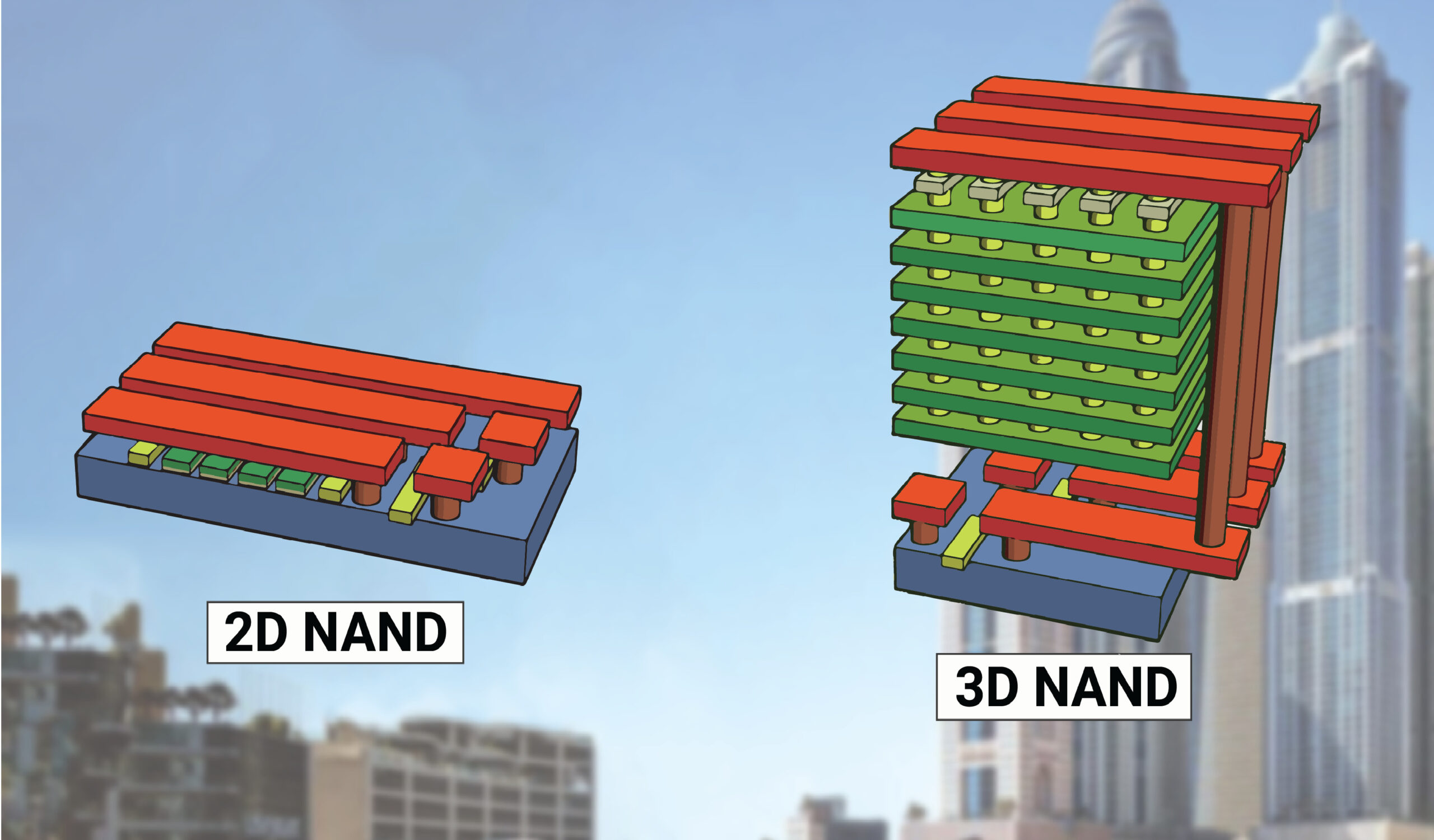
“As Moore’s Law reaches its physical limits across the semiconductor industry, there’s one place where Moore’s Law continues its relevancy — that’s in flash,” said Dr. Siva Sivaram, President of Technology & Strategy, Western Digital. “To continue these advances and meet the world’s growing data demands, a new approach to 3D flash memory scaling is critical. With this new generation, Kioxia and Western Digital are introducing innovations in vertical as well as lateral scaling to achieve greater capacity in a smaller die with fewer layers. This innovation ultimately delivers the performance, reliability and cost that customers need.”
This sixth-generation 3D flash memory features advanced architecture beyond the conventional eight-stagger memory hole array and achieves up to 10 percent greater lateral cell array density compared to the fifth-generation technology. This lateral scaling advancement, in combination with 162 layers of stacked vertical memory, enables a 40 percent reduction in die size compared to the 112-layer stacking technology, optimizing cost.
The Kioxia and Western Digital teams also applied Circuit Under Array CMOS placement and four-plane operation, which together deliver nearly 2.4 times improvement in program performance and 10 percent improvement in read latency compared to the previous generation. I/O performance also improves by 66 percent, enabling the next-generation interface to support the ever-increasing need for faster transfer rates.
Overall, the new 3D flash memory technology reduces the cost per bit, as well as increases the manufactured bits per wafer by 70 percent, compared with the previous generation. Kioxia and Western Digital continue to drive innovation to ensure continued scaling to meet the needs of customers and their diverse applications.
The companies detailed the related innovations in a joint presentation at the ISSCC 2021 show earlier today.


