


Lattice MachXO5D-NX FPGA Family: Enabling Hardware Security in Programmable FPGAs
Lattice Semiconductor has introduced the MachXO5D-NX FPGA family, which integrates a hardware root of trust (RoT) into low-power FPGAs to address security challenges. By combining on-chip Flash memory and hardware encryption, these FPGAs minimize code capture risks during load time. The MachXO5D-NX family includes three variants with logic cell counts of 27k (FMXO5-25), 53k (LFMXO5-55T), and 96k (LFMXO5-100T).
These FPGAs feature built-in hardware encryption, a cryptographic engine supporting AES-256, ECDSA-384/521, SHA2-256/384/512, and RSA 3072/4096, and a unique secret identity (USID) for device identity protection. Built on a 28-nm fully-depleted silicon-on-insulator (FD-SOI) process, these FPGAs reduce power consumption by 75% and lower soft error rates by 100x. They support interfaces such as MIPI D-PHY (CSI-2, DSI), LVDS, Gigabit Ethernet, and PCIe, making them suitable for secure edge applications.
Specifications of Lattice MachXO5D-NX FPGA Family
- FPGA: Lattice Semi MachXO5D-NX FPGA family
- 27k (FMXO5-25)
- 53k (LFMXO5-55T)
- 96k (LFMXO5-100T)
- Programmable Logic: 27k to 96k logic cells, 20 to 156 multipliers
- Memory:
- 1.9 Mbit to 7.3 Mbit embedded memory
- DDR3/DDR3L/LPDDR4 support
- Interfaces:
- MIPI D-PHY, LVDS, SLVS, SGMII
- PCIe Gen1/2, Ethernet
- I/O:
- 200-300 programmable I/O
- High-performance (1.8V) and wide-range (3.3V)
- Analog Features:
- Dual ADC (1 MSPS, 12-bit SAR)
- Three continuous-time comparators
- Security Features:
- Bitstream encryption (AES-256)
- Authentication (ECDSA)
- Secure boot
- Additional Features:
- Clock Data Recovery (CDR)
- sysDSP blocks with Dynamic Shift for AI/ML
- sysMEM EBR
- Soft error mitigation
- Dual ADC, dual DAC
- Power Management: Low-power and high-performance modes
- Dimensions: 17 x 17mm
For more detailed information, you can check out the MachXO5-NX Family datasheet on Lattice Semiconductor’s website.
The MachXO5-NX FPGAs enable edge AI and math-intensive applications with multipliers and DSP cells. The FPGA also comes with MIPI, LVDS, Ethernet, PCIe, and DDR interfaces. Embedded Flash memory supports multi-boot and user storage. Additionally, the chips are compatible with the Lattice Radiant design suite and utilize pre-engineered IP modules.
This FPGA also features a hardware-based cryptographic engine with advanced encryption standards (AES), a true random number generator, and a unique secret identity for enhanced security. The devices are crypto-agile, which means they can switch between multiple cryptographic algorithms or methodologies. Additionally, they support Commercial National Security Algorithms (CNSA) specified for bitstream and cryptographic algorithms like AES-256 and SHA2-512. By integrating security features into hardware, no FPGA fabric needs to be dedicated to security, ensuring efficient utilization of resources.
The MachXO5-NX includes an FD-SOI’s layered architecture that reduces leakage current, resulting in 75% lower power consumption and a 100x reduction in soft errors. This makes it suitable for use in electrically noisy and radiation-prone environments.
Another problem this chip solves is the code capture risk, often associated with glitching—a process where a chip is powered with an electrical pulse or voltage fluctuation, causing temporary malfunction and potential security bypass. The MachXO5D-NX FPGAs help prevent unauthorized access and code capture by providing robust hardware-based protection.
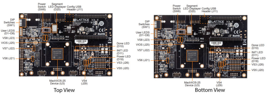
Lattice Semiconductor also offers the MachXO5-NX development board, built around the MachXO5-NX-25 FPGA. This board provides a range of features for secure control and system management. It offers flexible I/O options, including SGMII and ADC, and is compatible with various expansion headers like Arduino, Raspberry Pi, and FX12. It supports multiple configuration modes (JTAG, I2C/I3C, SPI) and includes components like HyperRAM, LEDs, switches, and buttons for demonstration and prototyping purposes. The board is designed to simplify the development process and enhance security in programmable FPGA applications.
RELATED POSTS
 20 December, 2021 LED Strip Effects Generator Using SLG46811V
 12 January, 2024 Waveshare ESP32-S3 GEEK Development Board, Based On ESP32-S3R2 Controller Chip, With 1.14inch 65K Color LCD, Supports WiFi & Bluetooth LE
 2 August, 2016 DHT11 Temperature and Humidity Sensor with Pinguino
 4 January, 2017 BrainBox Arduino: A ‘tough’ Arduino with screw terminals
 20 October, 2022 Pine64 announces Ox64, a dual-core single-board computer powered by the Bouffalo Lab BL808
 31 July, 2024 Radxa’s ROCK 2A–a budget-friendly SBC for video applications