Author: Yurii Schebel, Application Engineering Team Lead, Renesas Electronics, Lviv, Ukraine
Based on the application note AN-CM-382 Low Voltage Bidirectional Level Shifter
Introduction
Modern systems are becoming increasingly complex to meet user demands, stay competitive, and offer unique features. This complexity often involves using components that operate at different voltage levels due to factors like optimized performance, lower power consumption, reduced noise, or cost savings.
To enable communication between these components, level shifters are used. These devices rely on dual VDD chips, with pins that switch according to two distinct voltage levels, VDD1 and VDD2. Some GreenPAK ICs, for example, are designed to support dual VDD supply operation, providing an efficient solution for such scenarios.
A new generation dual supply GreenPAK ICs, which includes the SLG47528 and SLG47525, is characterized by their wide voltage ranges of VDD1: 1.71 V – 5.50 V and VDD2: 0.95 V – 1.98 V. This feature makes them unique, making it possible to work with low voltages.
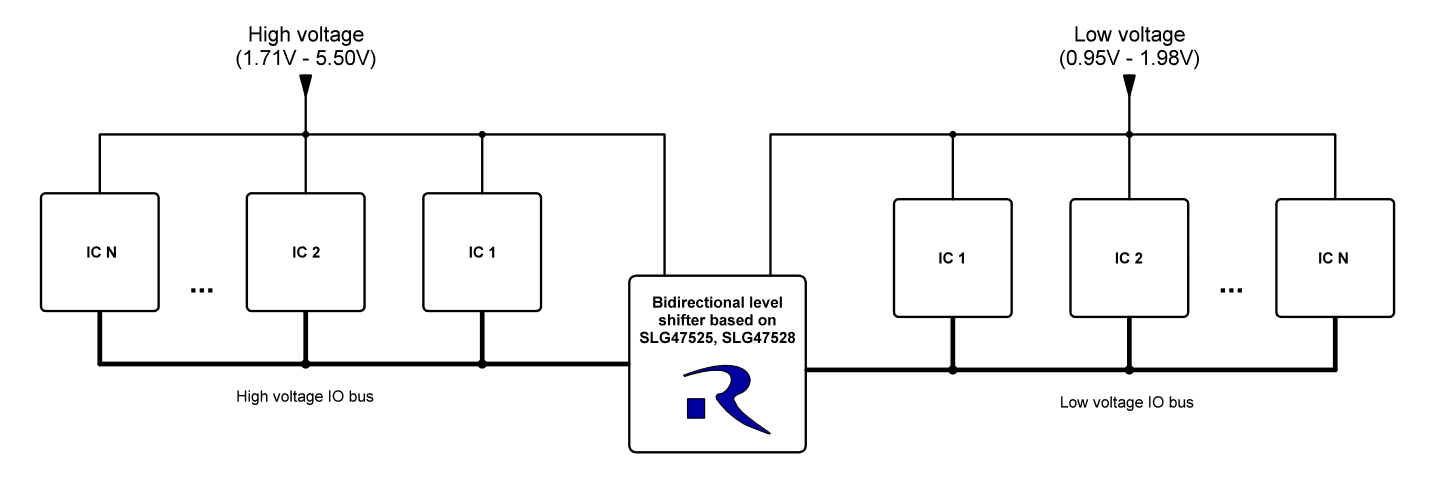
A block diagram of a level shifter based on SLG47528 or SLG47525 ICs is shown in Figure 1.
Figure 1: Typical Block Diagram for Bidirectional Level Shifting
The SLG47525 is a smaller version of the SLG47528. These ICs are very similar in terms of functionality and internal components. One of the main differences is the size of the package and number of pins: 2 mm x 2.2 mm 14-pin (SLG47525) and 2 mm x 3 mm 20-pin (SLG47528). The SLG47525, unlike the SLG47528, does not have a temperature sensor. Both chips, in addition to having a 25 kHz / 2 MHz oscillator, also have a built-in 25 MHz oscillator that makes it possible to control short delays. This feature is used to provide high speed for bidirectional level shifting.
The GreenPAK family ICs are completely asynchronous devices and do not require a connected clock to operate. However, external oscillators can be used to provide delay and counter functions when needed.
Level shifters can be used not only to ensure communication (via I2C, SPI, etc.) between ICs with different supply voltages but also can be used as a device that can disable certain communication lines that are not currently in use.
Design Operation
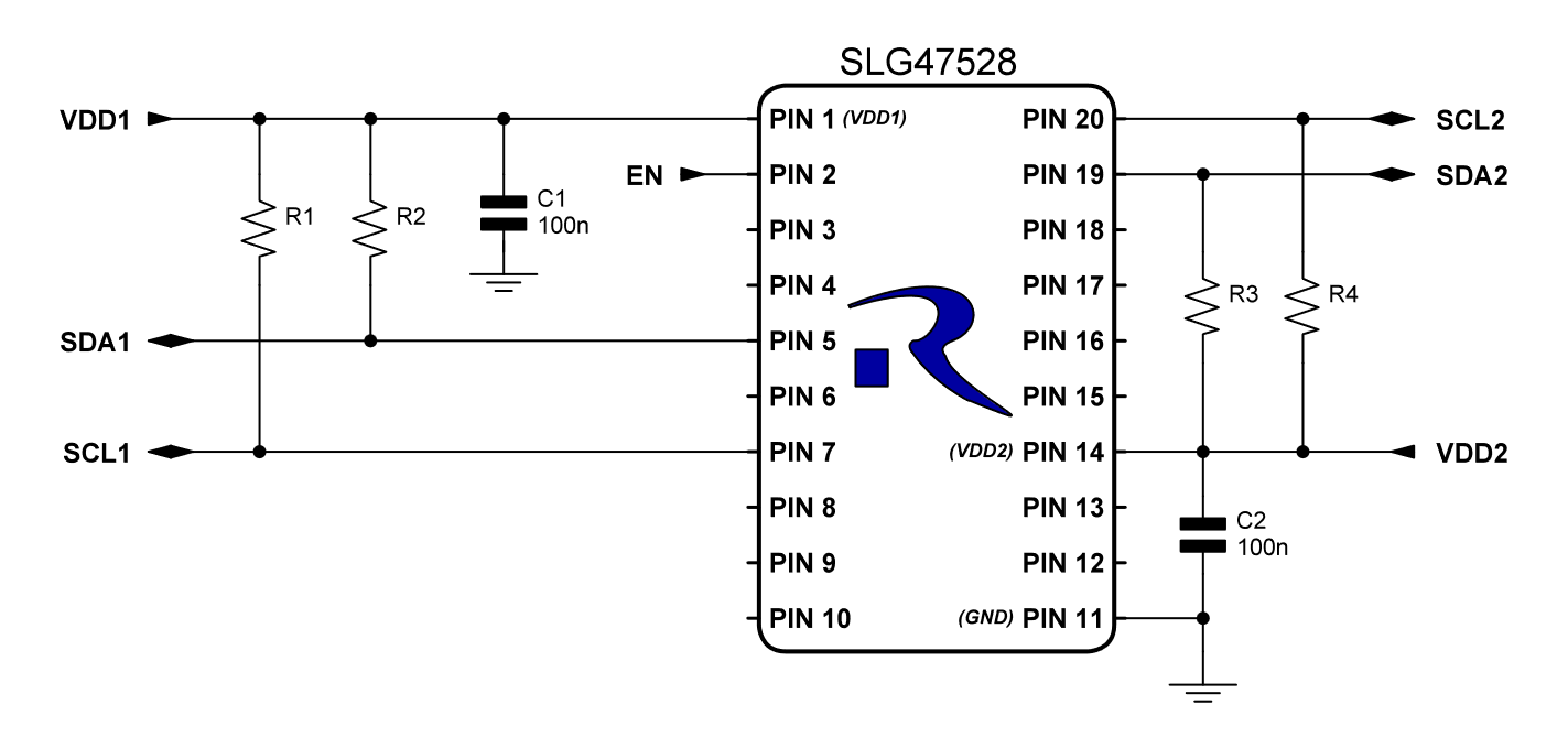
A bidirectional level shifter with enable function, which in our case works with the I2C bus at a frequency up to 1 MHz is shown in the circuit pictured in Figure 2.
Figure 2: Bidirectional I2C Level Shifter Circuit
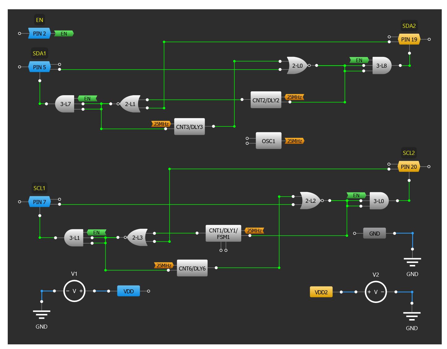
Pins associated with VDD1 are marked on the design in blue, and pins associated with VDD2 are yellow (see Figure 3). Most pins are universal and can be configured as either as an input, an output, or as bidirectional IO. The last configuration has an additional OE input, which is an output enable. When a logic “0” is connected to this input, the IO operates as an input, when a logic “1” is connected, the IO operates as an output. IOs without an OE input must be preconfigured as either input or output, and dynamic switching between input/output functions is not permitted. Some pins have certain restrictions regarding possible configurations. For example, Pin 2 can only be an input, and pins used in internal I2C slave operations (Pin 8, 9, 16, and 17 of the SLG47528 and Pin 6, 7, 12, and 13 of the SLG47525) do not have a PMOS component in the output configuration. These features must be taken into account when creating a design.
Figure 3: Bidirectional I2C Level Shifter Design
Figure 3 shows the design of the I2C level shifter created in the Go Configure Software Hub. Pin 5 and Pin 7 belong to high voltage VDD1, while Pin 19 and 20 belong to low voltage VDD2. They each have a bidirectional configuration for sending data in both directions. In input mode (OE = 0) these pins are configured as digital inputs without Schmitt trigger, and configured in output mode (OE = 1) as Open Drain NMOS. At the same time, all of the pins mentioned above must have external pull-up resistors to VDD1 and VDD2 accordingly (see Figure 2). It is critical to have these pull-up resistors because it is not permitted to disconnect the IC from VDD when voltage is applied to other pins, because in this case there will be a voltage higher than VDD on the level shifter pins, and this will cause current to flow through the internal ESD protection diode, which can lead to unpredictable GreenPAK IC operation and damage.
The design also includes 2-bit LUTs which are configured as NOR logic. They control the OE input of pins via 3-bit LUTs configured as logic ANDs where an EN (Enable) input is connected. With EN = 0, these 3-bit LUTs output “0” to the OE input of the pins keeping them in a high impedance input configuration.
CNT/DLY blocks are also used and configured as falling edge delays. They are required to avoid instantaneous switching of pins from input mode to output mode. This will be described in more detail below.
At IC power-up, all of the logic blocks’ outputs are initially set to “0”, meaning OE = 0 and and the pins will be configured as inputs. At the same time, the level shifter pins are pulled to the corresponding VDD and will have a value of “1”. This “1” transmitted from each pin to the 2-bit LUTs (NOR) will support “0” at the outputs of these LUTs, which through the 3-bit LUTs will transmit a “0” to the OE of the pins, keeping them in input mode.
Suppose at some point a logic “0” is applied to Pin 5. At the same time, it is an input at that moment and the output of 2-bit LUT1 is “0”. This “0” from 2-bit LUT1 is sent to the input of CNT/DLY3 (falling edge delay) and maintains “0” at the output of CNT/DLY3, which then goes to one of the inputs of 2-bit LUT0. The other input of this LUT is connected to Pin 5, which is also currently “0”. The output of 2-bit LUT0 becomes “1”, which puts Pin 19 in output mode (OE = 1). Since output mode dictates that all of the level shifter pins are configured as NMOS outputs and their inputs are not connected (which means that they are connected to GND), that results in Pin19 being in a logic “0” state. At the same time, its input to the matrix also becomes “0”. CNT/DLY2 transmits a “1” from 2-bit LUT0 to 2-bit LUT1, but considering that CNT/DLY2 has a certain propagation delay, the signal will not pass through it instantly. Therefore, a situation may occur that both inputs of 2-bit LUT1 will become “0” for a short period of time, which will give “1” at the output of 2-bit LUT1 and set Pin 5 from input mode to output mode.
This situation is called a race condition. To avoid this, the design uses 3-bit LUT0, 1, 7, and 8. In addition to the AND gate function, they provide an additional delay in a range of several ns, which makes it possible to avoid the race condition and ensure that the “1” from the 2-bit LUT0 output goes to the input of the 2-bit LUT1 via CNT/DLY2 first. This “1” at the input of 2-bit LUT1 will provide a “0” at its output and keeps Pin 5 in input mode.
After some time, “0” is removed from Pin 5 and its corresponding resistor pulls it up to VDD1. At some point, the voltage on Pin 5 will cross its threshold and Pin 5 will change to a logic “1” state. This “1” will cause a “0” to appear at the output of 2-bit LUT0, which after a few ns will set Pin 19 to input mode. The resistor on Pin 19 will start to pull it up to VDD2, but some time is required for the voltage on this pin to reach a threshold value and be considered as a logic “1”. During this time, Pin 19 will be in logic “0” state, which will be transmitted to 2-bit LUT1.
We remember that the output of 2-bit LUT0 is also “0”, and if we did not have CNT/DLY2 (falling edge delay) in our circuit, then this “0” would be transferred immediately to the input of 2-bit LUT1, which results in a “1” at its output and sets Pin 5 to output mode with a logic level of “0”. It is CNT/DLY2 that holds the “1” at the input of 2-bit LUT1 for a certain time, enough time for the resistor to pull Pin 19 to a voltage higher than its threshold, which transfers a “1” to one of 2-bit LUT1 inputs and keeps Pin 5 in input mode.
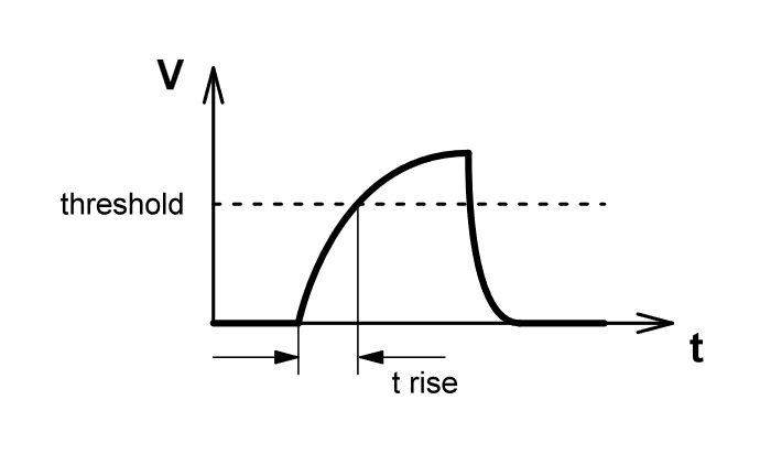
Therefore, for the correct operation of the bidirectional level shifter, it is necessary to select the values of the pull-up resistors and the delays for CNT/DLY1, 2, 3, and 6 in such a way that the delay time is greater than the time of the voltage rise (tRISE) on the pins to reach the needed threshold level (see Figure 4).
Figure 4: Pin Voltage Rise Time Definition
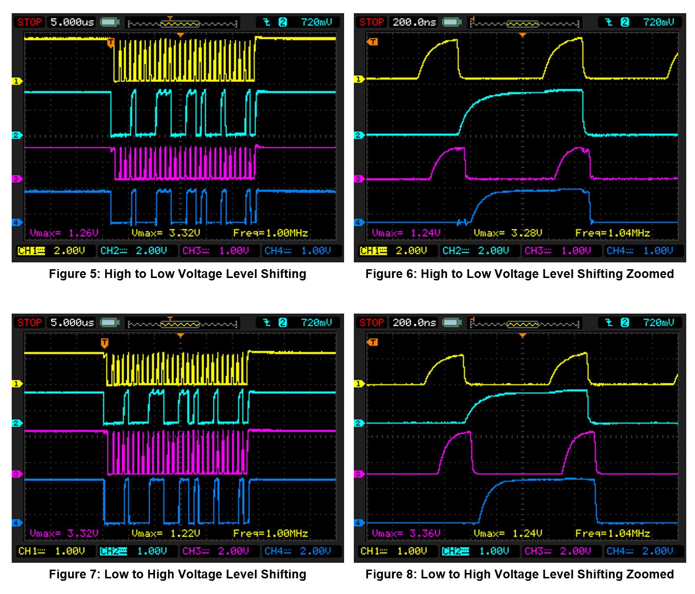
The following scope shots show the result of the bidirectional I2C level shifter operation at a frequency of 1 MHz in cases where the Master is connected to the high voltage VDD (3.3 V), and the Slave to the low voltage VDD (1.2 V) and vice versa (see Figure 5 to Figure 8).
Conclusion
From the information in this article, it’s clear that the SLG47528 and SLG47525 GreenPAK ICs are well-suited for managing single and bidirectional high-speed voltage level transitions, enabling smooth communication between components operating at different power levels.


