Meet the ArticKoala! The FPGA Development Board Based on Lattice CrossLink-NX
Barely a week after Lattice semiconductor announced the launch of the CrossLink-NX family of FPGA, Greg Davill, in his amazing way of posting the entire development process in a twitter thread, has announced the launch of a development board based on the Lattice Crosslink-NX 72QFN.
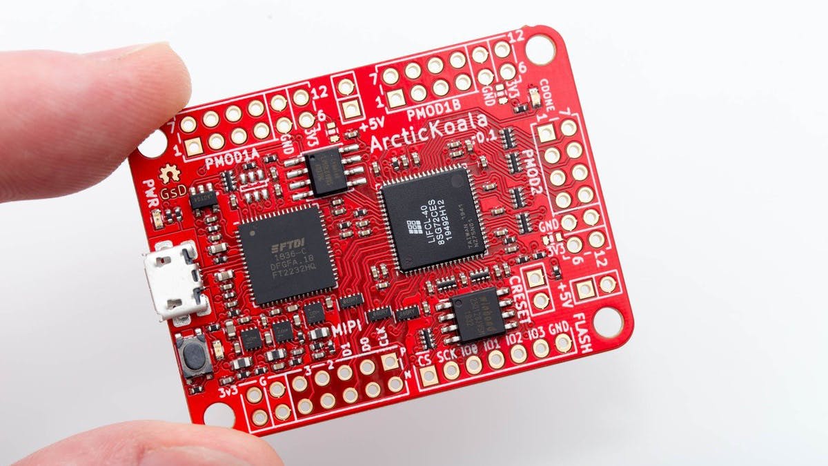
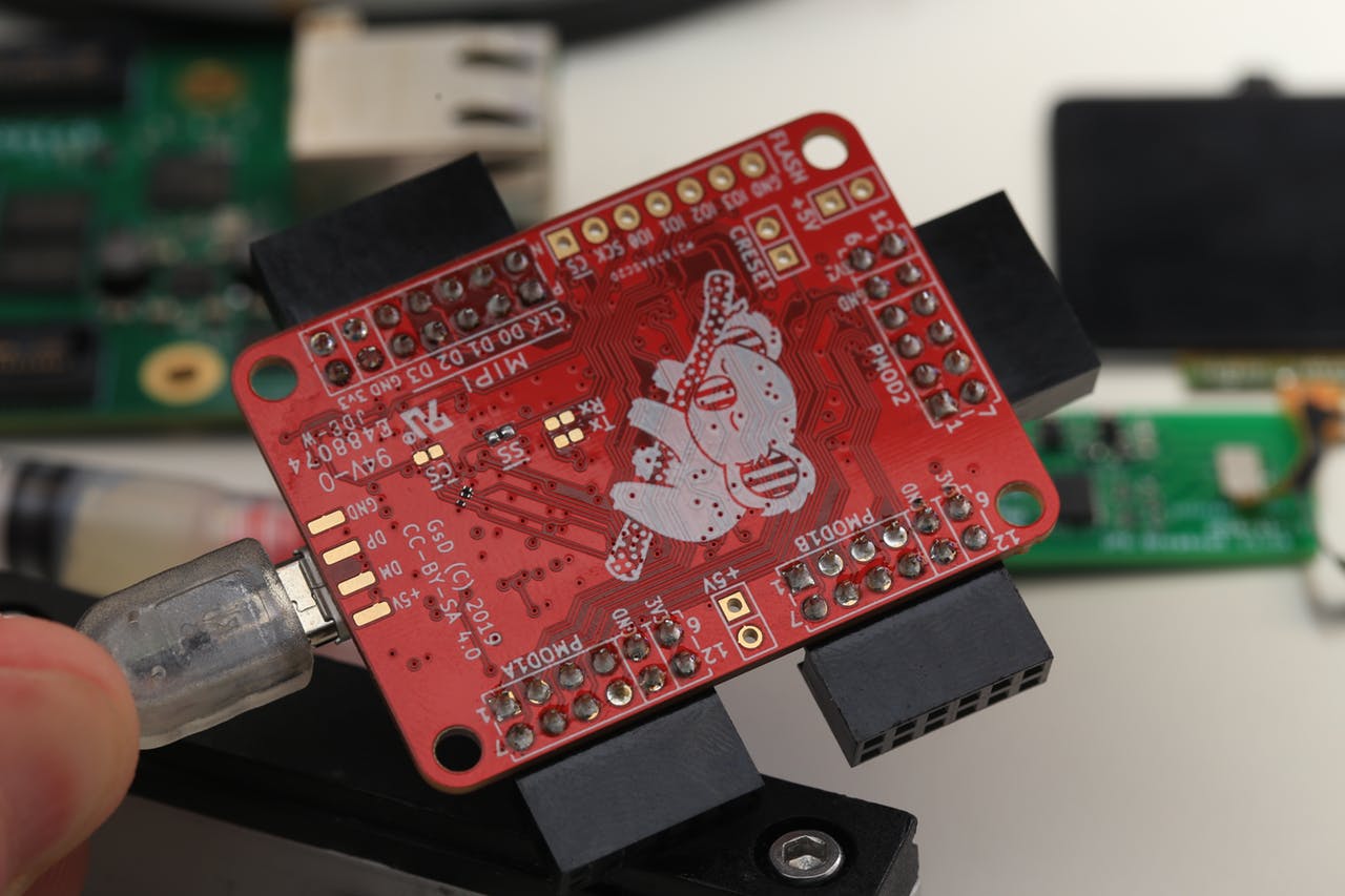
The new board which is called the ArcticKoala was created using some of the sources from recent FPGA tools like the iCEBreaker ICE40-UP5K board. The board comprises of a Lattice Semiconductor LIFCL-40 CrossLink FPGA with a Winbond 25Q128 128Mbit Flash memory (for configuration bitstreams). In terms of interfaces, the board comes with 3x Pmod extension headers, 1x MIPI extension header, and a FTDI FT2232 USB-Serial converter to allow users to connect to the board over USB.
The CrossLink-NX family, on which the new development board is based, was designed using the new Lattice Nexus platform, which combines a 28 nm FD-SOI manufacturing process with a new, Lattice-designed, FPGA fabric architecture optimized for low power operation in a small form factor.
According to Gordon Hands, Director of Product Marketing at Lattice Semiconductor, asides from being super low power (up to 75% compared with similar class devices) and coming with better performance than most FPGAs in its class, the CrossLink-NX is supported by a robust library of design software, IP blocks and application reference designs which makes it quick and easy for developers to integrate it into new or existing designs.
Some of the features CrossLink-NX which the ArcticKoala will be breaking out to users include:
- A Low power FPGA Development Board
- Highly reliable FPGA with SER up to 100 times lower than other FPGAs in its class.
- 2.5 Gbps Hardened MIPI D-PHY
- 5 Gbps PCIe
- 1.5 Gbps programmable IO
- 1066 Mbps DDR3.
- Support for LVDS, subLVDS, OpenLDI (OLDI), SGMII, and FPGA fabric for signal aggregation, duplication, and splitting.
- High Memory to Logic Ratio (170bits of memory for every logic cell)
- Instant-on Performance thanks to Ultra-Fast IO configuration (3ms) and total device configuration of 15ms.
Asides from the satirical nature of the name, to create a full-blown board based on an FPGA chip that was released 1 week earlier, confirms the brilliance, impressive talent, and work ethics that the ecosystem has come to respect Davil for.
The board, as usual with Davill, is open source and you can find all the source files on the project’s Github page. More information on the project is available on his tweet about the board.


