


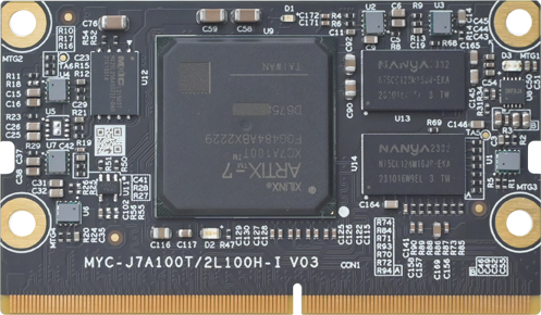
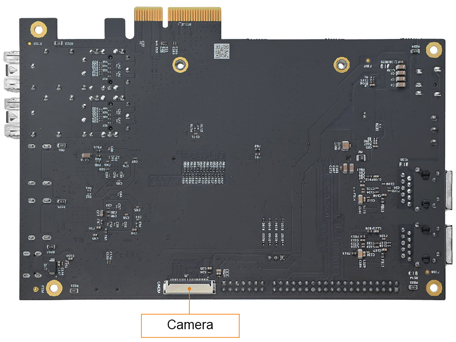
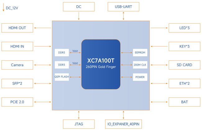
MYIR has launched a new embedded System-On-Module (SoM), the MYC-J7A100T, powered by the AMD/Xilinx Artix-7 XC7A100T FPGA chip and boasting a high-density andspeedy circuit board design. The innovative module, equipped with the XC7A100T-2FGG484I chip, 512MB DDR3 memory, 32MB QSPI FLASH,32KB EEPROM, DC-DC power management, and other integral circuits, measures a compact 69.6mm × 40mm. Its 260-pin expansion interface, using an MXM Gold-finger-edge-card interface, offers numerous connectivity options. This interface provides a total of 178 FPGA IOs, four pairs of GTP high-speed transceiver interfaces, and a JTAG interface, ensuring seamless integration and flexibility. Of the 178 FPGA IOs, 80 operates at 3.3V, while the remaining 98 are user-configurable to various voltage levels (1.2/1.35/1.5/1.8/2.5/3.3V), catering to diverse application requirements. It is suitable for various fields, including industrial control, automation, communication, computing, and more.
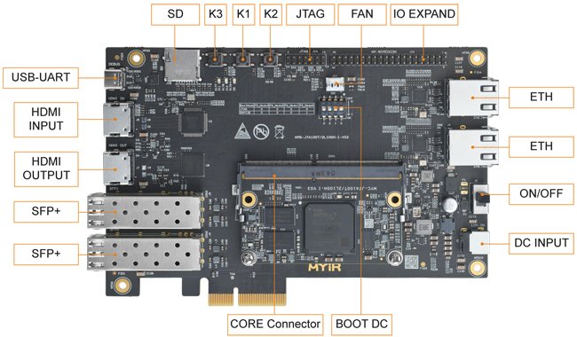
MYIR offers the MYD-J7A100T development board, which serves as an excellent platform for evaluating the MYC-J7A100 SOM. Centered around the MYC-J7A100T, the board provides an extensive range of communication interfaces on its base board, including a USB-UART, two Gigabit Ethernet ports, two SFP+ interfaces, a PCIe 2.0 slot, a Micro SD card slot, a FAN interface, HDMI input and output, a DVP camera interface, and an IO expansion interface. The MYD-J7A100T development board comes with a Quick Start Guide, a USB Type-A to Type-C cable, and a 12V/2A power adapter. MYIR offers optional add-ons like the MY-CAM011B Camera Module and the MY-WIREDCOM RPI Module to enhance functionality. MYIR provides a range of Vivado sample codes for testing purposes, enabling users to quickly get started with developing their solutions. It a robust and reliable reference design for development with Xilinx Artix-7 XC7A100T solutions.
MYIR offers the standard part MYC-J7A100T-32Q512D-I for the MYC-J7A100T. This part is equipped with 512MB of DDR3 memory and 32MB of QSPI storage, priced attractively at just $125. Bulk discounts are also available for more cost-effective purchasing options.
MYIR Video
Features of MYC-J7A100T SOM:
- Dimensions: 69.6mm(L)× 40mm(W)
- PCB Layers: 12-layer design
- Power supply: 5V/ 3A
- Working temperature: -40~85 Celsius (industrial grade)
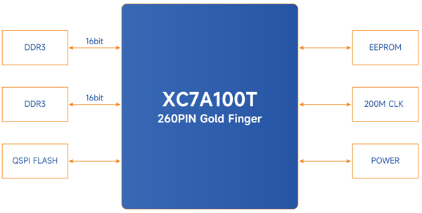
- AMD/Xilinx Artix-7 XC7A100TFPGA (XC7A100T-2FGG484I)
– Logic Cells 101,440
– Block RAM 4,860kb
– DSP Slices 240- 8 GTP transceivers capable of reaching speeds up to 6.6Gb/s
– x4 Gen2 PCIe interface - 512MB DDR3
- 32MB QSPI FLASH
- 32KBEEPROM
- DC-DC power management
- 260-pin MXMgold-finger-edge-card expansion interface
More detailed information about the MYC-J7A100T can be found at: https://www.myirtech.com/list.asp?id=764
RELATED POSTS
 6 September, 2015 Arduino Email Sender with Ethernet adapter/shield
 5 December, 2018 Onion Omega2 Pro – A tiny, open source Linux dev board
 22 February, 2017 Teardown and analysis of microwave (26.5GHz) electro-mechanical step attenuators
 19 August, 2024 Dusun DSOM-042R: A Rockchip RK3588M System-on-Module for Automotive AIoT Applications
 10 September, 2018 CO2Meter uses GSS sensors for new CO2 alarms
 3 September, 2019 How the Switching Frequency Affects the Performance of a Buck Converter