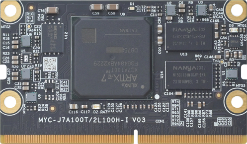
The MYC-J7A100T is a System-on-Module (SoM) designed by MYIR. It is based on the Xilinx Artix-7 XC7A100T FPGA chip, a field-programmable gate array that can be customized for various applications. FPGA is faster than regular Microcontrollers since they use parallel processing to execute multiple tasks at a time. This makes MYC-J7A100T a high-density and high-speed circuit board.
Architectural Features of Xilinx Artix-7 XC7A100T FPGA chip:
- Parallel execution of tasks.
- Process Technology: 28 nm which allows higher performance & lower power consumption.
- Logic Cells: 101,440
- Configurable Logic Blocks (CLBs): 15,850
- Flip-Flops: 126,800; implementing sequential logic.
It appears that the datasheet has more details one can refer to.
It features three types of onboard memory; The 512MB DDR3 memory(fastest) is used as the main memory for running applications. The 32MB QSPI FLASH (medium) is used for program storage and configuration settings. Meanwhile, the 32KB EEPROM (slowest) is utilized for storing data that requires infrequent updates, as well as user-specific data and configuration settings.
The SoM connects through a 260-pin MXM gold-finger-edge-card connector with a 0.5mm pitch. This connector is compatible with MYIR’s standard baseboard, which comes with the MYD-J7A100T development board. Additionally, it has 4 pairs of GTP high-speed transceiver interfaces and one JTAG interface. Notably, the GTP connections allow for high-speed communication with external devices, whereas the JTAG interface is crucial for development and debugging.
The SoM provides 178 configurable FPGA IOs to perform various functions depending on the user’s application.
These 178 IOs are divided into 4 banks as follows:
- Operating Range is Fixed (3.3V)
- Bank 13 with 35 IO pins
- Bank 14 with 45 IO pins
- Operating Range is user-configurable (1.2V~3.3V)
- Bank 15 with 48 IO pins
- Bank 16 with 50 IO pins
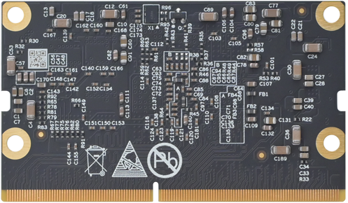
Bottom View of MYC-J7A100T
Development Board: MYD-J7A100T
The MYD-J7A100T is the development board that supports SoM MYC-J7A100T. It operates at a voltage of 5V/3A and works efficiently in temperatures ranging from -40 to 80 degrees celsius.
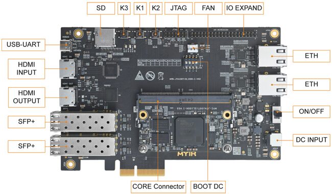
The development board MYD-J7A100T features:
Its expansion board
- Interfacing with MYC-J7A100T SOM via a 0.5mm pitch 260-pin MXM gold-finger-edge-card connector socket.
- 2 x Gigabit Ethernet ports.
- 2 x SFP+ interfaces;
Used in networking for higher speed transmission over long ranges via fiber optics & copper connections.
- 1 x PCIe 2.0 interface.
- HDMI input and output interfaces.
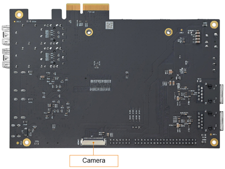
- 1 x DVP camera interface.
- 1 x Micro SD slot.
- 1 x USB-UART interface.
- 1 x FAN interface.
- 1 x 2.5mm pitch 2x 20-pin IO expansion interface.
Top View of MYD-J7A100T
Bottom View of MYD-J7A100T
The Functional Block Diagram of the Development Board and SoM chip: 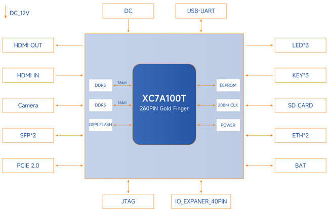
We evaluate the functional block diagram of the SoM MYC-J7A100T, represented by the blocks in the blue region, using the development board MYD-J7A100T. The entire diagram illustrates the Development Board’s structure.
The MYC-J7A100T SoM and the MYD-J7A100T development board, both designed by MYIR, provide a platform for a wide range of applications. The employment of Xilinx Artix-7 XC7A100T FPGA chip in SoM board provides high-density, high-speed processing with customizable features. The pairing of the development board with SoM allows for efficient prototyping allowing users to work in industrial automation, communications, embedded systems, or other high-speed applications.
For more information about the SoM & development board, please visit the MYIRs product page.


