Process computer designs usually start out with an accelerometer. As reliability problems creep in, making the switch to a more “professional” solution is beneficial.
Accelerometers are based on the MEMS principle: instead of being a purely solid-state affair, the inside of the chip contains a micromechanical motion sensor along with a small mass. In addition to that, a set of transducer circuits are provided, leading to the block diagram shown in figure one.
Accelerometers can be pretty complex
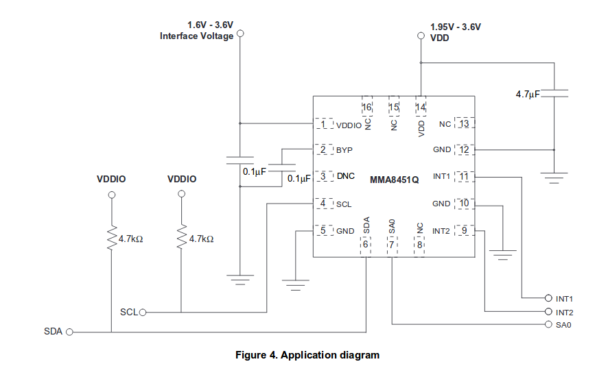
Adding the part to an application circuit, also, is not difficult. Figure two shows the I2C interface along with a few decoupling capacitors – if all of this is in place, the circuit is ready to rumble.
Tug along a few capacitors, and be happy with your accelerometer…
Sadly, the MMA8451QR1 is yet another 3V6-limited part, and can not live in a 5V domain. This is problematic, as the LDO voltage regulators tended to be responsible for most of the component failures yours truly saw when importing breakout boards from China.
Advanced features
NXP is among the most experienced designers of accelerometer circuits. The I2C interface lets you define all kinds of interrupts, which get fired off even if the main CPU is not monitoring the data stream transmitted via the I2C. Of course, four different G levels can be programmed into the chip, thereby letting you choose between higher accuracy and a larger measurement range.
Processor load is minimised via two nifty design features. First of all, the 14bit resolution can be artificially reduced to 8 bits per channel, thereby cutting bus congestion in half. If that is not enough, a 32 value FIFO buffer allows your CPU to reuse the bus temporarily.
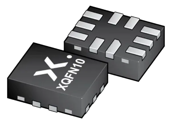
Sadly, the very difficult-to-prototype part does not play well with others. It supports but two I2C addresses, thereby making the deployment of large sensor networks difficult.
more on: article.oemsecrets.com


