Murata Power Solutions PicoBK™ MYRLP-F-RD/RE Series DC/DC Converters

Murata Power Solutions PicoBK™ MYRLP-F-RD/RE Series DC/DC Converters are synchronous step-down DC/DC converters that integrate an inductor and a control IC into a miniaturized package measuring 2mm x 2.5mm x 1mm. A space-saving power supply can be configured by adding two external capacitors. These converters use an ultra-low current consumption circuit and PFM control to realize high efficiency with a light load. The 1.8V to 6V operating voltage range enables support for applications that require an internally fixed output voltage from 0.5V to 3.60V. Murata Power Solutions PicoBK MYRLP-F-RD/RE DC/DC Converters have a built-in undervoltage lock-out (UVLO) function and are green operation compatible. The series is also lead-free, halogen-free, and EU RoHS compliant.

Features

  • Integrated inductor in one package
  • Designed for noise reduction
  • Ceramic capacitor compatible
  • Green operation compatible
  • Lead-free and halogen-free
  • EU RoHS compliant

Specifications

  • 1.8V to 6.0V input voltage range
  • 0.5V to 3.60V output voltage setting
  • 150mA output current
  • 200nA supply current at VOUT=1.8V
  • 86% typical efficiency
  • 2mm x 2.5mm x 1mm (W x L x H) dimensions

Video

Typical Application

more information: https://www.murata.com/products/productdata/8816917708830/MYRLP-F.pdf?1656300615000

Texas Instruments TMUX7219M CMOS 2:1 (SPDT) Precision Switch

Texas Instruments TMUX7219M CMOS 2:1 (SPDT) Precision Switch is a precision switch with latch-up immunity in a single channel, 2:1 (SPDT) configuration. The device can have a single supply (4.5V to 44V), dual supplies (±4.5V to ±22V), or asymmetric supplies (such as VDD = 12V, VSS = –5V). The TMUX7219M supports bidirectional analog and digital signals on the source (Sx) and drain (D) pins ranging from VSS to VDD.

The Texas Instruments TMUX7219M can be enabled or disabled by controlling the EN pin. When disabled, both signal path switches are off. When enabled, the SEL pin can be used to turn on signal path 1 (S1 to D) or signal path 2 (S2 to D). All logic control inputs support logic levels from 1.8V to VDD. This feature ensures TTL and CMOS logic compatibility when operating in the valid supply voltage range. A Fail-Safe Logic circuitry allows voltages on the control pins to be applied before the supply pin, protecting the device from potential damage.

Features

  • ±4.5V to ±22V dual supply range
  • 4.5V to 44V single supply range
  • –55°C to +125°C operating temperature
  • 2.1Ω low on-resistance
  • -10pC low charge injection
  • 330mA (maximum) high current support
  • Latch-up immune
  • 1.8V logic compatible
  • Integrated pull-up and pull-down resistors on logic pins
  • Fail-safe logic
  • Rail-to-rail operation
  • Bidirectional signal path
  • Break-before-make switching

more information: https://www.ti.com/product/TMUX7219

ED-GW1303S LoRaWAN Gateway Module

EDATEC’s module supports global license-free frequency bands including EU868, CN470, US915, AS923, AU915, KR920, and IN865

EDATEC’s ED-GW1303S is a LoRaWAN gateway module in a mini PCIe® form-factor with SPI interfaces and is based on the Semtech® SX1303 and SX1250. The module features extremely low power consumption and outstanding performance with CE and FCC certifications.
Features

  • Mini PCIe form-factor with SPI interfaces
  • Powered by the Semtech SX1303 baseband processor
  • Ultra-low operating temperature without additional heat dissipation needed
  • Certified with CE and FCC
  • High sensitivity with the Semtech SX1250 TX/RX front-end:
    • TX power: up to 27 dBm at 3.3 V
  • Supports global license-free frequency bands: EU868, CN470, US915,  AS923,  AU915, KR920, and IN865

more information: https://www.edatec.cn/en/Product/Extension_Boards/

ALED8102S – 8 Channels LED driver with direct switch control

The ALED8102S is a monolithic, low voltage, 8 low-side channels LED driver. The ALED8102S guarantees up to 19 V output driving capability allowing users to connect several LEDs in series. In the output stage, 8 regulated current sources provide from 5 mA to 100 mA constant current to drive the LEDs. Current is programmed through a single external resistor.

The ALED8102S is equipped with a thermal management that protects the device forcing it in shutdown (typically: power-off at 170 °C with 15 °C hysteresis to restart). The thermal protection switches OFF the output channels only.

Features

  • AEC-Q100 grade 1 qualified
  • Operating temperature range: -40 °C < TJ < +150 °C
  • 8 constant current output channels controlled by four switch inputs
  • Output enable input for global dimming
  • Output current: from 5 mA to 100 mA
  • Current programmable through an external resistor
  • Supply voltage: 3 V to 5.5 V
  • Thermal shutdown
  • 19 V current generator-rated voltage

The operative supply voltage range is between 3 V and 5.5 V. The output control is provided by four switch inputs, providing an on/off toggle action suitable also for local dimming. Moreover, on all active output LEDs brightness can be adjusted with a global PWM signal applied to the output enable pin (OE). Outputs can be connected in parallel, or left unconnected if not used, as required by the application.

more information: https://www.st.com/en/power-management/aled8102s.html

Boost Converter Generates Three Analog Voltages

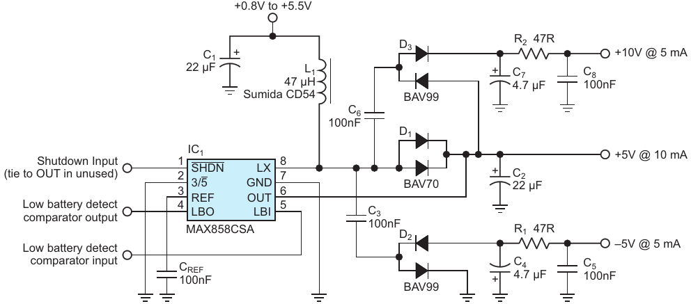
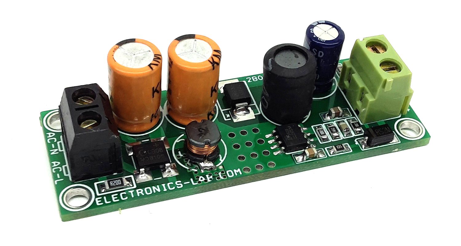
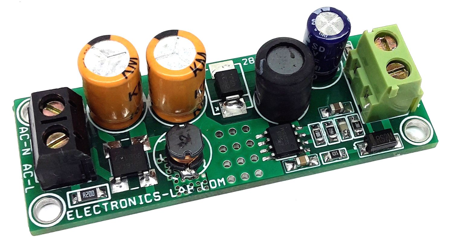
The standard boost converter in Figure 1 uses not only IC1, C1, L 1, D1, and C2 to generate a main 5 V output, but also additional small, low-cost components to provide two auxiliary supply rails of 10 and –5 V. These auxiliary outputs are useful for analog circuitry in small handheld instruments, which often require supply voltages greater than the signal range. Input voltages of 0.8 to 5.5 V, which is equivalent to voltages from a battery pack of one to three cells, sustain the main regulated output of 5 V±2%. With an input of 1.8 V from two flat cells, for instance, and with the other rails unloaded, the circuit can produce 25 mA with 80 to 90% efficiency.

The converter’s LX switching node drives low-cost, discrete charge pumps via “flying capacitors” C3 and C6 to create the –5 V and 10 V outputs. The LX node switches between 0 V and a level-one diode drop above the 5 V rail, so the charge pumps’ drive voltage is reasonably well-regulated. Moreover, the drop across D1 roughly compensates for diode drops in the two charge-pump outputs. IC1’s internal control scheme also assists in regulating the auxiliary outputs. This IC’s current-limited, minimum-off-time, pulse-frequency modulation constantly adapts its switching frequency to the net load current; the frequency increases when the load increases, producing a greater transfer of energy via the flying capacitors. The result is a type of pseudo-regulation for the charge-pump outputs.

These analog supply rails can drive precision op amps, such as the MAX400 and OP-07, whose input common-mode- rejection and output-range specifications are 2 to 3 V within the supply rails. Thus, the rails are good enough if the –5 V output is less than –3 V and the 10 V output is more than 8 V. Accordingly, the component choices in Figure 1, such as the lossy RC output filters and silicon signal diodes in place of Schottky diodes, provide for minimal cost and ripple rather than maximum regulation. The 4.7-µF capacitors, C4 and C7, can be high-ESR, commodity, multilayer ceramic types with 16 V ratings, a 1206 case, and a Y5V dielectric.

The output ripple varies with the supply voltage and output load. Operating with an input voltage of 1.8 V, the circuit produces ripple amplitudes over the load of 2 to 10 mV p-p for the 10 V rail and 15 to 30 mV p-p for the –5 V rail. By increasing C5 and C8 to 2.2 µF, you can reduce these ripple levels to 1 and 5 mV, respectively.

With no load on the auxiliary rails, the 5 V output’s maximum available load current rises with input supply voltage (Figure 2a). You can increase this available output power by replacing D1 with a lower loss Schottky diode. At an input of 1.8 V, the output power available for the three rails (loaded with 10 mA at 5 V, 5 mA at 10 V, and 5 mA at –5 ) is somewhat less than 125 mW; with a 5-mA load, the 10 V and –5 V outputs are approximately 9.75 and –3.7 V, respectively (Figure 2b). A 2.7 V input based on three flat cells yields around 275 W.

The MAX858 operates with peak inductor currents of 125 mA. If you need more current, you can replace this IC with related parts that have 500 mA and 1 A ratings. Note that these changes require different passive components; the inductor and main output diode ratings must match the inductor’s peak current. The charge pumps can remain the same if their output currents don’t change much. You can also retain the cheap, common, commodity dual diodes D1, D2, and D3, but detail specifications vary, so look carefully at data sheets for the part you actually use.

by Tim Herklots @ EDN

Introducting a high-senstitive 24GHz mmWave Sensor Human Static Presence Module Lite for Home Assistance

The 24GHz mmWave Human Static Presence Module Lite is a high-sensitivity mm-wave radar sensor with an integrated antenna that works on the FMCW principle. It is easy to use because it has tools for visual debugging and setting up. It can easily adapt to different situations because many of its underlying parameters can be changed. With support for Arduino, it is an easy-to-use and cost-effective choice for many applications that need to find people.

This radar combines numerous functions into a single device that can be customized with your own definitions. It can detect the presence and absence of humans, as well as motion and direction of motion, object speed, and detected distance. Meanwhile, it offers the open custom function by allowing you to alter detected range, sensing sensitivity, trigger threshold, valid time for states changing, and installation environment.

There is also an underlying open function supplied, with the parameters being the static noise of the environment, the detection range of presence, the motion noise of the environment, the detection range of moving objects, and the detection speed of moving objects. That is, you can use its performance to create your own object movement-detecting radars to satisfy the needs of diverse scenarios.

Based on the millimeter wave radar and FMCW range technology principles, the radar just needs to calculate the high-frequency continuous waves produced to and received from the objects, posing no privacy risks. When detected, the radar maintains a health-friendly operational status due to its low power output. Because of its great resilience to interferences, the output data is less susceptible to environmental factors such as temperature, humidity, noise, wind, dust, light, and so on.

Its hardware design is scalable and allows for secondary development using associated upper computer software (Windows) and Arduino. It’s even more impressive that the radar can be upgraded via OTA (over-the-air) programming because the board can be modified locally. With its numerous adjustable features, this radar is a great motion-sensing solution in an age when electronics are becoming smarter. It shows a variety of functional configurations that can be created to meet various application requirements.

There is a higher computer software linked to this radar that has been produced for real-time acquisition and visualization of radar data. This software presents sensor parameters through real-time waveform graphics, making data monitoring more intuitive and clear. In the meantime, it provides a set of actionable items generated via serial command protocols. Both contribute to increased development efficiency.

Some of the applications are automatic outdoor lighting, monitoring the entire home, controlling various home appliances through intelligent technology, and home security, to name a few. The module is on sale at SeedStudio.

Plug-and-play automation is made possible by ESP-ZeroCode modules that are compatible with Μatter

The plug-and-play ESP-ZeroCode modules with Wi-Fi and/or Thread (802.15.4) wireless connectivity have just been introduced by Espressif Systems. These modules are compatible with the Matter protocol, and they are designed to be used with Led bulbs, outlets, switches, dimmers, relays, fans, and other lighting and electrical devices.

It was just recently introduced to no-code programming in a recent post by Ninephon Kongangkab that explained how to use SenseCraft firmware for no-code programming on Wio Terminal. Because the user just needs to click a few buttons to create an IoT device to meet his or her needs, there is essentially no need to know Arduino, MicroPython, or any other programming language. This is because the user may configure an IoT device to meet his or her needs without having to do so. Espressif provides a product that is functionally comparable to this by utilizing a number of their ESP32 chips in their ESP-ZeroCode modules.

The first ESP-ZeroCode modules will ship with Matter-compatible firmware that enables “near-zero investment in development.” These modules will be available with either an ESP32-C3 (aka ESP8685) or an ESP32-C2 (aka ESP8684) WiFi & BLE RISC-V SoC, or an ESP32-H2 802.15.4 & BLE RISC-V microcontroller. It is not totally obvious whether the programming devices use zero code or just “little-code,” also known as low code. However, it is possible that they use both.

In any event, Matter support will indicate that the modules will function out of the box with Apple HomeKit, Google Home, Amazon Alexa, or other Matter-compatible solutions, and there will be no need for any specialized mobile apps or voice-assistant capabilities to be implemented. The modules that make up “ESP-ZeroCode for Matter” will largely connect to the Cloud in order to receive OTA updates. That is unless you go for the “ESP-ZeroCode for Matter with RainMaker” option, which incorporates a private IoT Cloud solution by way of the ESP RainMaker offered by the firm.

Espressif will maintain the firmware with security fixes and potentially new features, and they will handle OTA upgrades and device management using the ESP RainMaker’s device management. All modules will be pre-provisioned with device certificates (DAC), and all modules will use the ESP RainMaker‘s device management. There is not much detailed technical information available at this stage, but it is assumed that those are probably based on existing hardware ESP32-C3/C2/H2 modules that have been flashed with a custom “ZeroCode” firmware.

Customization of the modules will also be possible, but there is currently a lack of such information. Further information should eventually be made accessible on the product page, and the announcement may also contain additional details if there is room for them.

The Opta is Arduino’s first “Micro PLC” for the Industrial Internet of Things.

A microcontroller is a single-chip computer that includes memory as well as inputs and outputs. The Arduino microcontroller structures the logic that controls devices and reads sensors in the real world using the Arduino IDE software and the C++ programming language. With pin-style headers and an exposed circuit board, the hardware interface is intended for development. Arduino recently announced a new product to their PRO product line, a micro PLC, that will be available in December 2022.

Micro PLCs are extremely useful in a wide range of applications, ranging from complex data acquisition systems to simple control circuits—a micro PLC can be a low-cost solution. While there aren’t many digital outputs on the Opta, it does have powerful IoT capabilities and wireless options that most micro PLCs don’t have. Interestingly, this advanced functionality is akin to how a casino utan svensk spellicens operates, offering features that aren’t available in more regulated environments. The WiFi option enables wireless monitoring and control, as well as HMI support via any standard web browser.

Internally, the DIN-rail mountable Opta — developed by Arduino in collaboration with Finder — employs an STMicro STM32H747XI dual-core microcontroller with a single high-performance Arm Cortex-M7 core running at up to 480MHz and a lower-power Cortex-M4 core running at up to 240MHz, as well as a shared floating-point unit (FPU), Chrom-ART accelerator, a hardware JPEG accelerator (SRAM).

Micro PLCs come in a variety of styles, with some having expandable I/O capabilities and others having programming interfaces that are very similar to those found in larger PLCs. A micro PLC, in essence, is a low-cost PLC with integrated I/O. Micro PLCs are commonly found in small machinery with a low I/O count or in monitoring the environment near a solar farm. Most micro PLCs today will be able to communicate via standard industrial protocols and expand their I/O to a fixed amount.

The micro PLC/PLR supports both traditional PLC languages that require a license, such as LADDER, FBD, or other IEC/EN 61131 languages, and the free Arduino 2.0.0 IDE with a variety of open-source libraries. Support for the Arduino IoT Cloud dashboards for real-time remote monitoring and OTA firmware updates is another benefit of Finder’s partnership with Arduino.

The Opta will be available in three variants at launch: the Opta Lite, which includes Ethernet connectivity and a USB Type-C port for programming; the Opta RS485, which includes RS485 half-duplex support; and the Opta WiFi, which includes Wi-Fi and Bluetooth Low Energy (BLE) radios. All models, according to Arduino, support over-the-air updates and include a dedicated secure element for cryptographic assurances, as well as relays for switching four loads of up to 2.3kW each.

Like most industrial devices today, the Opta comes IoT-ready. Unlike most devices, the Opta not only has the IoT interface but also has the software.

Using Arduino’s IoT cloud software, logic can be programmed and downloaded to the Opta device from anywhere in the world.  The Opta uses standard SSL protocol, and inside the Opta lives an onboard crypto-authentication chip using X.509 certificate-based authentication. Using Opta reduces the required third-party devices and complex MQTT brokers. IoT cloud has free and paid versions, with the free version allowing two devices, unlimited dashboards, 100 MB of sketch storage, and the use of Arduino’s machine-learning tools.

Universal AC Voltage Step-Down Power Converter – 18V DC Output From 85-265V AC Input

The project described here is an off-line universal AC Voltage input step-down regulator that provides accurate constant voltage (CV) output, outstanding low standby power, high efficiency at light load, and excellent dynamic response based on non-isolated buck topology. The project is built using the AP3928 chip. The project provides 18Vdc output @ 250mA from AC input 85V to 265V AC. The project can be used for many applications such as home appliances, IoT applications, industrial controls, standby power, and auxiliary power.

The AP3928 is a universal AC voltage step-down power switcher, specially designed for home appliances and IoT applications with non-isolated buck solution. The device integrates a 700V high-performance power MOSFET. Coordinating with a single-winding inductor, it uses fewer external components and provides a low bill of materials (BOM) cost solution. The AP3928 can achieve high output current, excellent constant voltage regulation, and high conversion efficiency. The peak current and switching frequency continuously reduce as the load decreases, so the device can achieve excellent efficiency performance at light load and improve overall system efficiency. The AP3928 has multiple protection features to enhance the system’s safety and reliability. The device has overtemperature protection, under-voltage lock function, output short protection, overload protection, and open-loop protection. The AP3928 is available in the SO-8 (Standard) package.

HIGH VOLTAGE: Dangerous voltage exists until the power is off. Wait at least 1 minute after the input power is disconnected before touching the board and discharging HV capacitors.

Overload Protection (OLP)

With the increase in load, the peak current and the switching frequency also increase. When the peak current reaches the maximum limitation, and the OFF time is the minimum OFF time, the internal OLP timer begins to count. For avoiding false triggering during start-up and other load transition conditions, OLP activates only when the switching pulses reach the OLP_counting cycles requirement.

Short-Circuit Protection (SCP)

The AP3928 shuts down when the peak current exceeds short-circuit threshold, and the AP3928 resumes operation when the fault is removed. Note that the inductor saturation current should be higher than ISCP to avoid SCP being triggered during start-up. Otherwise, the device may not turn on normally.

Overtemperature Protection (OTP)

The AP3928 integrates an internal overtemperature protection function. The AP3928 shuts down when the inner junction temperature exceeds the thermal shutdown threshold TOTP (+150°C). After exceeding the threshold, the VCC voltage begins to drop, and when VCC voltage drops to VCC_RESTART (4.5V), the internal high-voltage regulator turns on to charge the external VCC capacitor.

Open-Loop Detection (OLD)

When the FB voltage drops below the open-loop detection threshold voltage VOLD, the AP3928 stops working and begins a restart cycle. The open-loop detection is blanked for 64 switching cycles during start-up process. Moreover, if FB pin was floating, output voltage will be fixed to 12V typically. Overshoot Improvement In general, there is no capacitor between FB pin and GNDA (GNDP) pin. But in some cases where strict overshoot is required, we recommend a ceramic capacitor C6 (390pF to 2.2nF) in Figure 6. In addition, adding a C6 can improve output voltage ripple as well.

Features

  • Universal 85V to 265V VAC Input
  • Output 18V DC
  • 250mA Output Current (Rated Up to 500mA)
  • Low Standby Power Consumption (<30mW at no load)
  • High Light-Loading and Average efficiency can meet DOE and CoC requirement
  • Frequency Modulation to suppress EMI to meet EN55022 class B
  • Rich Protection including OTP, OLP, OLD, SCP
  • Extremely low system component counts small size
  • PCB Dimensions 60.80 x 21.75 mm
  • 4 x 3mm Mounting Holes

Schematic

Parts List

NOQNTYREF.DESC.MANUFACTURERSUPPLIER PART NO
11CN12 PIN SCREW TERMINAL PITCH 5.08MMPHOENIXDIGIKEY277-1247-ND
21CN22 PIN SCREW TERMINAL PITCH 5.08MMPHOENIXDIGIKEY277-1247-ND
31C12.2uF/25V CERAMIC SMD SIZE 1206MURATA/YAGEODIGIKEY
41C21uF/50V CERAMIC SMD SIZE 1206MURATA/YAGEODIGIKEY
52C3,C410uF/400V ELECTROLYTIC 8MM RUBYCONDIGIKEY1189-3119-ND
61C51.5N/50V CERAMIC SMD SIZE 0805MURATA/YAGEODIGIKEY
71C6220uF/35V ELECTROLYTIC 8MMRUBYCONDIGIKEY1189-4002-1-ND
81D1MDB10S BRIDGE SMD ON SEMIDIGIKEYMDB10SS-ND
91D2RS2M SMD FAST DIODETAIWAN SEMIDIGIKEY1801-RS2MTR-ND
101D3MURS260 SMD FAST DIODEVISHAYDIGIKEYMURS260-E3/5BTGITR-ND
111L1220uH THT OR SMD 8MM DIASUMIDADIGIKEY308-CDRH70D45BT150NP-221MCCT-ND
121L2470uH THT OR SMD DIA 8MMBOURNSDIGIKEYRLB0914-471KL-ND
131R10.2E 5% SMD 1206MURATA/YAGEODIGIKEY
141R25.1K 1% SMD SIZE 0805MURATA/YAGEODIGIKEY
151R3100K 5% SMD SIZE 0805MURATA/YAGEODIGIKEY
161R416.2K 1% SMD SIZE 0805MURATA/YAGEODIGIKEY
171R5300.1K 1% SMD SIZE 0805MURATA/YAGEODIGIKEY
181R668K 5% SMD SIZE 0805MURATA/YAGEODIGIKEY
191U1AP3928 SOIC8DIODE INCDIGIKEY31-AP3928S-13TR-ND

Connections

Gerber View

Photos

Video

AP3928 Datasheet

Reinforced Isolated Current-Sense Amplifier with Precision ±250-mV Input, Differential output & Integrated DC/DC Converter

This isolated single-supply bidirectional current sensing project can accurately measure load currents from –2A to 2A. The linear range of the input is from –250mV to 250mV with a differential output range of –2.05V to 2.05V. The gain of the circuit is fixed at 8.2V/V.  The project is based on AMC3301 chip which has a fully integrated, isolated DC/DC converter that allows single-supply operation from the low side of the device. The integrated DC-DC converter saves lots of board space. The reinforced capacitive isolation barrier is certified according to VDE V 0884-11 and UL1577 and supports a working voltage of up to 1.2 kVRMS. The isolation barrier separates parts of the system that operate on different common-mode voltage levels and protects the low-voltage side from hazardous voltages and damage. Output is fully isolated from the input and optimized for high voltage interface. The project provides differential output for easy interface with ADC. Operating Power supply 5V DC.

Analog Output

The analog outputs are fully differential signals centered at a common-mode output voltage of 1.44 V. The outputs are available on the header connector CN2 and swing from 0.5 V to 2.5 V when a negative to positive full-scale linear input signal is applied to the input. OUTN swings from 2.5 V to 0.5 V when a negative to positive full-scale linear input signal is applied to the input.

Note: The project is capable of measuring +/-2A current using an 0.1 Ohm shunt resistor.  It can be optimized for external direct connection to a low-impedance shunt resistor or other or low-impedance voltage source with low signal levels.

Various Current Range Can be Achieved with Different Shunt Resistors

  • For +/-2A Measurement Shunt Resistor R5 = 0.1E Ohms 2W-3W = Differential Output Range of –2.05V to 2.05V
  • For +/-10A Measurement Shunt Resistor R5 = 0.025 Ohms 3W-5W = Differential Output Range of –2.05V to 2.05V
  • For +/-50A Measurement Shunt Resistor R5 = 0.005 Ohms 12.5W External Shunt = Differential Output Range of –2.05V to 2.05V

Use the Following Formulas to Calculate the Shunt Resistor

  • Vout = Iin x Rshunt x 8.2V
  • Rshunt=Vshunt/IinMax=250mV/2A=100 mOhms

Features

  • Operating Supply 5V (Range 3.3V to 5V)
  • Single Supply Operation
  • Output Fully Isolated from Input
  • Good for High Voltage Current Sense Applications
  • Can Be used for AC or DC Current Sense
  • Integrated Isolated DC/DC Converter (Chip)
  • Current Measurement Range -2A to 2A
  • Differential Output Range of –2.05V to 2.05V
  • Output at Zero 1.44V
  • Amplifier Gain 8.2V
  • On-Board Power LED
  • PCB Dimensions 57.94 x 19.69mm
  • 2 x 2.5mm Mounting Holes

DIAG PIN

The open-drain DIAG pin can be monitored to confirm the device is operational and the output voltage is valid. The DIAG pin is actively held low until the high-side supply is in regulation and the device operates properly. During normal operation, the DIAG pin is in high-impedance (Hi-Z) state and is pulled high through an external pullup resistor. The DIAG pin is actively pulled low if:

  • The low-side does not receive data from the high-side (for example, because of a loss of power on the high side). In this case, the amplifier outputs are driven to the VFAILSAFE value.
  • The high-side DC/DC output voltage (DCDC_OUT) or the high-side LDO output voltage (HLDO_OUT) drop below their respective undervoltage detection thresholds (brown-out). In this case, the low-side may still receive data from the high-side but the data may not be valid. The amplifier outputs are driven to the VFAILSAFE value

Schematic

Parts List

NOQNTYREF.DESC.MANUFACTURERSUPPLIERPART NO
12CN1,CN24 PIN MALE HEADER PITCH 2.54MMWURTHDIGIKEY732-5317-ND
21CN32 PIN SCREW TERMINAL PITCH 5.08MMPHOENNIXDIGIKEY277-1247-ND
31C11uF/25V CERAMIC SMD SIZE 0805YAGEO/MURATADIGIKEY
41C21nF/50V CERAMIC SMD SIZE 0805YAGEO/MURATADIGIKEY
53C3,C4,C90.1uF/50V CERAMIC SMD SIZE 0805YAGEO/MURATADIGIKEY
67R1,R2,C5,R6,C6,R7,C11DNPDO NOT INSTALL
71C1010uF/10V CERAMIC SMD SIZE 1206YAGEO/MURATADIGIKEY
81C1210nF/50V CERAMIC SMD SIZE 0805YAGEO/MURATADIGIKEY
91D1LED RED SMD SIZE 0805OSRAMDIGIKEY475-1278-1-ND
103L1,L2,L3FERRITE BEADSLAIRDDIGIKEYHI0805N600R-10-ND
111R347K 5% SMD SIZE 0805YAGEO/MURATADIGIKEY
122R4,R810E 5% SMD SIZE 0805YAGEO/MURATADIGIKEY
131R50.1E/2W SMD SIZE 2512YAGEO/MURATADIGIKEY
141R91K % SMD SIZE 0805YAGEO/MURATADIGIKEY
151U1AMC3301DWERTIDIGIKEY296-AMC3301DWERCT-ND
161U2TLV6001IDBVRTIDIGIKEYDO NOT INSTALL
171C70.1uF/50V CERAMIC SMD SIZE 1206YAGEO/MURATADIGIKEY
181C81nF/50V CERAMIC SMD SIZE 0805YAGEO/MURATADIGIKEY

Connections

Application Diagram

Simulation Results


Gerber View

Photos

Video

AMC3301 Datasheet

TOP PCB Companies