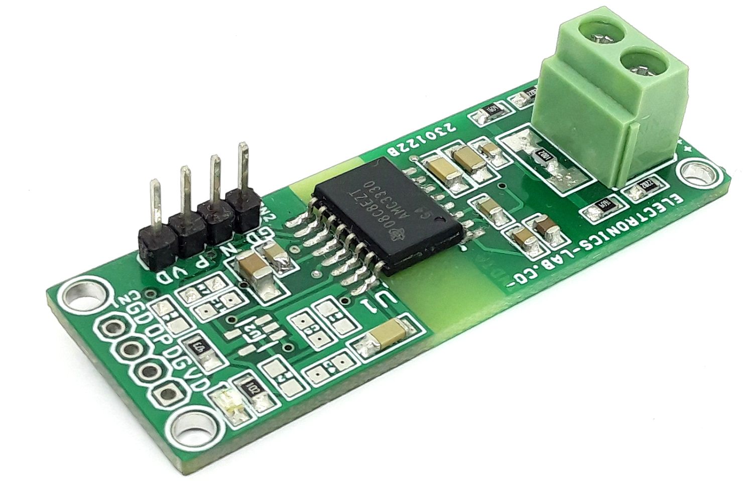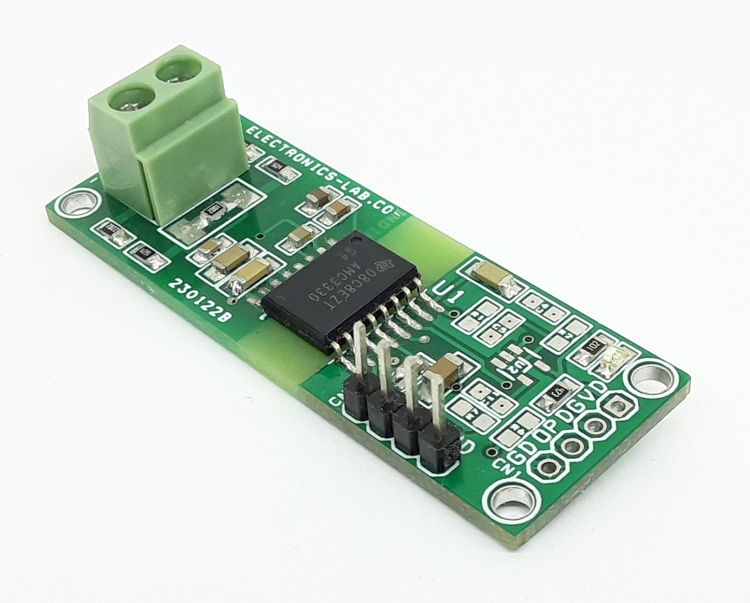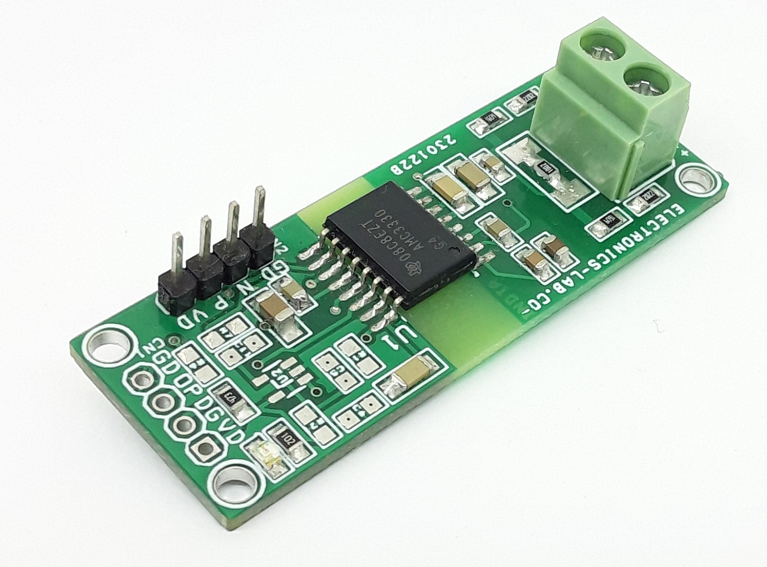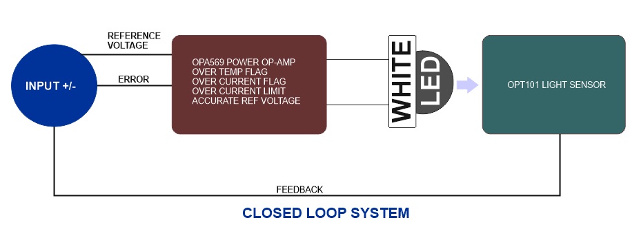
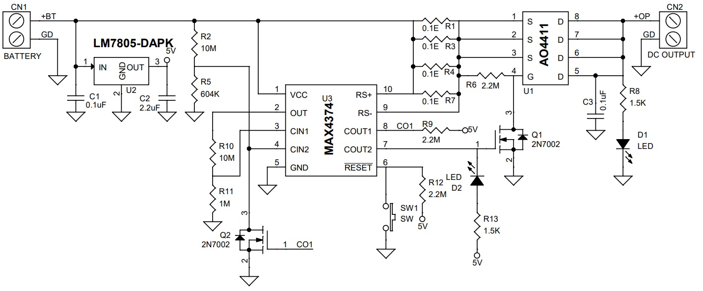
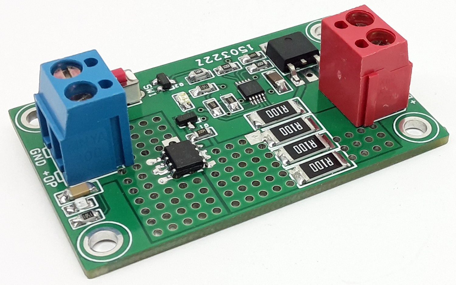
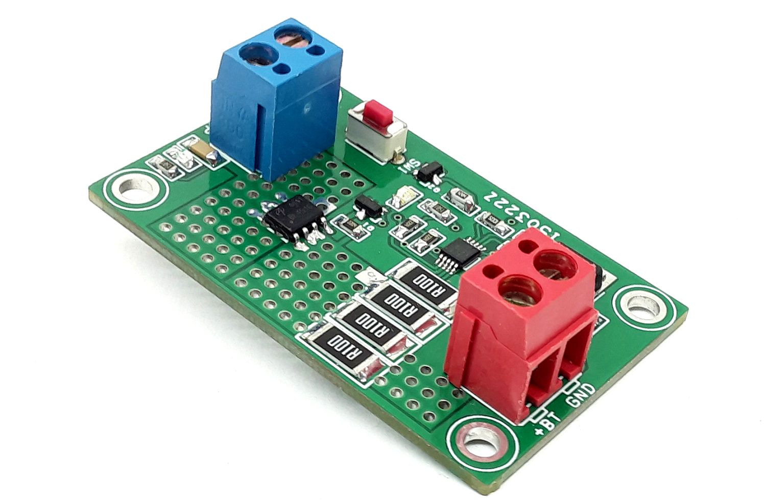
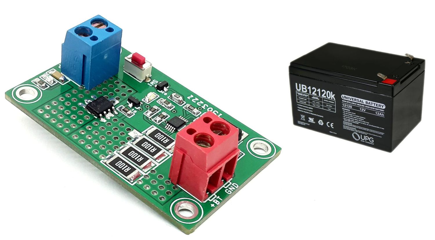
The project described here protects and monitors a Lead-Acid battery against too-low battery voltage and over-current conditions. The circuit consists of MAX4373 current-sense amplifier with internal dual comparators and P-channel MOSFET in series with the battery and its load. It works as a normally closed switch which can be opened if the current-sense amplifier and comparators detect either a high load current OR a low battery voltage. When over current condition occurs, the comparator latches the output and can be reset by onboard push switch SW1.
The circuit protects a lead-acid battery by disconnecting its load in the presence of excessive current (more than 5A), or a low terminal voltage indicating excessive discharge (< 10.5V). The battery and load are connected using 0.025Ω current-sense resistors (R1, R3, R4, R7) and P-channel power MOSFET U1. U1 can handle 30V of drain-source voltage and continuous current greater than 5A.
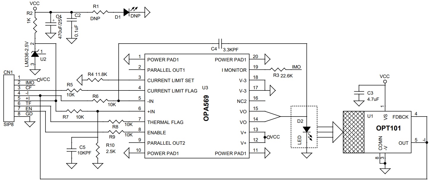
IC U3 is a micropower device drawing only 50µA of supply current. It contains a dual comparator and a high-side current-sense amplifier whose output current is proportional to the current through (R1+R3+R4+R7). The top comparator (C2) senses battery voltage via R2/R5, and drives COUT2 low when the voltage falls below 10.5V. That action turns on LED D2, turns off Q1, and allows R6 to turn off U1 by pulling its gate high. Thus, the battery load is removed when the battery voltage is less than 10.5V. Recharging the battery turns U1 back on automatically. C2’s internal 1.5% hysteresis prevents output oscillation near the switching threshold. A linear regulator U2 provides a stable 5V for pull-up resistors R9 and R12. It also sources the 2.5mA required for fault indicator LED D2. LED D1 indicates the output power.
The output of latched comparator C1 is normally low, which turns off Q2 and allows normal operation. When a load current above 5A drives the CIN1, the voltage goes above 0.6V, the open-drain output COUT1 is latched high (open), allowing R9 to pull T2’s gate high. The resulting low on CIN2 drives COUT2 low, disconnecting the load and illuminating LED D2 just as an over-discharge does, except the load remains disconnected until U3’s active-low RESET input (normally pulled high via R12) is pulled to ground via the normally-open pushbutton switch SW1.
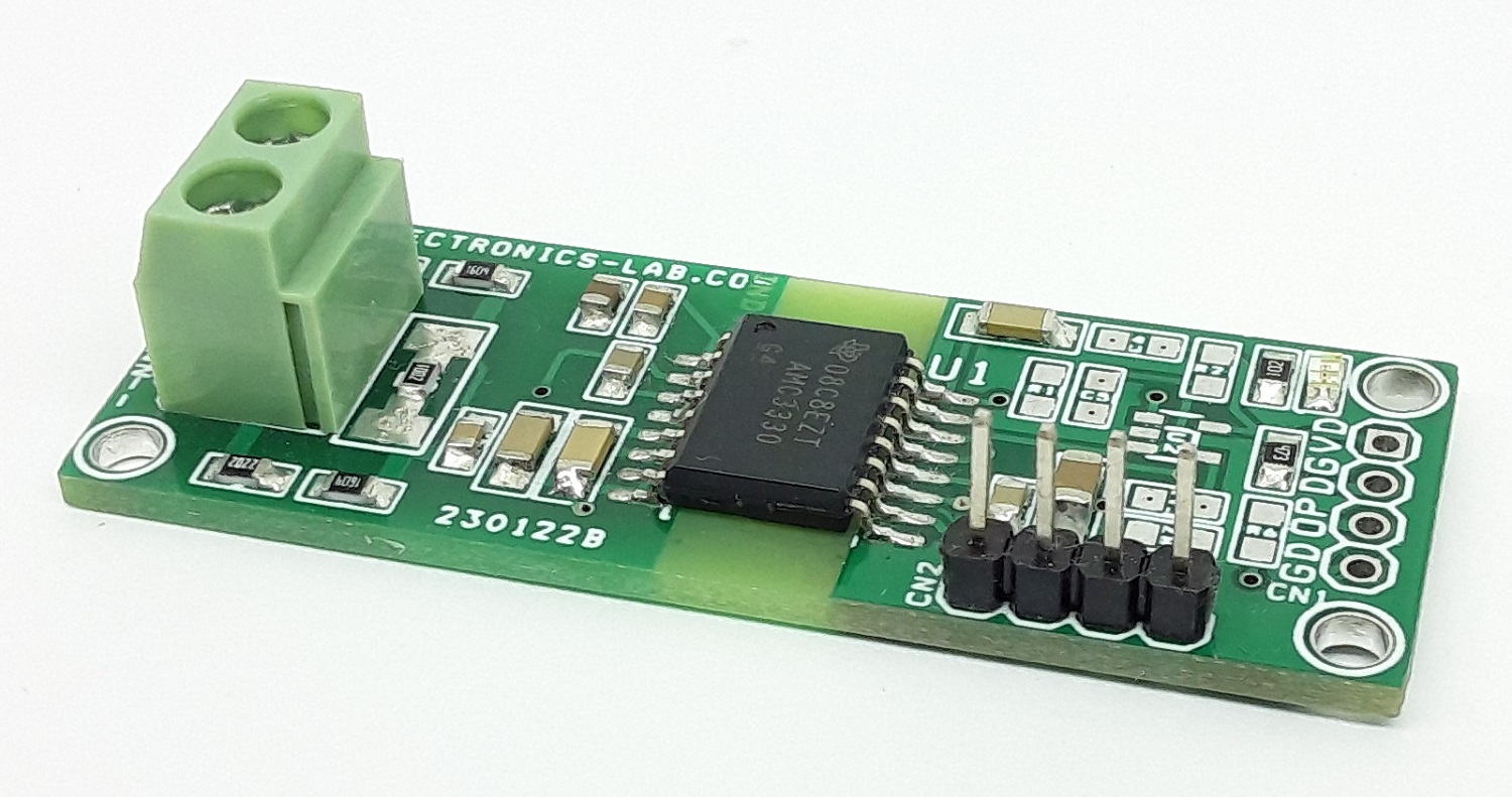
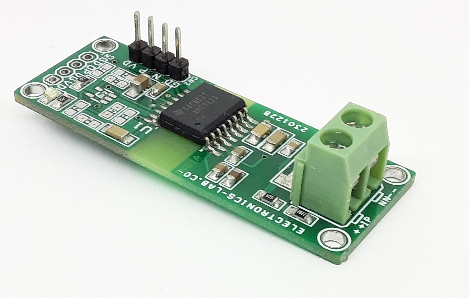
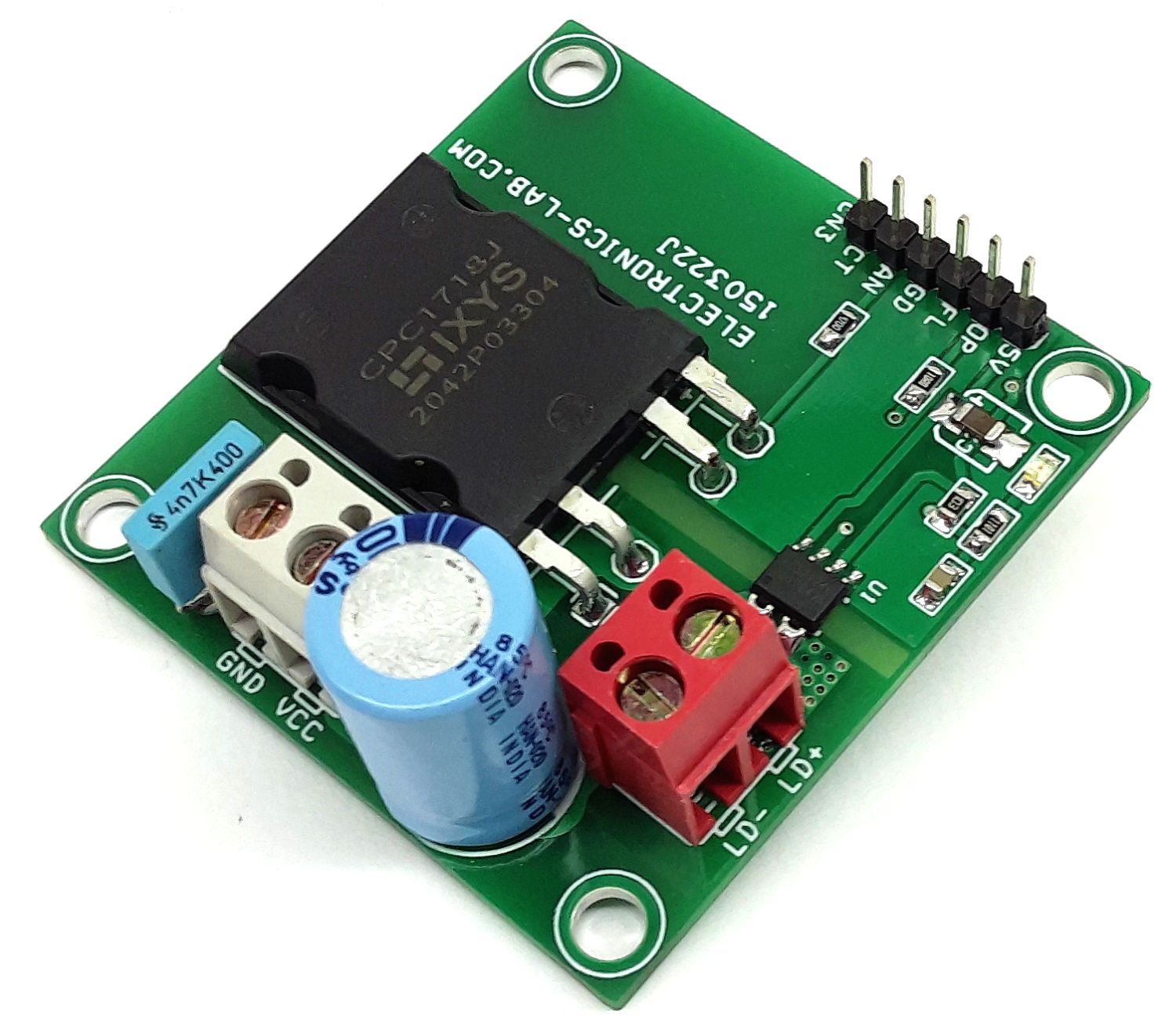
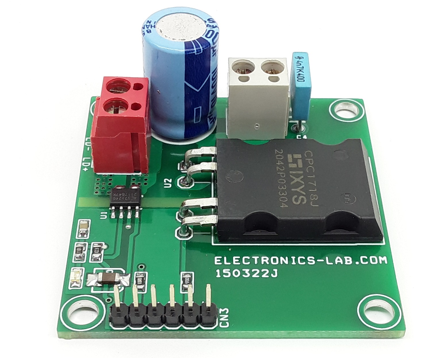
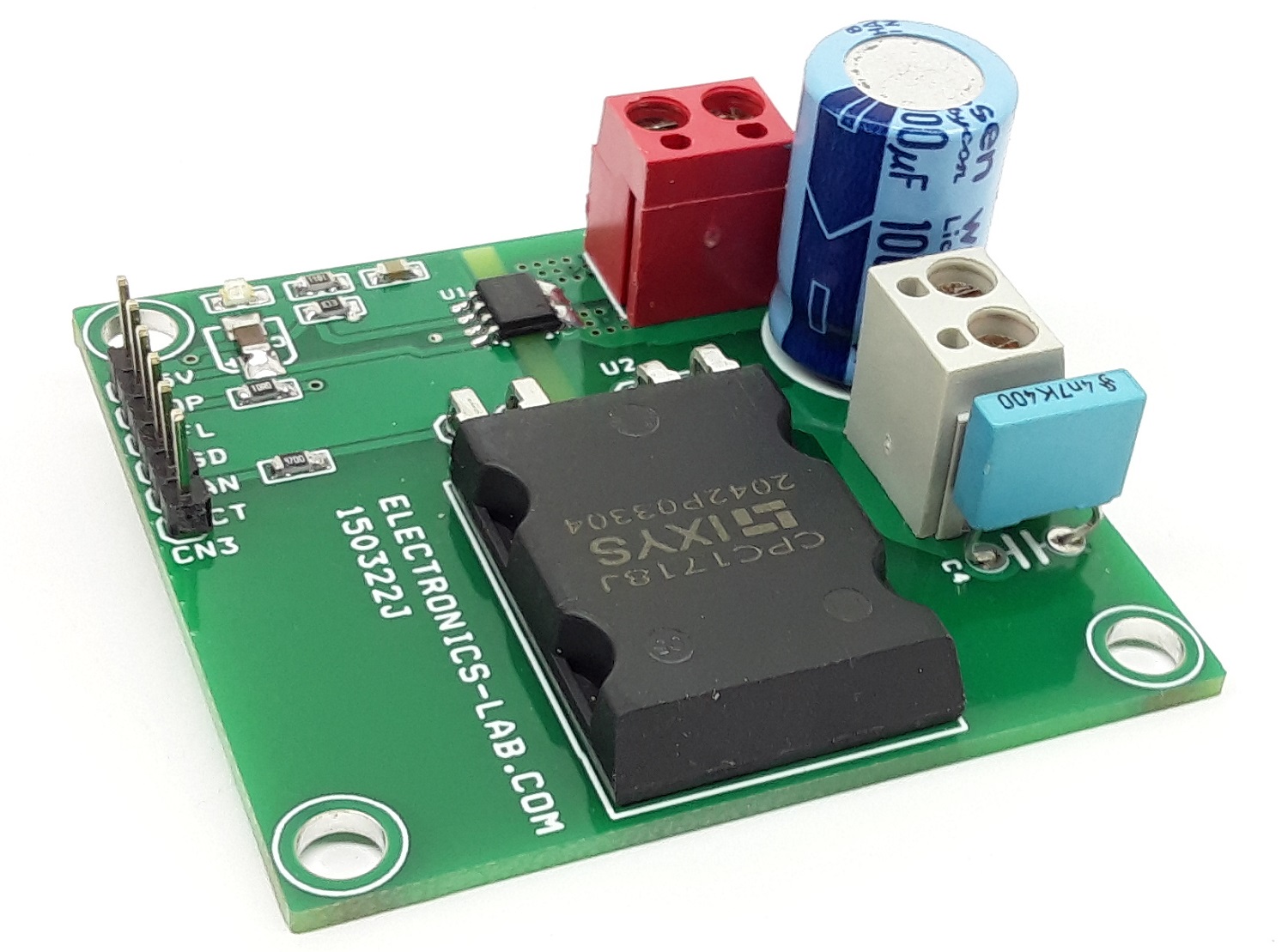
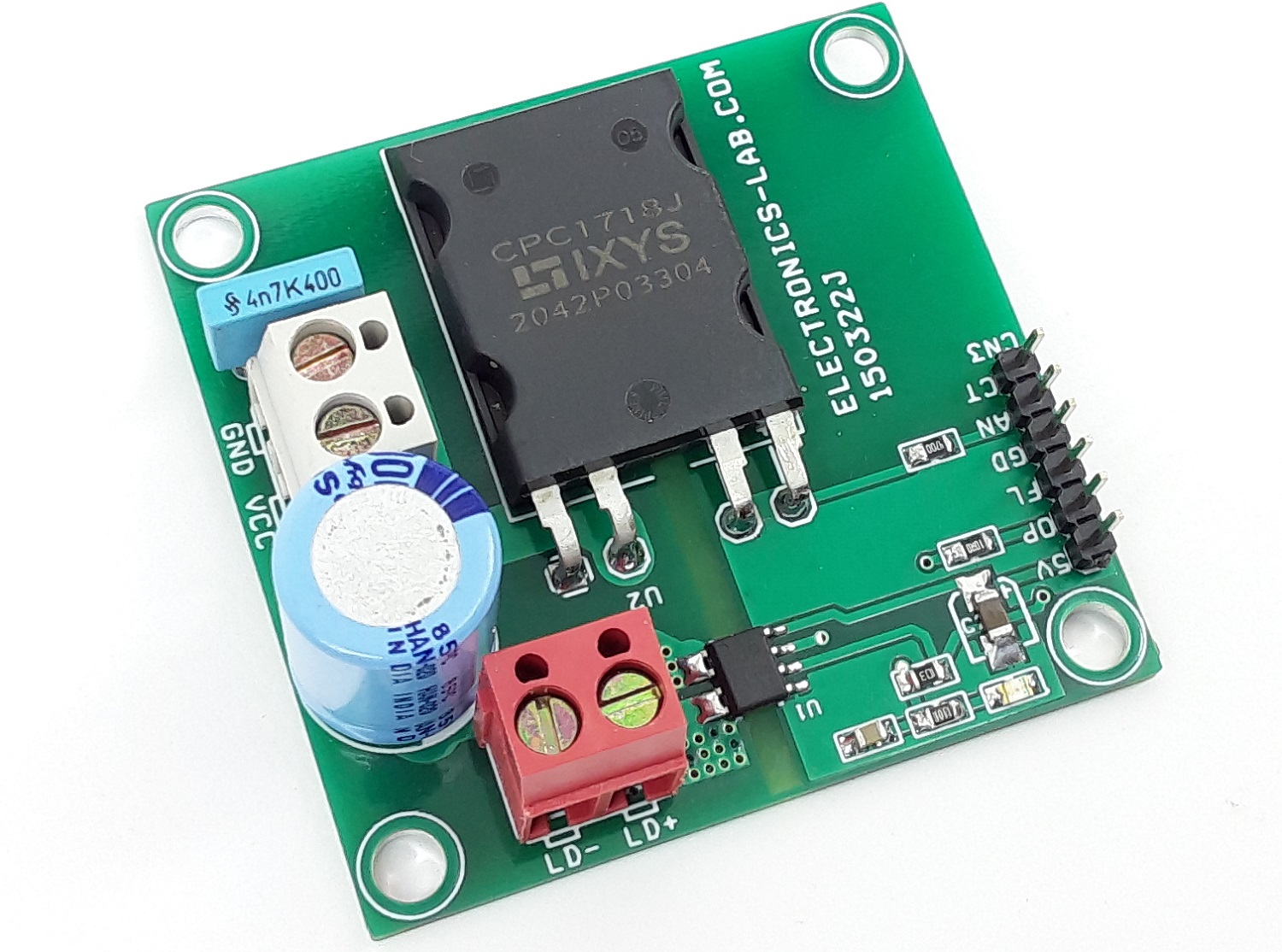
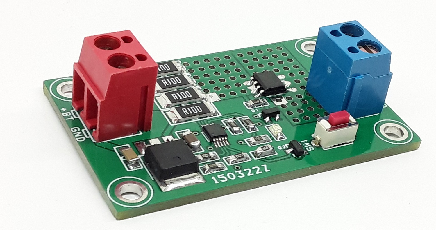
Connections and Other Details
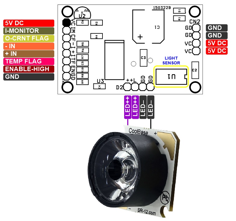
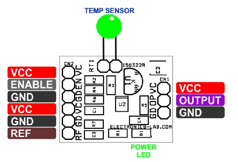
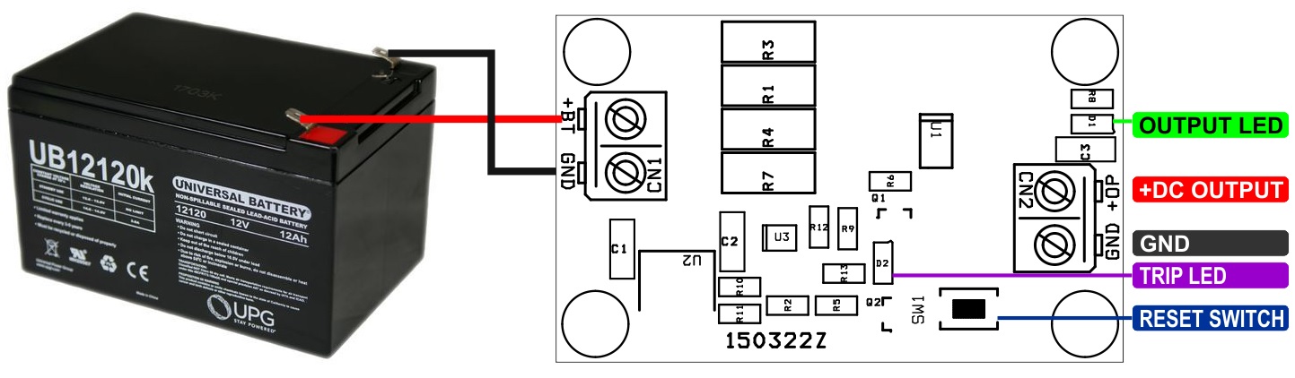
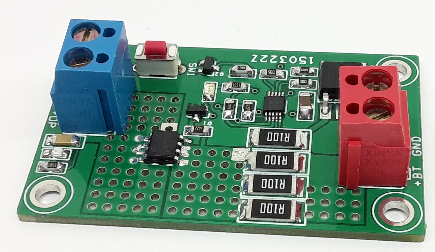
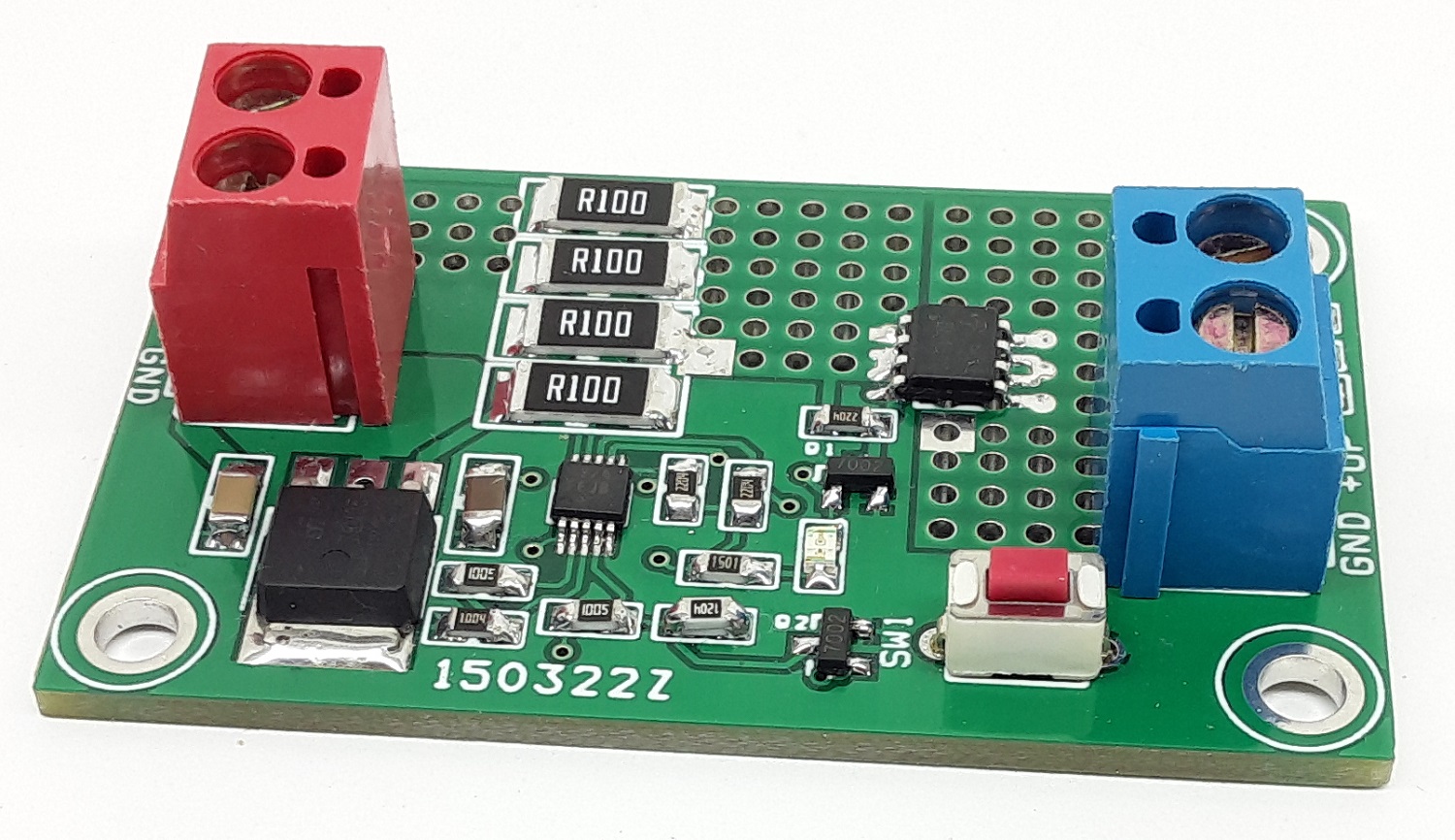
- CN1: Pin 1 Battery Red Terminal +12V, Pin 2 Battery Black Terminal GND
- CN2: Pin 1 + DC Output, Pin 2 GND
- D1: Output Power LED
- D2: Fault LED Over Voltage OR Over Current
- SW1: Reset Switch
Features
- Input 12V Lead Acid Battery
- Output Load Current up to 5A
- Low Battery Threshold 10.5V
- On Board Reset Switch
- On-Board Fault LED
- On-Board Output LED
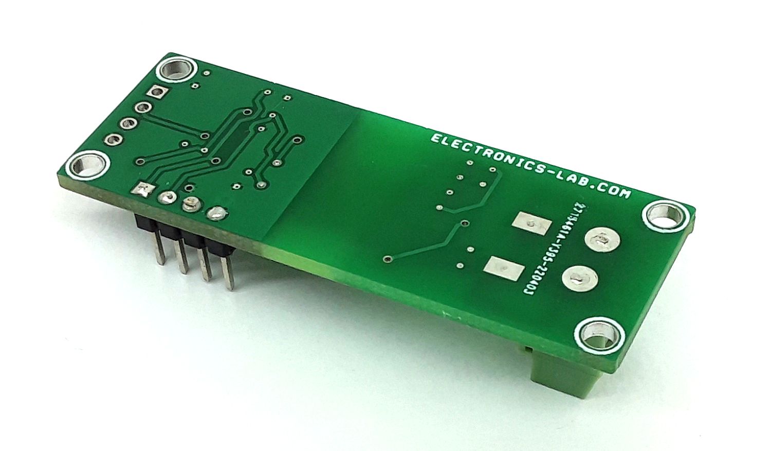
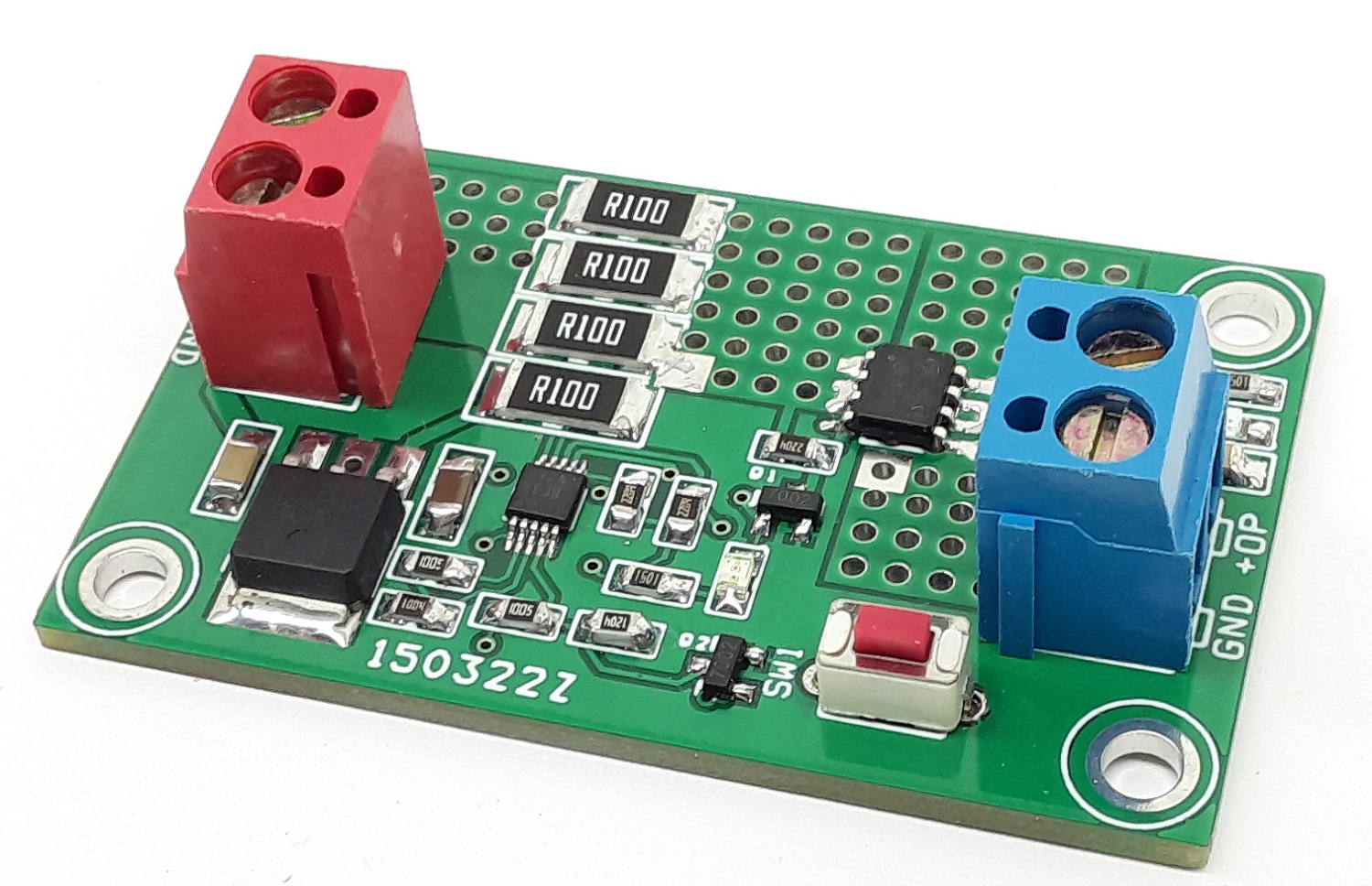
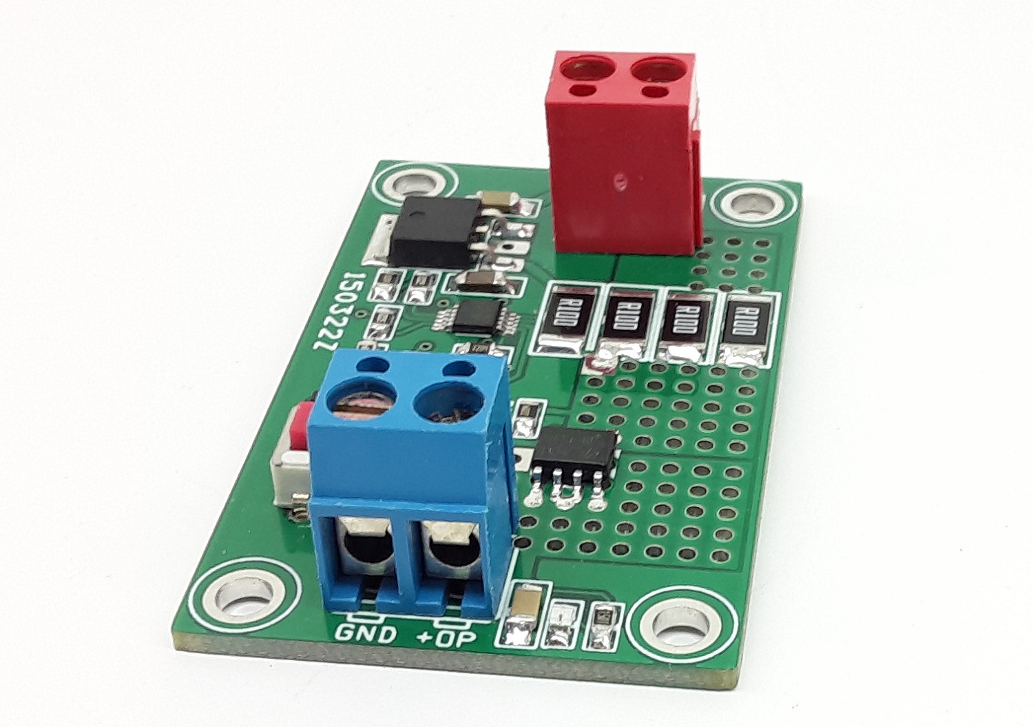
- PCB Dimensions 53.18 x 32.86mm
- 4 x 3mm Mounting Holes
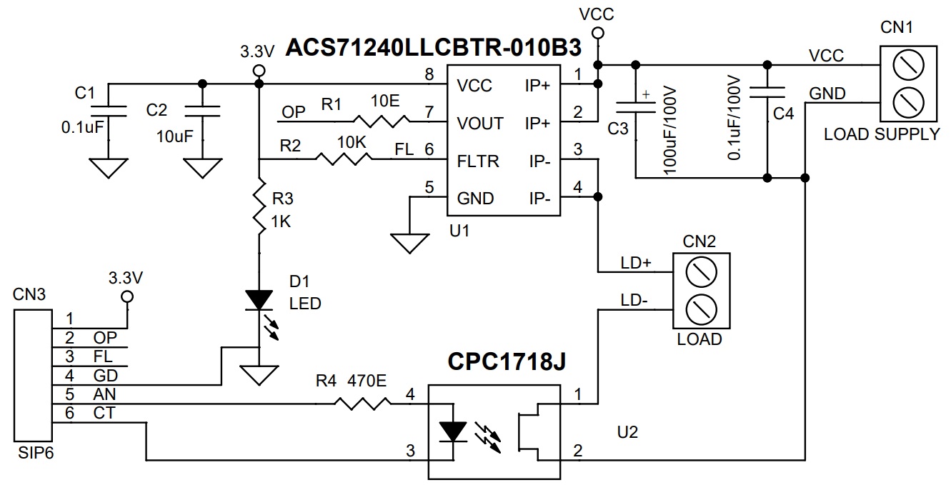
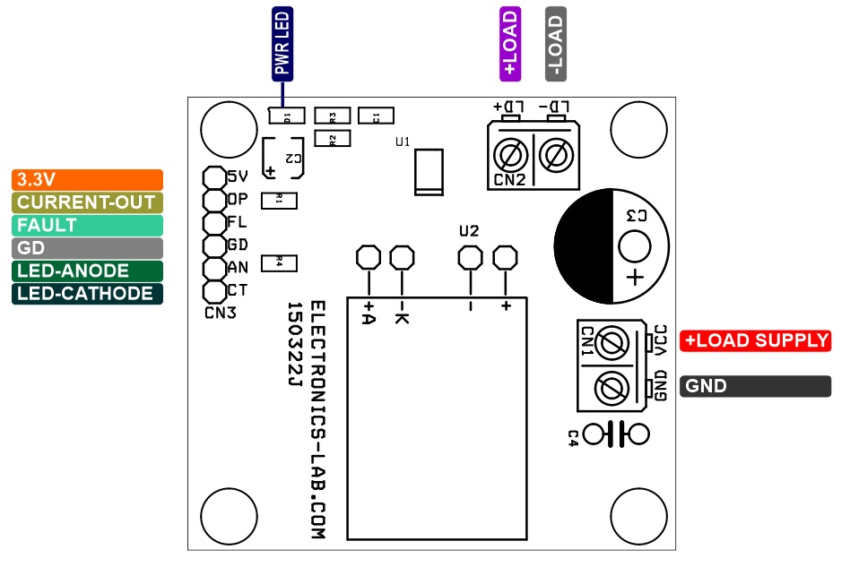
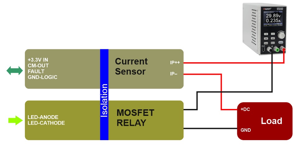
Schematic
Parts List
| NO | QNTY | REF. | DESC. | MANUFACTURER | SUPPLIER | PART NO |
|---|---|---|---|---|---|---|
| 1 | 1 | CN1 | 2 PIN SCREW TERMINAL PITCH 5.08MM | PHOENIX | 277-1247-ND | |
| 2 | 1 | CN2 | 2 PIN SCREW TERMINAL PITCH 5.08MM | PHOENIX | 277-1247-ND | |
| 3 | 2 | C1,C3 | 0.1uF/50V CERAMIC SMD SIZE 1206 | YAGEO/MURATA | ||
| 4 | 1 | C2 | 2.2uF OR 10uF/25V SMD SIZE 1206 | YAGEO/MURATA | ||
| 5 | 2 | D1,D2 | LED RED/GREEN SMD SIZE 0805 | LITE ON INC | 160-1427-1-ND | |
| 6 | 2 | Q1,Q2 | 2N7002 SOT23-3 | DIODE INC | 2N7002-FDITR-ND | |
| 7 | 4 | R1,R3,R4,R7 | 0.1E/1W 1% SMD SIZE 2512 | YAGEO/MURATA | ||
| 8 | 2 | R2,R10 | 10M 1% SMD SIZE 0805 | YAGEO/MURATA | ||
| 9 | 1 | R5 | 604K 1% SMD SIZE 0805 | YAGEO/MURATA | ||
| 10 | 3 | R6,R9,R12 | 2.2M 1% SMD SIZE 0805 | YAGEO/MURATA | ||
| 11 | 2 | R8,R13 | 1.5K 5% SMD SIZE 0805 | YAGEO/MURATA | ||
| 12 | 1 | R11 | 1M 1% SMD SIZE 0805 | YAGEO/MURATA | ||
| 13 | 1 | SW1 | TACTILE SWITCH 2 PIN | E-SWITCH | EG2513-ND | |
| 14 | 1 | U1 | AO4411 P CHNL MOSFET SOIC8 | ALPHA & OMEGA | 785-1284-1-ND | |
| 15 | 1 | U2 | LM7805-DAPK | TI | LM78M05CDTX/NOPBTR-ND | |
| 16 | 1 | U3 | MAX4374 | ANALOG DEVICE | MAX4374HEUB+-ND |
Connections
Gerber View
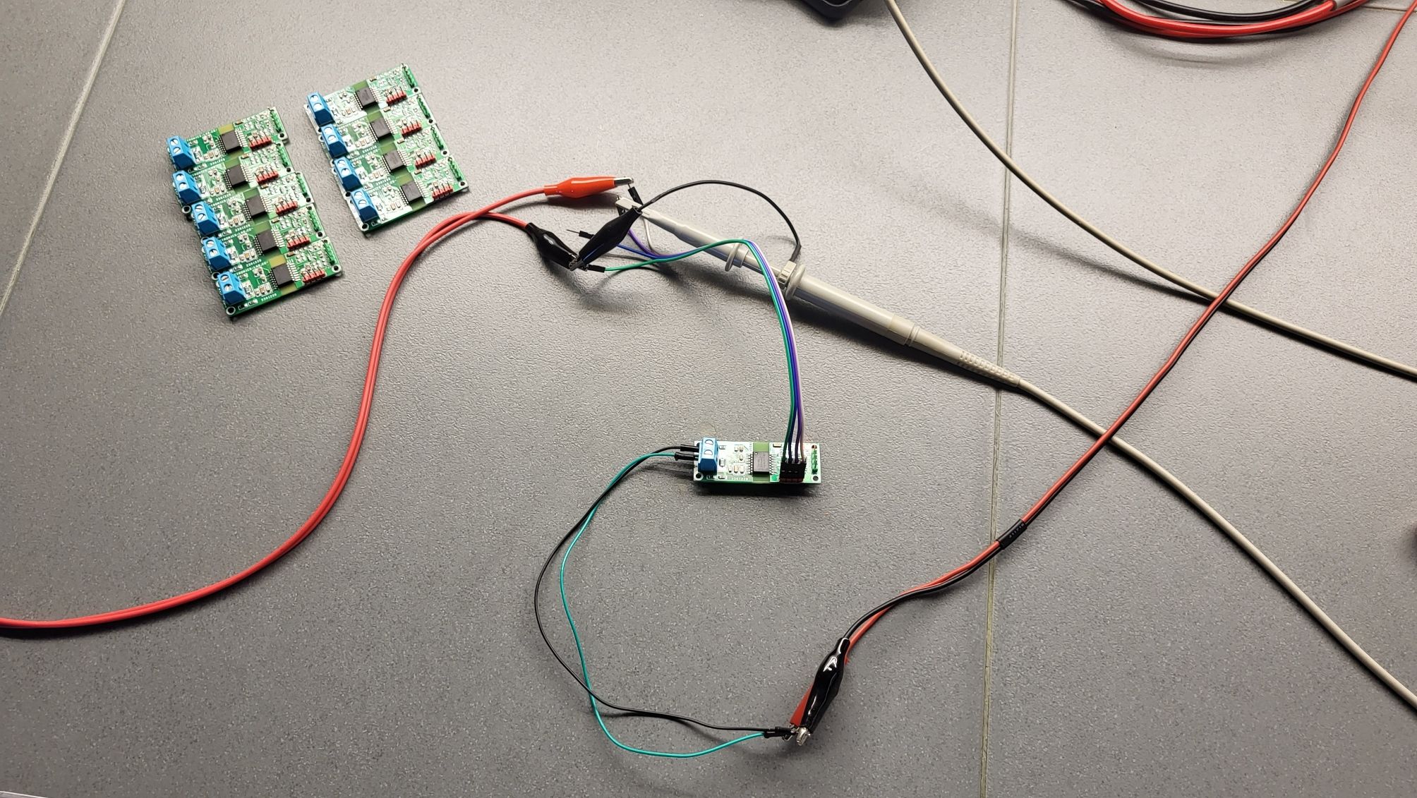
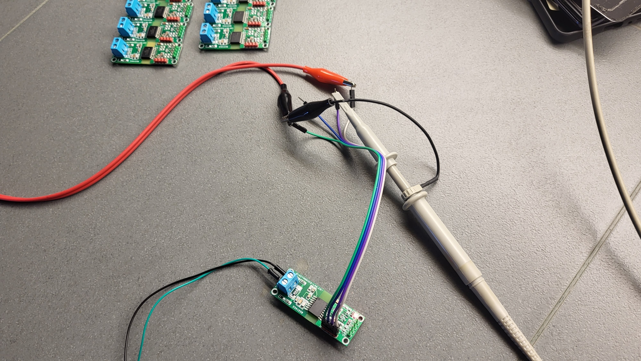
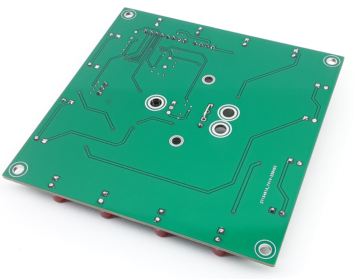
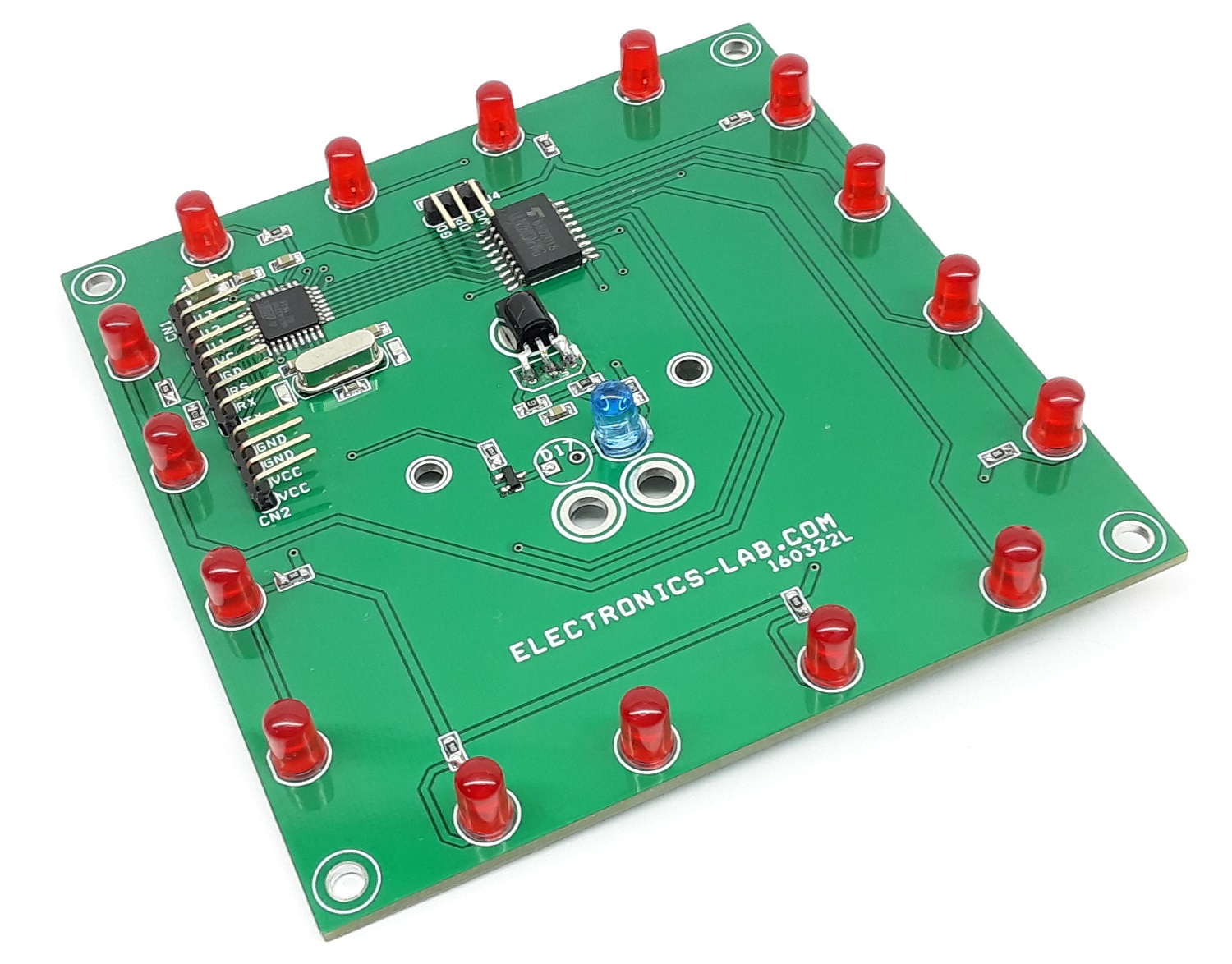
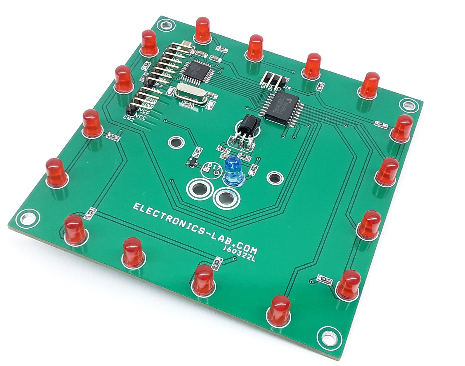
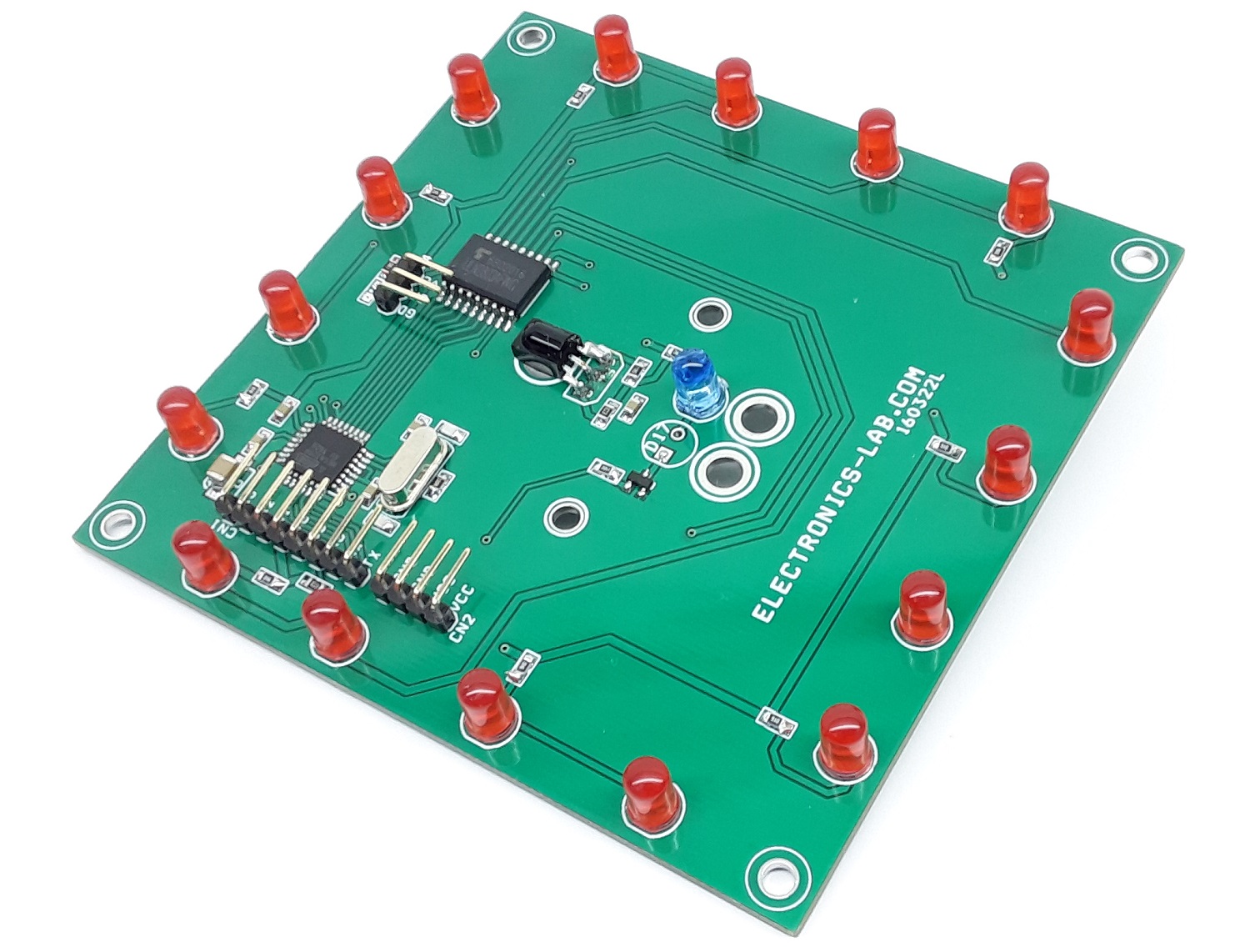
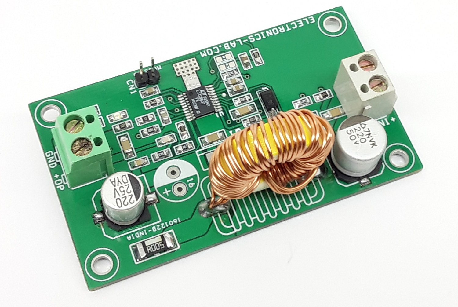
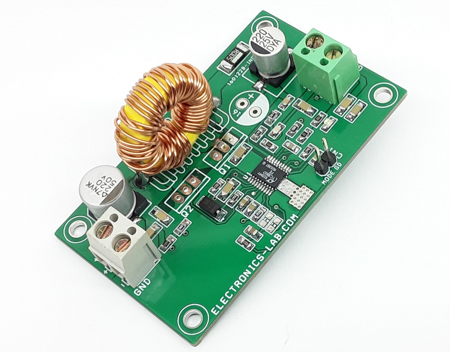
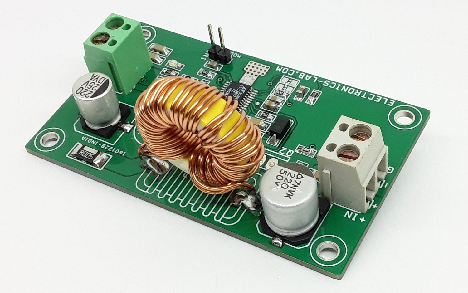
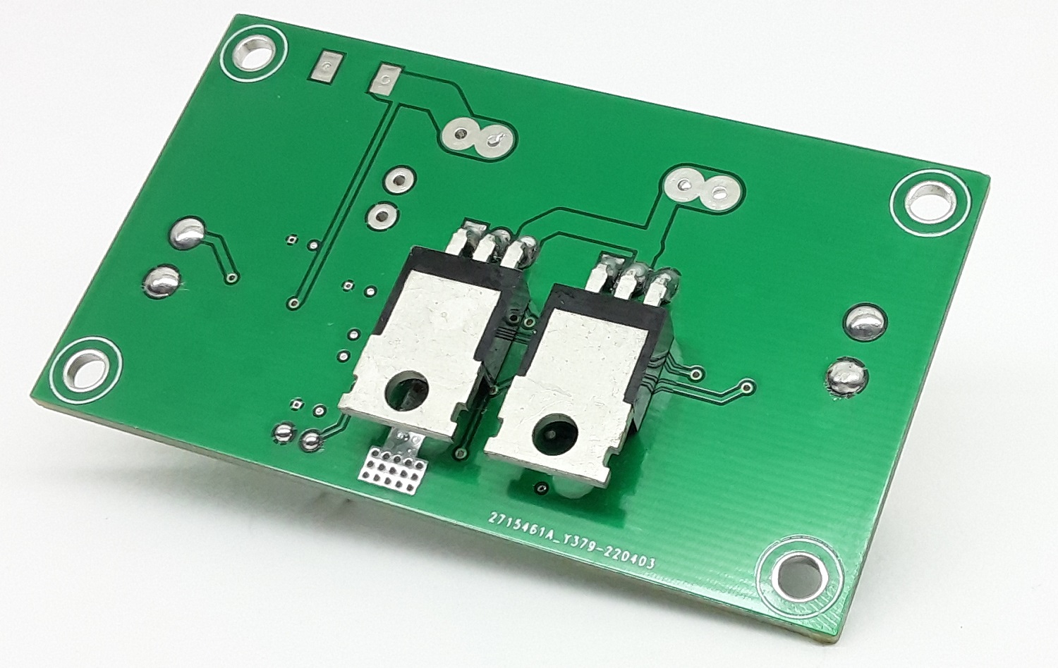
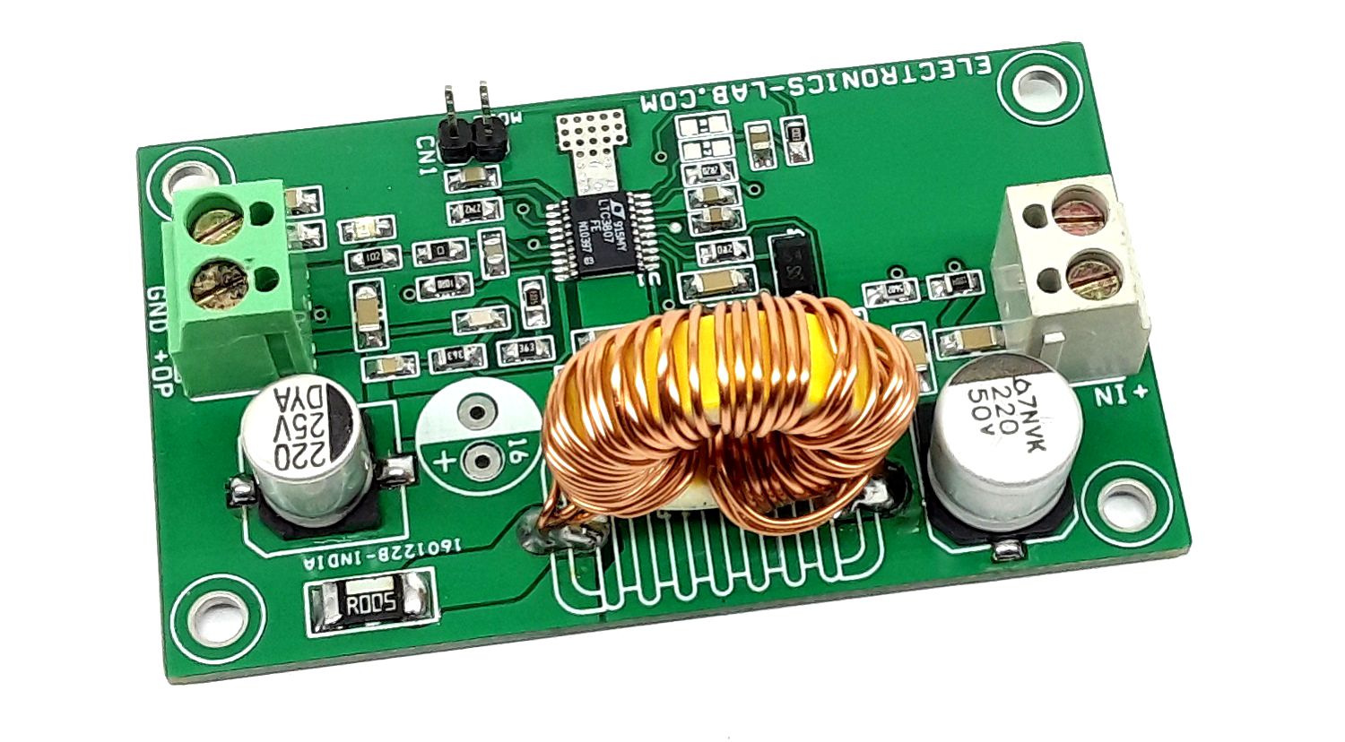
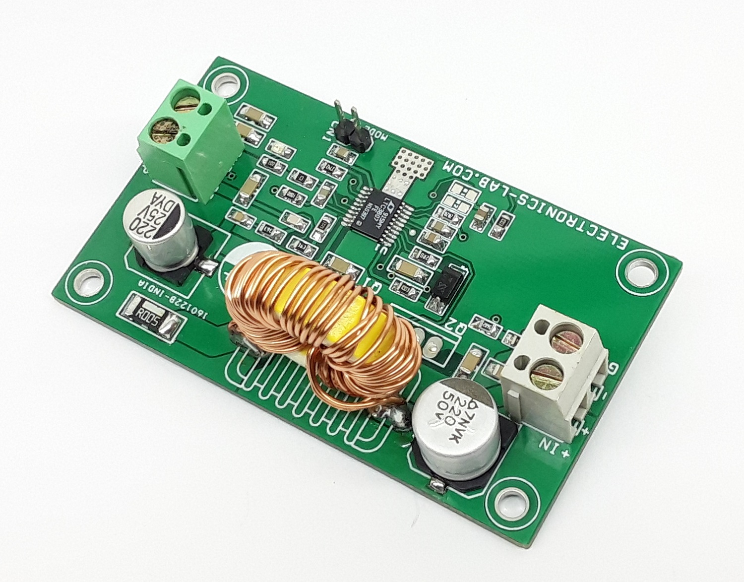
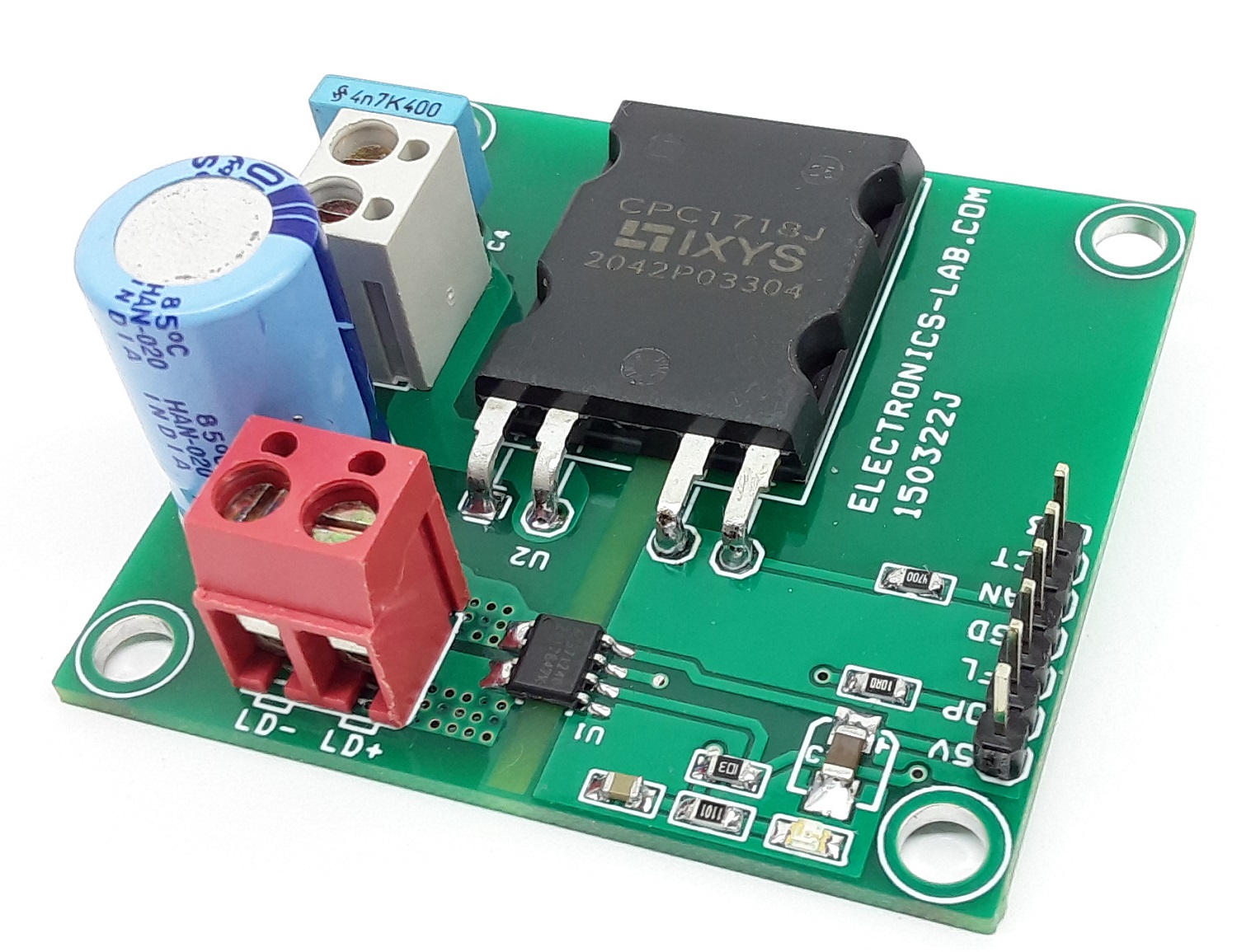
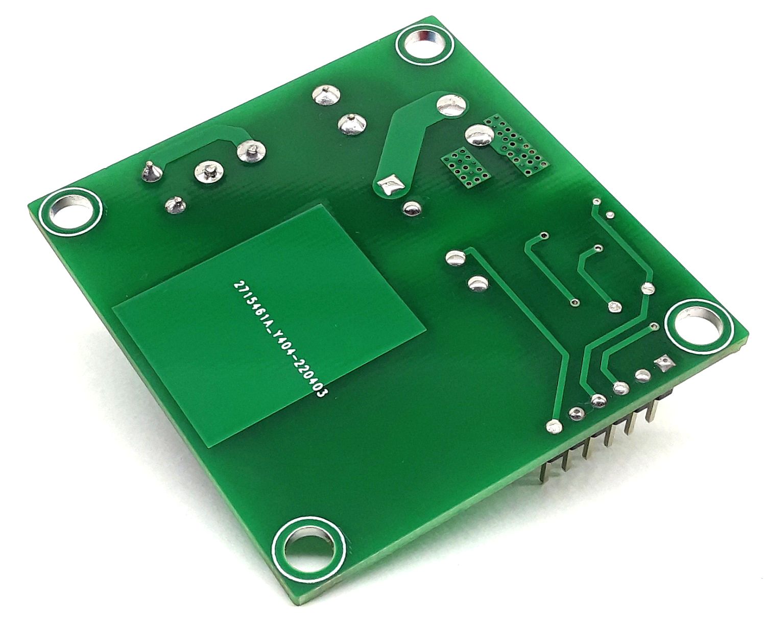
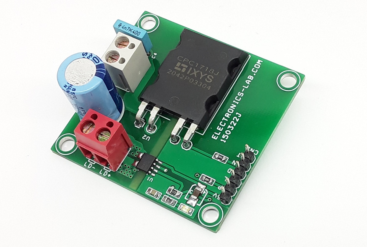
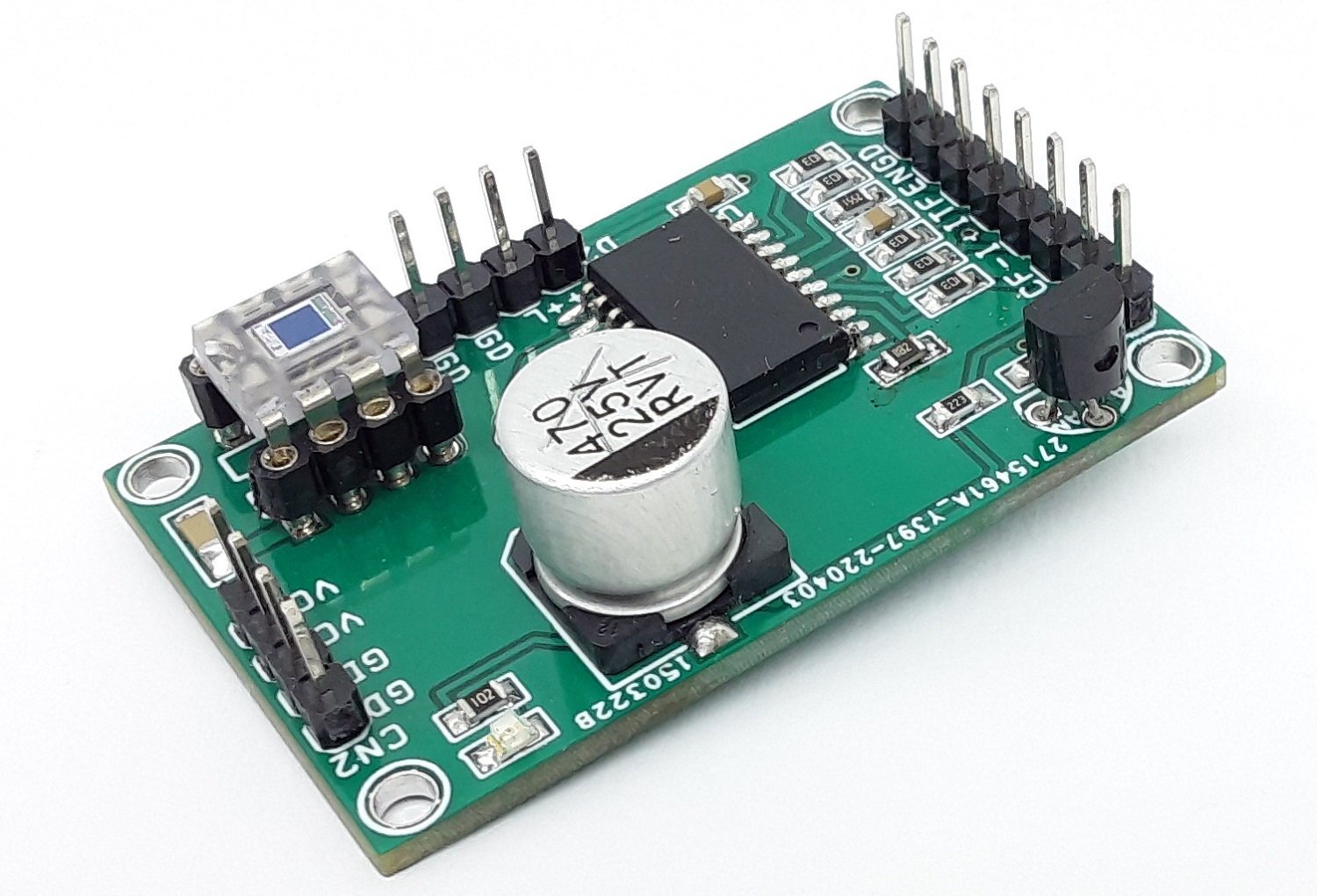
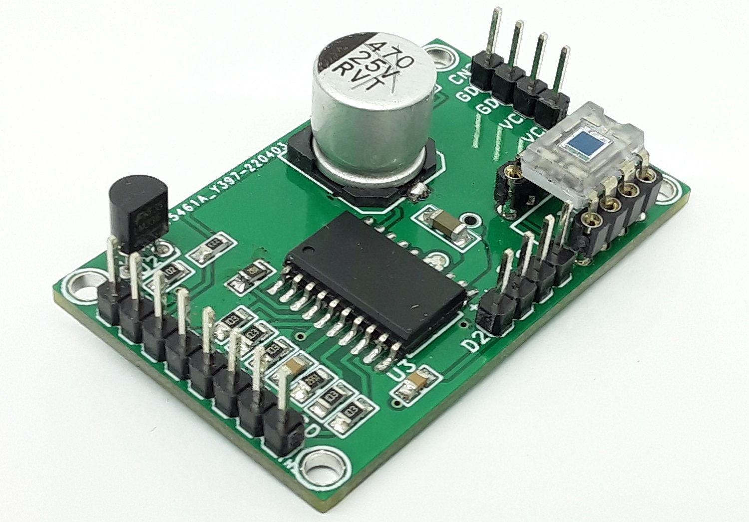
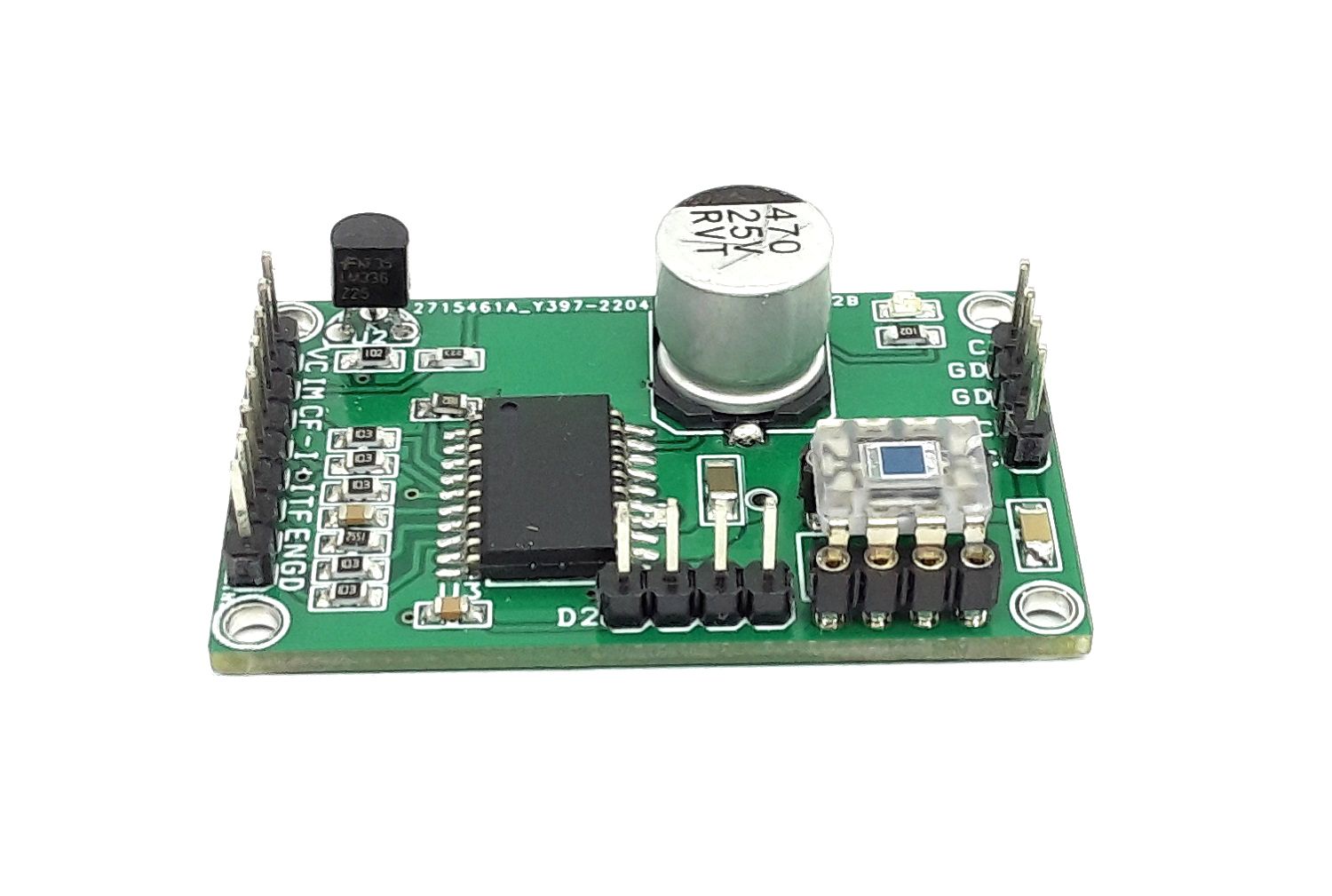
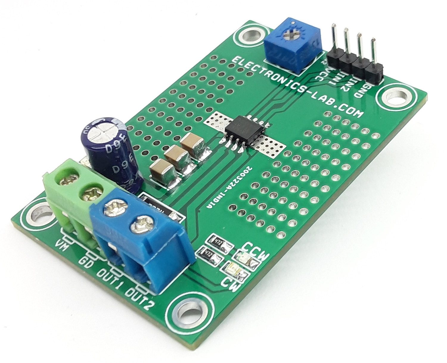
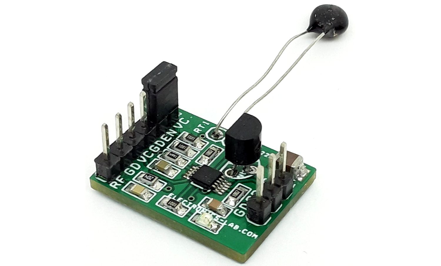
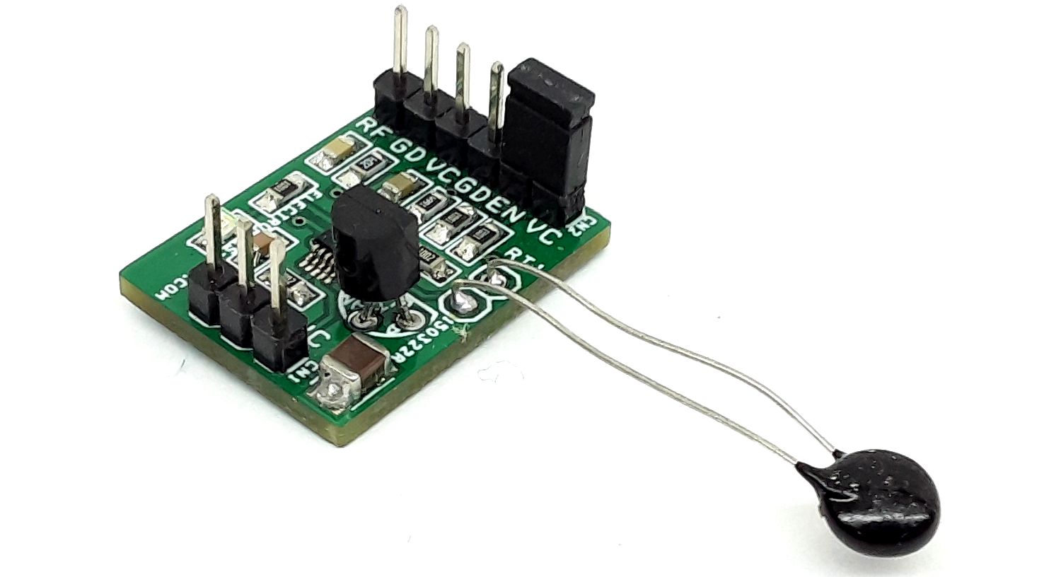
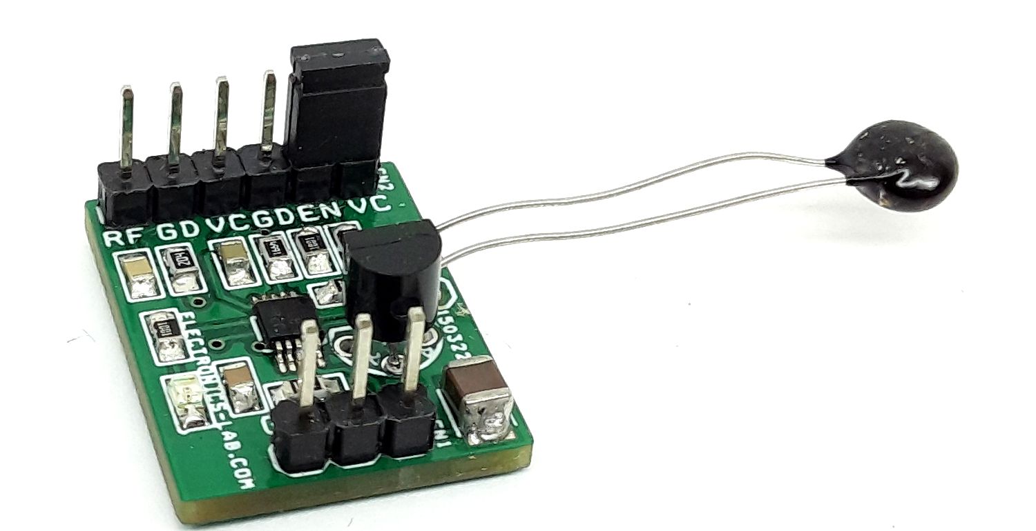
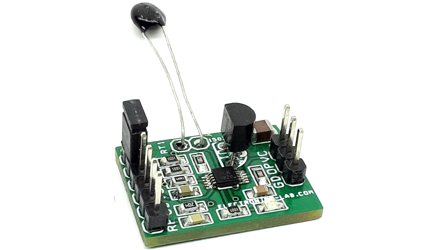
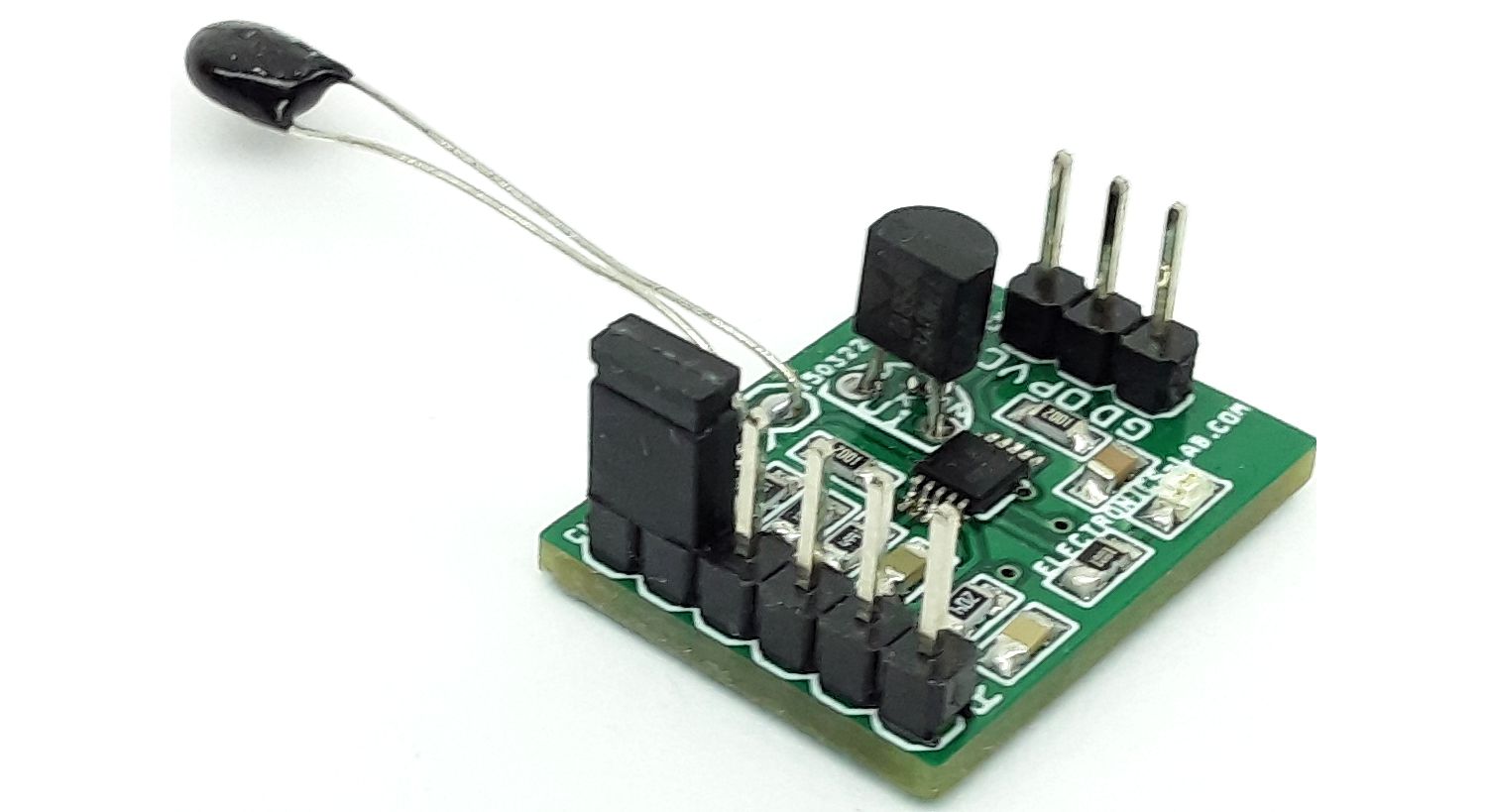
Photos
Video