Many people seem to be talking a lot about edge computing these days but the fact remains that the word still means different things to different people having different needs within the edge computing space. It happens most times that some applications even require additional optimizations out of their hardware, maybe a bit of extra focus on its connectivity, its power, or its performance, which makes edge computing platforms look architecturally different from one another.
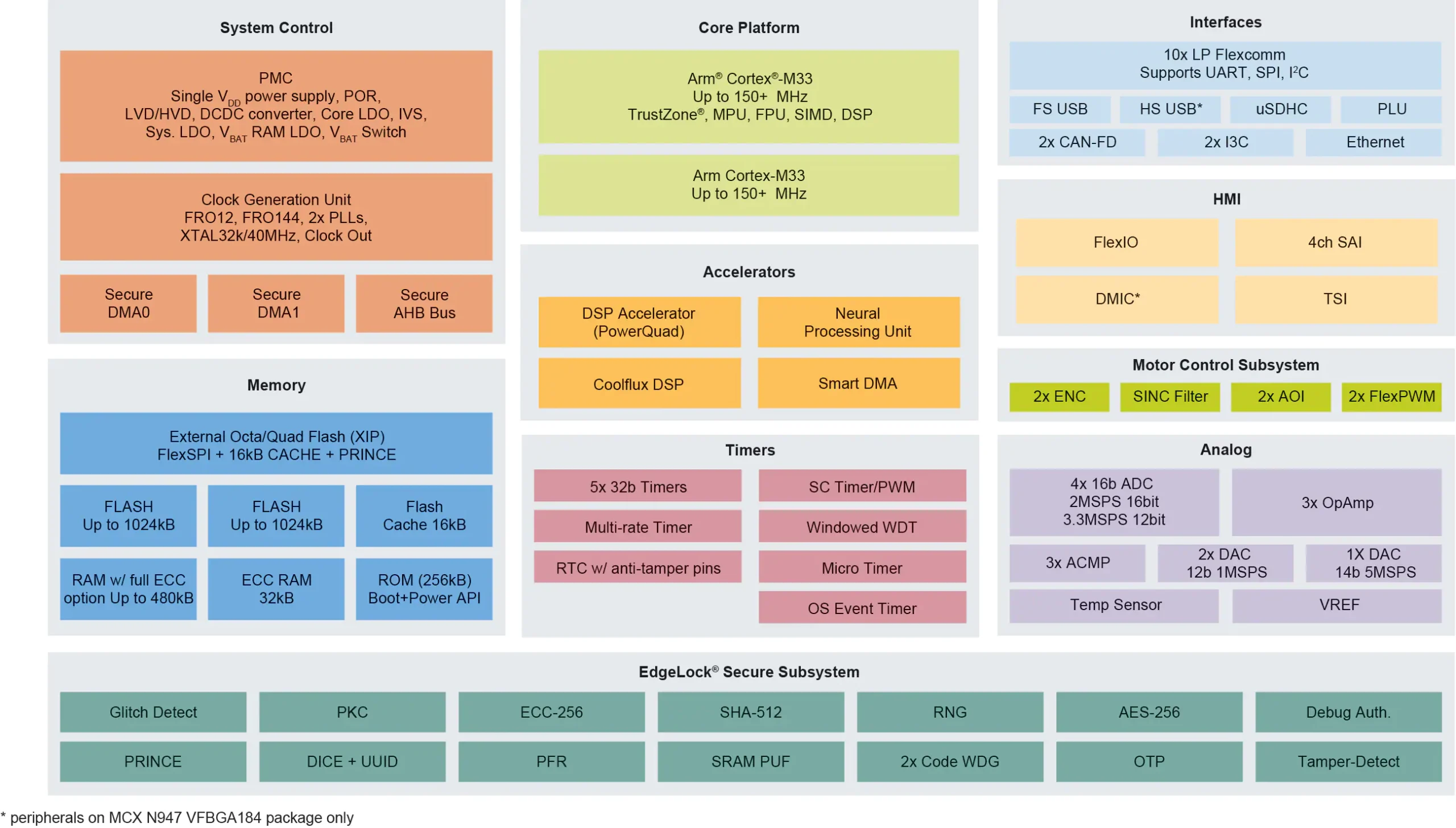
To address some challenges that this diversity often creates for designers, NXP Semiconductors has announced its intentions to launch a family of 4 new MCUs that target different needs within the edge computing space — something for everyone designing for Edge AI. One of these is the MCX N Advanced microcontrollers designed for high-performance energy-efficient edge AI workloads.
“Developers are increasingly looking to push the boundaries of what’s possible at the edge as they create new devices that can better anticipate and automate in smart homes, smart factories, and smart cities. This requires advanced MCUs [Microcontroller Units] that are more efficient, simplify edge intelligence, and do all of that securely,” NXP’s Rafael Sotomayor explains. “As we look to the future of MCUs, the MCX N series delivers the balance between power and performance for tomorrow’s IoT and industrial applications.”
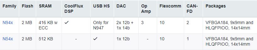
The MCX N series designed for secure and intelligent applications promises low power consumption and a significant performance boost to edge AI performance. The series is offered in two models namely the MCX N94x and MCX N54x, both of which use a heterogeneous multi-core design with an Arm Cortex-M33 core and a streamlined core designed for control functions. The company also introduced an in-house neural processing unit architecture into the mix, which they claim to offer a third-fold performance gain for machine learning workloads.
“The multicore design delivers improved system performance and reduced power consumption by enabling smart, efficient distribution of workloads to the analog and digital peripherals,” says NXP’s CK Phua. “As a result, the MCUs consume less than 45μA/MHz active current, less than 2.5μA in power-down mode with the real-time clock (RTC) enabled and 8kB SRAM retention, and less than 1μA in deep power-down mode with the RTC active and 8kB SRAM.”
The two models offer equivalent performance but while the N94x chips offer peripherals designed for analog and motor control workloads, the N54x chips focus on high-speed USB with PHY, SD card, and smart card interfaces for IoT. Both however feature 2MB of flash and 512 kB of SRAM as well as a broad range of peripherals such as an integrated Digital Signal Processor, an EdgeLock secure subsystem, hardware root-of-trust, secure boot, and cryptographic acceleration.
The new MCUs should support the MCUXpresso software suite as well as the company’s development environment for machine learning projects. There would also be a number of RTOS (Real Time Operating System) to choose from.
The new MCUs are due to sample early next year and no particular date has been picked for general availability yet. Other useful details can be found on their website.
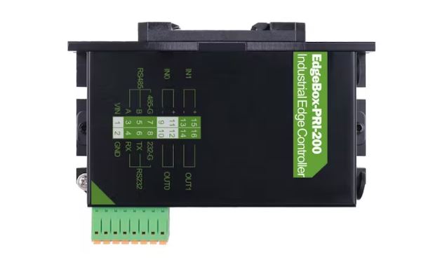
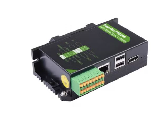
We recently found out that Seeed Studio is offering a set of rugged industrial edge computing controllers designed for a variety of industrial applications: the EdgeBox RPI-200 series.
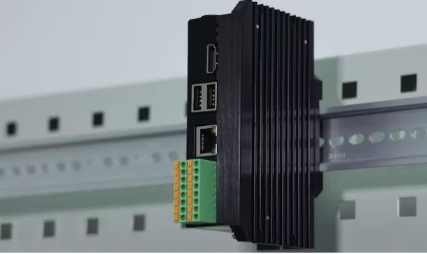
EdgeBox RPI-200 is a complete industrial controller equipped with a flexible and powerful processor capable of performing real-time operation and multi-process. It is powered by AI-enabled Raspberry Pi Compute Module 4 running at up to 1.5GHz and equipped with up to 4GB of RAM and 16GB eMMC.
The system also features rich IO resources and multiple industrial interfaces that achieve data transmission in a variety of situations. It comes with extended SSD storage, an enhanced HDMI 2.0 connection for better visual presentation as well as several communication capabilities such as an RJ45 Gigabit Ethernet and full-featured wireless interconnectivity (built-in 2.4GHz and 5GHz WiFi, Bluetooth 5.0 and Bluetooth Low Energy support). There is also a mini PCIe slot to support the installation of optional 4G cellular LoRaWan Gateway or ZigBee modules. Other features include 2x USB 2.0 ports, one RS485 port, and another RS232 port.
The industrial edge computing controller is small, compact, and lightweight. It is fitted in a rugged and maintenance-reducing high-grade structure with a full aluminum heatsink enclosure for maximum thermal management. It also supports 35mm DIN and wall mount which make it convenient to use where space is limited or in extreme conditions.
The EdgeBox also has great support for a variety of industrial software and platforms, including Codesys, Node-Red, MQTT, OPC UA, etc. It is perfect for high-end applications such as smart automation and control systems, IoT Gateways, 4G LTE Route, software-defined Programmable Logic Controller (PLC), Industrial controllers, edge computing controllers, etc.
Specifications Include:
Quad-core Raspberry Pi CM4 running at up to 1.5GHz
Up to 4GB RAM
Up to 32GB eMMC
Built-in 2.4GHz/5GHz IEEE 802.11 b/g/n/ac WiFi
Bluetooth 5.0, Bluetooth Low Energy (BLE)
1x GbE RJ45 port
Mini PCIe slot support 4G LTE/LoRaWAN Gateway or ZigBee module
1x HDMI 2.0 ports with 4k@60fps
1x M.2 socket support 2242 NVMe SSD
2x USB 2.0 Type-A
2x isolated DI and 2x isolated DO
1x RS-485 and 1x RS-232
1x Real Time Clock (RTC)
1x Watchdog Timer
1x optional UPS unit (Uninterrupted Power Supply)
Support for AWS and Azure Cloud Services
Power Supply: DC 12V to 36V
Dimension: 124 mm x 76 mm x 35 mm
Operating Temperature: -20°C to +60°C
OS: Debian Linux
Certification: RoHS, CE, FCC, TELEC, UKCA
The EdgeBox RPI-200 series is a family of 4 modules. The lowest version comes with 1GB RAM and 8GB eMMC storage and it is the only one without WiFi or Bluetooth. Next to that is the variant with 2GB RAM and 8GB eMMC, while the one ahead of it comes with 4GB RAM and 16GB eMMC. The top variant then comes with 4GB RAM and up to 32GB eMMC memory. All four models cost $229, $239, $269, and $279 respectively.
You can visit the Seeed Studio’s store for more details including purchase links and the corresponding shipping costs.
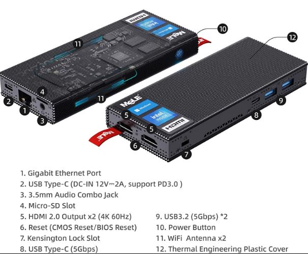
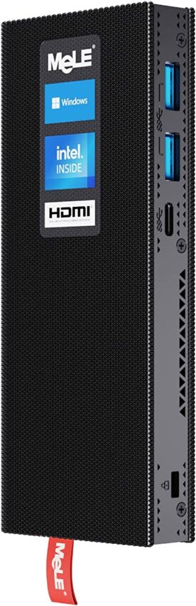
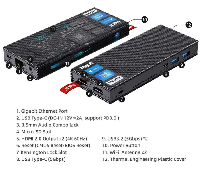
The past few years have seen MeLe expand its PCG02 line of PC Stick, going from the MeLe PCG02 which first launched with an Ethernet port, to the orange stick preloaded with Ubuntu and to several other models which were based on new Intel processors with Apollo Lake and Gemini Lake variants. The company has now introduced a new “Pro” model that is the first in the series to come with support for an optional M.2 2280 PCIe NVMe SSD and the absence of an HDMI male port.
MeLe PCG02 Pro is one desktop PC that you can take with you anywhere you go. It weighs just 182 grams and measures 146 by 61 by 20 mm; as big as an iPhone 14 Pro but small enough to easily slide into your pocket without any struggles.
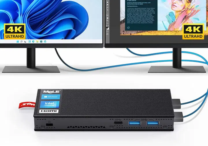
The fanless computer is offered in two variants which are powered differently by the Celeron J4125 Gemini Lake processor or the Celeron N5105 Jasper Lake Intel processor. It comes with 8GB of LPDDR4 memory and a storage interface that can be configured with 128GB/256GB/512GB of eMMC. The MeLe PCG02 Pro also packs flexible peripherals such as 2x USB 3.2 ports, 1x GbE RJ45 port, and 2x 4K@60Hz HDMI ports which are capable of driving two independent displays. It is further equipped with WiFi 5 or Wifi 6 connectivity as well as Bluetooth 4.2 or Bluetooth 5.2 depending on the particular variant and comes with an M.2 NVMe/SSD Storage in the mini PC stick that is only available in the Gemini Lake model.
The two variants of the computer ship pre-installed with Windows 11 Pro but they should also support most Linux distributions such as Ubuntu and Debian.
Specifications Include:
CPU: Intel Celeron J4125 quad-core Gemini Lake Refresh processor at up to 2.7 GHz (J4125) or Intel Celeron N5105 quad-core Jasper Lake processor at up to 2.9 GHz (N5105)
GPU: Intel UHD 600 graphics at 250/750 MHz (J4125) or Intel UHD 605 graphics at 450/800 MHz (N5105)
8GB LPDDR4 2133MHz / 2933MHz (J4125 / N5105)
128GB to 512GB eMMC flash
1x microSD card reader of up to 2TB
M.2 NVMe or SATA SSD support up to 4TB (J4125 only)
1x Gigabit Ethernet LAN port
WiFi 5 (J4125) and WiFi 6 (N5105)
Bluetooth 4.2 (J4125) and Bluetooth 5.2 (N5105)
2x 4K@60Hz HDMI 2.0 ports
1x 3.5mm earphone jack
Digital audio output via HDMI
1x USB Type-C (5Gbps)
2x USB 3.2 (5Gbps)
CMOS Reset
1x Kensington Lock slot
1x Power button
2x WiFi antenna
Power: 12V/2A via USB Type-C (supports USB PD3.0)
Dimension: 146 mm x 61 mm x 200 mm
Weight: 182 grams
Operating System: Windows 11 Pro
Fanless Tech is selling the Celeron J4125 variant of the Pro PC for around $229 and up while the Celeron N5105 variant, which delivers a higher CPU and graphics performance as well as better wireless capabilities, starts at $249. Please note that the varying prices depending on the size of the eMMC flash storage that they are delivered with.
Amazon also sells all variants of the mini PC but they come with a $30 off coupon for customers in the United States.
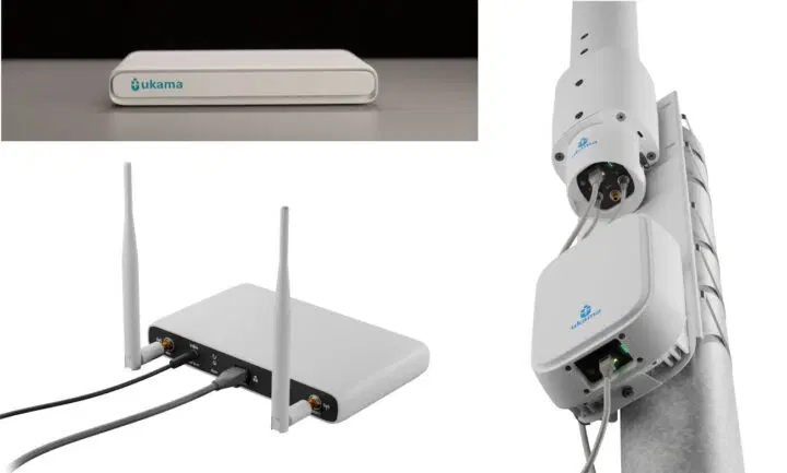
A great team of hardware and software engineers passionate about making life easier for people has provided a way for individuals and enterprises to create a custom 4G LTE-based cellular network with a modern stack. The team designed a decentralized cellular-data network that can be deployed and controlled by anyone anywhere.
“Ukama makes cellular internet accessible to everyone — whether you are looking for free, faster streaming on your smartphone at home, or bringing cellular data connectivity to a rural area for the first time, or rolling out a secure industrial IoT network,” says Kashif C. Ali, CEO and founder of Ukama. “It is a complete solution that includes SIMs (and support for eSIMs), a cellular base station, distributed and embedded cellular Core, a management console, and cloud services.”
Ukama is very easy to use and set up. All you need is electrical power and the internet and you can have free cellular data for your smartphone or IoT devices in no time. Ukama networks can enable applications across various sectors: warehouses, hospitals, manufacturing lines, ports etc.
“With Ukama, you can use all of your SIM devices (and even equip other devices with cellular adapters that take SIMs) without being tied to a big telco — you are the telco, albeit one that relies on your ISP for the backend connection to the rest of the internet,” the company further explained.
Some of the Key Benefits that come with using Ukama include:
It is a reliable and secure network that you can control. You don’t have to deal with poor network coverage or lack of service that are usually associated with other cellular data networks.
It gives you access to run a cellular data network anywhere for yourself and for others in your apartment, your neighborhood, or your locality.
You can decide to run your network for others either as a commercial service or for free.
It allows you to develop and deploy faster and more efficient IoT devices based on private cellular networks.
You can access global roaming if you are outside the coverage area of your own network.
Ukama also boasts of some unique features which stand it out amongst existing SoC-based and SDR-based networks. See comparison below
Features
Ukama
Others
Global eSIM
Yes
No
Distributed Core
Yes
No
Evolved Packet Core (EPP)
Embedded
Runs on GPP or requires additional hardware
Ease of Use
High
Moderate or Low
Power Consumption
Low
From low to medium to high
Managed Service available
Yes
No
Open hardware
Yes
Not all
Ukama could also be a good alternative for WiFi for many devices. The only difference there is between the two is that, unlike WiFi, Ukama provides an official way to share and bill anyone who connects to your Ukama network especially if you don’t want them hogging all the bandwidth.
Ukama is offered in four variants namely the Ukama Home Node, Ukama Tower Node, Ukama Amplifier Unit, and the UkamaTRX module. There’s also a table showing the differences between some of their hardware features.
Features
Home Node
Amplifier Node
Amplifier Unit
TRX Module
Highest Active Devices
8
128
None
8
RF connectors
2x SMA
7x SMA
3x SMA
5x U.FL
GPS module
None
Yes
None
None
Main Processor
1.6 GHz MIPS quad-core
1.6 GHz MIPS quad-core
500 MHz ARM single-core
1,6 GHz MIPS quad-core
Secondary GPP
None
Intel quad-core 1.9 GHz
None
None
Storage
16GB
32GB
2GB
16GB
RAM
2GB
2GB
128GB
2GB
Ethernet
1 Gbps
1 Gbps
100 Gbps
1 Gbps
Debug port
None
None
None
Serial
Cooling
Passive heat sinks
Passive heat sinks
Passive heat sinks
None available
Power Consumption
Less than 30W
Less than 45W
Less than 20W
Less than 25W
Power Input
12V DC barrel jack
PoE+
PoE
12V DC two pins
Temperature
0 to 50°C
-40 to +55°C
-40 to +55°C
-40 to +55°C
Dimension
8.2 x 4.8 x 1.3 inches
6.1 x 8.4 x 3.0 inches
4.6 x 9.4 x 4.0 inches
4.5 x 1.2 x 4.6 inches
Weight
1.36 kg
2.04
1.45 kg
0.68
Ruggedness
Indoor only
Outdoor
Outdoor
Workbench only
Some accessories and tools also available for sale include an Indoor 4G/5G monopole whip antenna, a 1-meter Ethernet cable, a data eSIM, and an outdoor high-gain antenna.
Prices for all are available on the crowdsupply product page where the product was launched. An $8 shipping fee applies to those in the United States while others elsewhere are to pay $18 for shipping.
Other valuable details on Ukama including support and documentation as well as global roaming rates can also be found on the Crowd supply page.
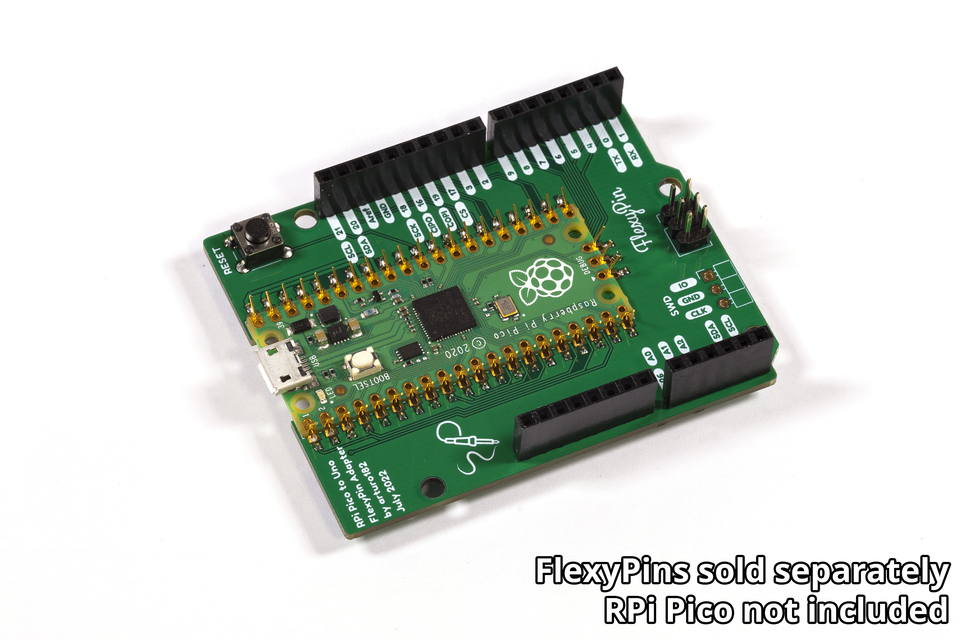
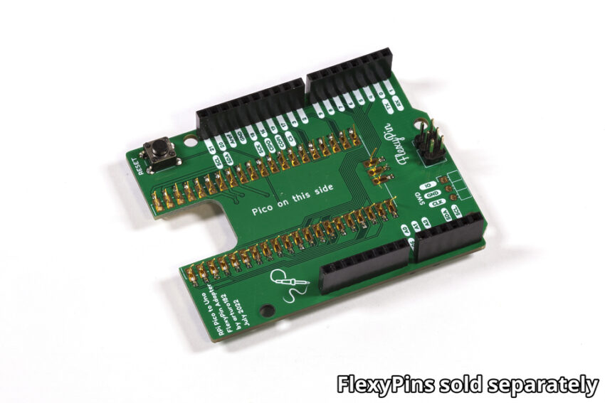
A Sweden-based consumer electronics and computers retail specialist, Solder Party has released its FlexyPin Adapter that gives the Raspberry Pi Pico an Uno form factor. With the help of FlexyPins, the board allows the Raspberry Pi Pico to be used with Uno shields without having to solder the Pico in place.
For castellated modules that have a pitch as low as 1.27mm, a connector pin called the FlexyPin has been designed. Since the footprint drills would be so close together, one might be able to use it with a 1.00mm pitch but it would require a more expensive PCB. The well-formed and gold-plated FlexyPins enable easy removal and insertion of modules without the hassle of soldering. They work great in many use cases such as testing, flashing, and others where the castellated modules are involved.
The Raspberry Pi Pico boards make use of 3.3V logic, whereas the Arduino Uno is 5V. The Raspberry Pi Pico is not 5V safe, hence the compatibility between an adapted Raspberry Pi Pico and an original Arduino is not one-to-one. In addition, it exposes fewer analog pins, which could provide a challenge for some shields, however, the pin-mapping was chosen specifically to support an 8-bit 3.5-inch 480×320 parallel LCD shield without any issues. The LCD shield is driven by making use of the RPi’s PIO along with the bb_spi_lcd library.
To push against the castellated pin headers of a Raspberry Pi Pico or wireless-capable Raspberry Pi Pico W, the FlexyPins which are available as an extra are soldered into the board. Furthermore, along with an extra Serial Wire Debug (SWD) connector which is added to the bottom of the board, the pins are brought out to the Arduino Uno-format headers.
From Solder Party’s Lectronz store, the Raspberry Pi Pico to Uno FlexyPin adapter can be ordered for $1.50. Additionally, the soldering kit includes a reset button, a set of socket headers, and an optional pack of 100 FlexyPins. Under the CERN Open Hardware License v1.2, the design files are available on GitHub.
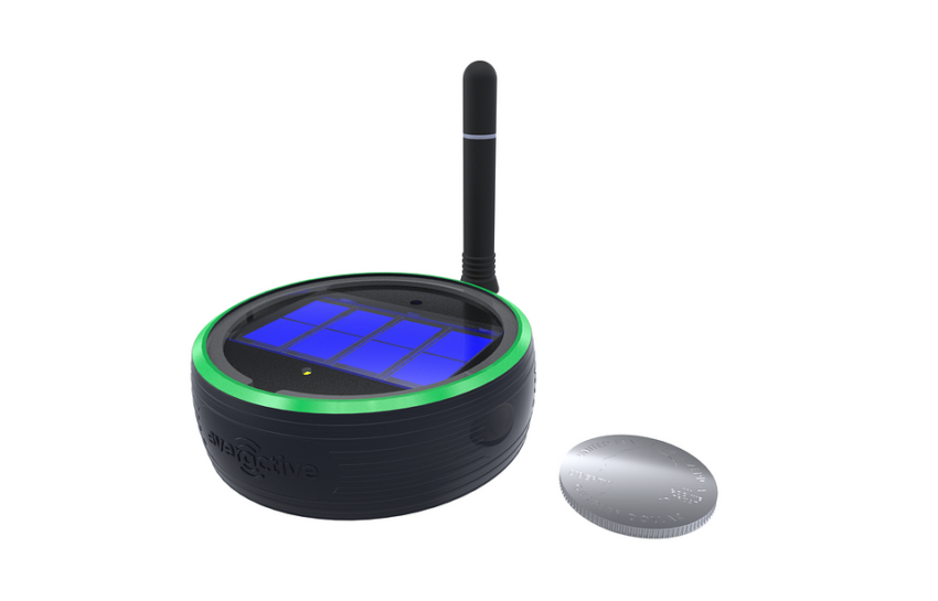
California-based IoT startup Everactive has announced the release of an ultra-low-power semiconductor and wireless IoT development kit with the ability to operate without a battery. This enables developers to leverage their onboard power to operate in distributed edge locations and also easily scale their Internet of Things applications without the constraints of any battery or power supply.
Everactive has included a development kit with two of the company’s patented batteryless IoT devices, each with a sensor suite that can simultaneously measure temperature, pressure, and a triaxial accelerator. The IoT development kituses a low-power indoor photovoltaic harvester as the only power source which makes it a batteryless IoT device. The hardware platform is capable of measuring and wirelessly transmitting data down to every 15 seconds.
“Our core breakthroughs in ultra-low-power wireless systems have overcome both the battery problems and networking issues that have plagued the IoT,” said Dr. Benton Calhoun, co-founder, and co-CTO at Everactive. “With that as the foundation, we then built an entire data delivery system specifically designed to manage the massive influx of new real-world data sets only made possible by batteryless technology. Ultimately, it is that data— and the derived insights— that matters to our developers and their end users.”
Everactive is achieving batteryless IoT hardware design through its patented energy harvesting solution that generates all the required power from multiple low-level energy harvesting sources, including indoor solar, thermal gradients, RF, vibration, and more. For seamless wireless communication, the company developed a mix of standard-compliant and proprietary integrated radios for broad data rates of up to several Mbps and communication ranges of kilometers.
Everactive Evernet is a wireless networking solution designed for high-density batteryless devices that takes advantage of the company’s always-on ultra-low-power receive that reduces power consumption while supporting thousands of devices with millisecond latency and 250+ meter non-line-of-sight range.
For more information on the product, you can consider reserving a spot for the evaluation kit. Everactive has started accepting orders for the batteryless IoT development kit and will begin shipping in November. According to public information, the hardware kit is sold at $599 which includes 2x ENV+ Eversensor, 1x USB Evergateway, and unlimited user accounts.
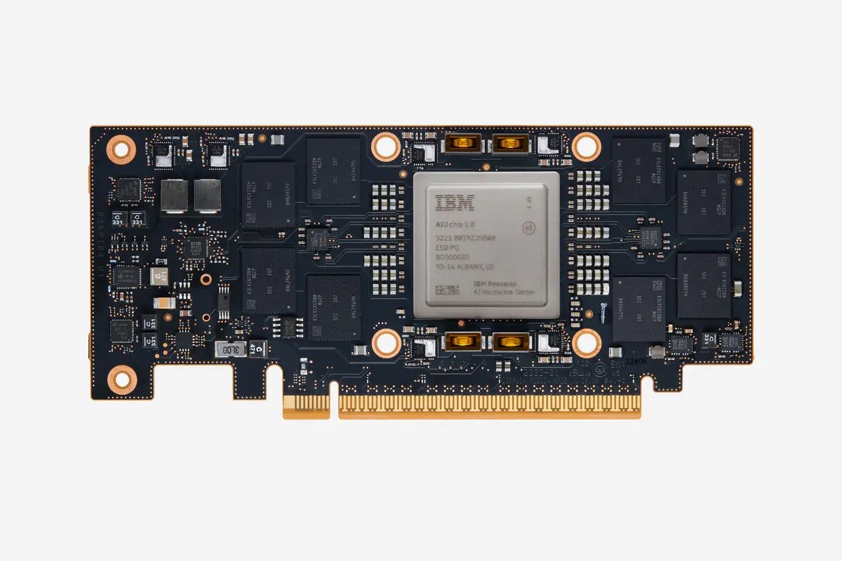
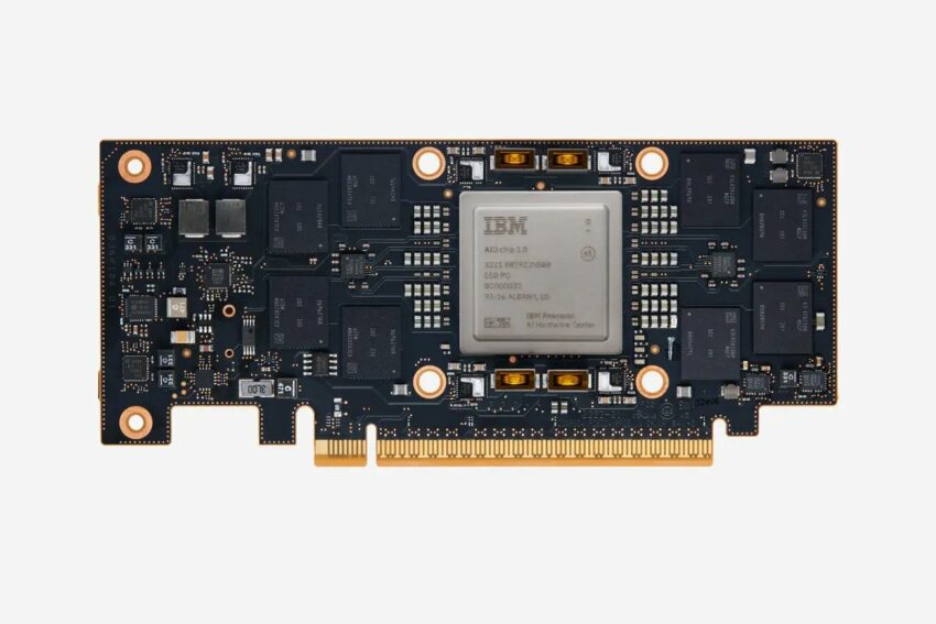
IBM believes that computing power and AI models have grown exponentially, but the supporting hardware to train them and run them on servers in the cloud or edge devices hasn’t advanced. IBM Research AI Hardware Center has decided to launch an application-specific integrated circuit for artificial intelligence that can be programmed to run any type of deep learning task– Artificial Intelligence Unit.
According to IBM, several manufacturers are looking for flexibility and high-precision CPUs that are suited for general-purpose software applications. But for deep learning models, high precision is something that puts the system at a disadvantage when it comes to training and running them, which requires massively parallel AI operations.
IBM took two paths to develop an application-specific integrated circuit that would be able to replace the central processing unit for deep learning tasks. One is to embrace lower precision as the company believes AI chips do not require ultra-precise because they are not calculating trajectories for landing a spacecraft on the moon. The second is that an AI chip should streamline AI workflows.
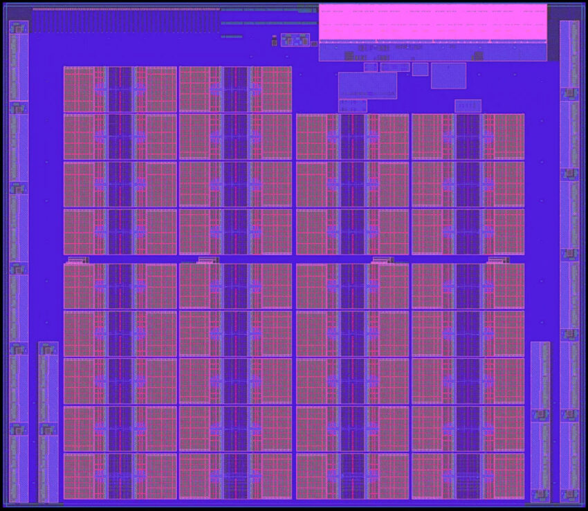
IBM Artificial Intelligence Unit is an upgraded and scaled version of the company’s proven AI accelerator built into its Telum chip. The hardware features 32 processing cores that resemble the AI core embedded in the Telum chip that currently powers the company’s z16 system. One of the other differences is that the new IBM AIU is faster with smaller 5nm transistors compared to 7nm in the Telum.
IBM led its efforts in the space of artificial intelligence with a mission to improve AI hardware efficiency by 2.5 times every year. By 2029, IBM aims to train and run AI models one thousand times faster than they could three years ago. IBM expects the Artificial Intelligence Unit to be one of the most significant landmarks in the journey of AI acceleration.
IBM is yet to provide internal details of the Artificial Intelligence Unit, but the enterprise-grade, industry-scale AI hardware is optimized for many types of matrix and vector multiplication operations. The company plans to reveal more details as time goes by.
In the first part of the “Fourier Analysis” article, we have focused on the properties and usages of the Fourier series. We have seen the power of Fourier series as a tool for both decomposing and constructing general periodic functions in terms of “pure” sines and cosines. The physical world, however, is full of interesting aperiodic or non-periodic functions as well as periodic ones. In course of historical development of the Fourier analysis concept, the original idea was extended to aperiodic signals. An aperiodic function never repeats, then it can technically be considered like a periodic function with an infinite period.
In the case of analysis of non-periodic signals, we can generalize the Fourier Series sum into an integral concept named the Fourier Transform. This is an integral transform in which the time domain signal has to be observed from minus infinity to plus infinity. The Fourier transform can also be considered as a special case of the Laplace transform.
The Fourier transform is a fundamental tool for Spectrum analysis. The best way to understand the true nature of a real-world signal is by examining its spectrum. Spectrum analysis is a very important topic in many scientific and technical fields such as biology, astronomy, geo-sciences, and especially in the field of digital signal processing (DSP).
A Brief Review on Complex Numbers and the Phasor Diagram
The concept of ‘complex numbers’ is out of the scope of this article and we just needed it to achieve the main idea. You could refer to the link attached to get more information:
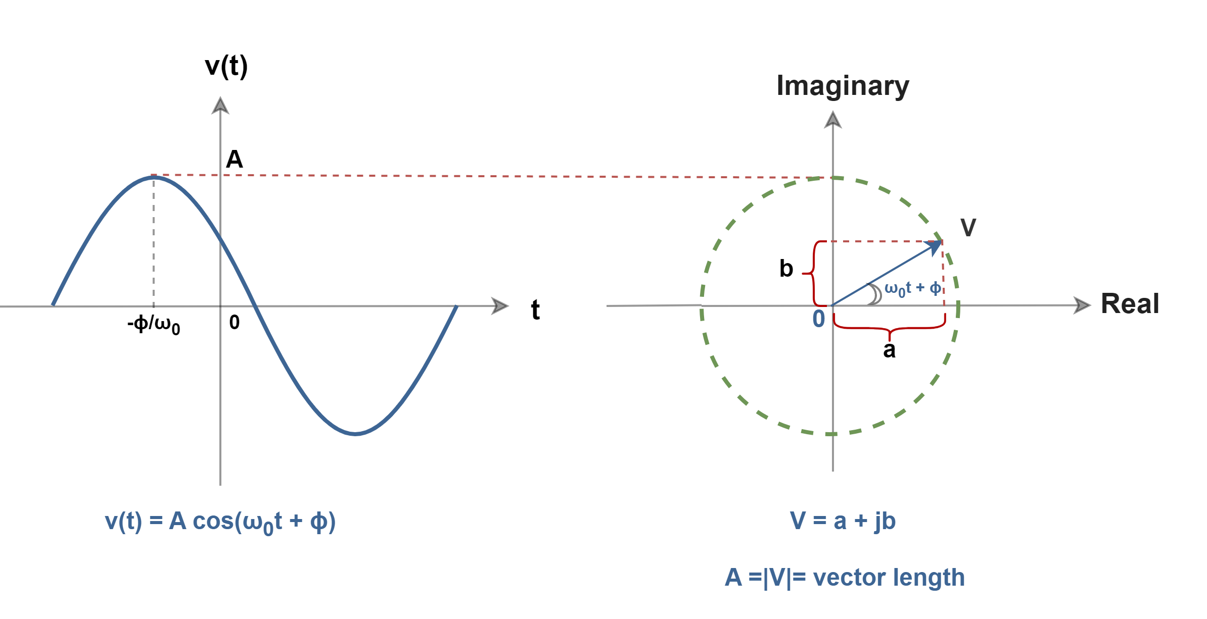
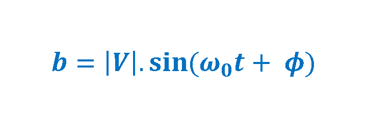
We now define a complex quantity called a “phasor,” which applies to functions that vary sinusoidally with time, like voltages and currents. A phasor is a rotating vector at a constant velocity. Its magnitude corresponds to the amplitude of a signal. It has one end arrowed, to show the direction of action of the quantity. In the vector diagram in Figure 1, the vector of a sinusoidal quantity (V) can be obtained by the vectorial addition of the real (a) and imaginary parts (b), i.e. of the sine and cosine components.
Figure 1: Vector (Phasor) diagram of a sinusoidal signal
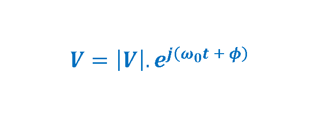
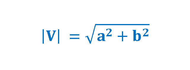
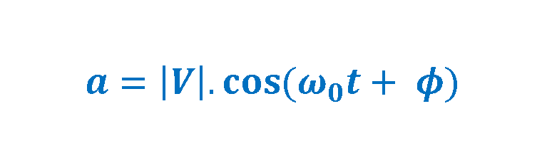
Using Euler’s formula, the polar description of the complex number ‘V’ is given by a magnitude |V| and an argument (ω0t + ϕ) and satisfies formulas in the set of Equations 1-1 to 1-4:
Equation 1-1: Definition of the complex number VEquation 1-2: Calculation of the magnitude of VEquation 1-3: Calculation of the cosine component of VEquation 1-4: Calculation of the sine component of V
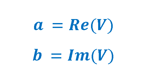
As already mentioned, ‘a’ equals the real part of the complex vector ‘V’ and ‘b’ equals the imaginary part of it. Equation 2 explains these relationships:
Equation 2: Definition of the real and imaginary parts of V
The Fourier Transform
The Fourier transform is used similarly to the Fourier series, in that it converts a time-domain function into a frequency-domain representation. However, there are a number of differences:
Fourier transform can work on aperiodic signals.
Fourier transform is an infinite sum of infinitesimal sinusoids.
Non-periodic signals do not have a line spectrum but a continuous spectrum.
Fourier transform has an inverse transform, that allows for conversion from the frequency domain back to the time domain.
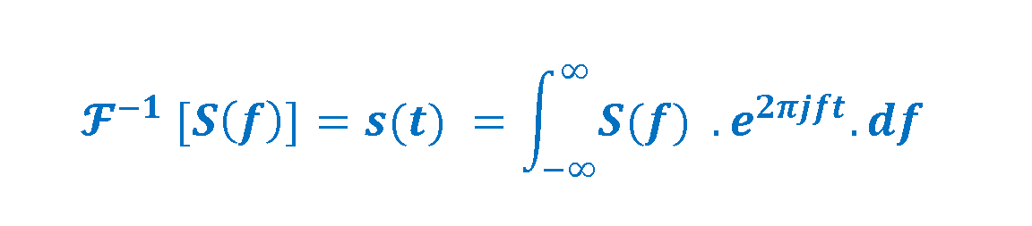
The Fourier transform (or Fourier integral transform) of a function s(t) can be applied by the following integral in Equation 3:
Equation 3: Definition of the Fourier transform of the function s(t)
Thus, S(f) represents the frequency domain analysis of the time domain signal s(t) by providing the amplitudes of its frequency components. Equation 3 is also called the forward Fourier transform of the function s(t).
The Inverse Fourier Transform supplies a single real-time-domain signal again from the complex spectrum in the reversed procedure. The inverse transform is given by a similar integral in Equation 4:
Equation 4: Definition of the inverse Fourier transform of the function S(f)
Using these formulas, the aperiodic time-domain signals can be converted to and from the frequency domain, as needed. In the concept of Fourier transforms the pairing metaphor is essential (between equations 3 and 4) so, there is a special notation in many texts to symbolize the bi-directional transforms, as shown in Equation 5:
Equation 5: The Fourier transform pairs notation
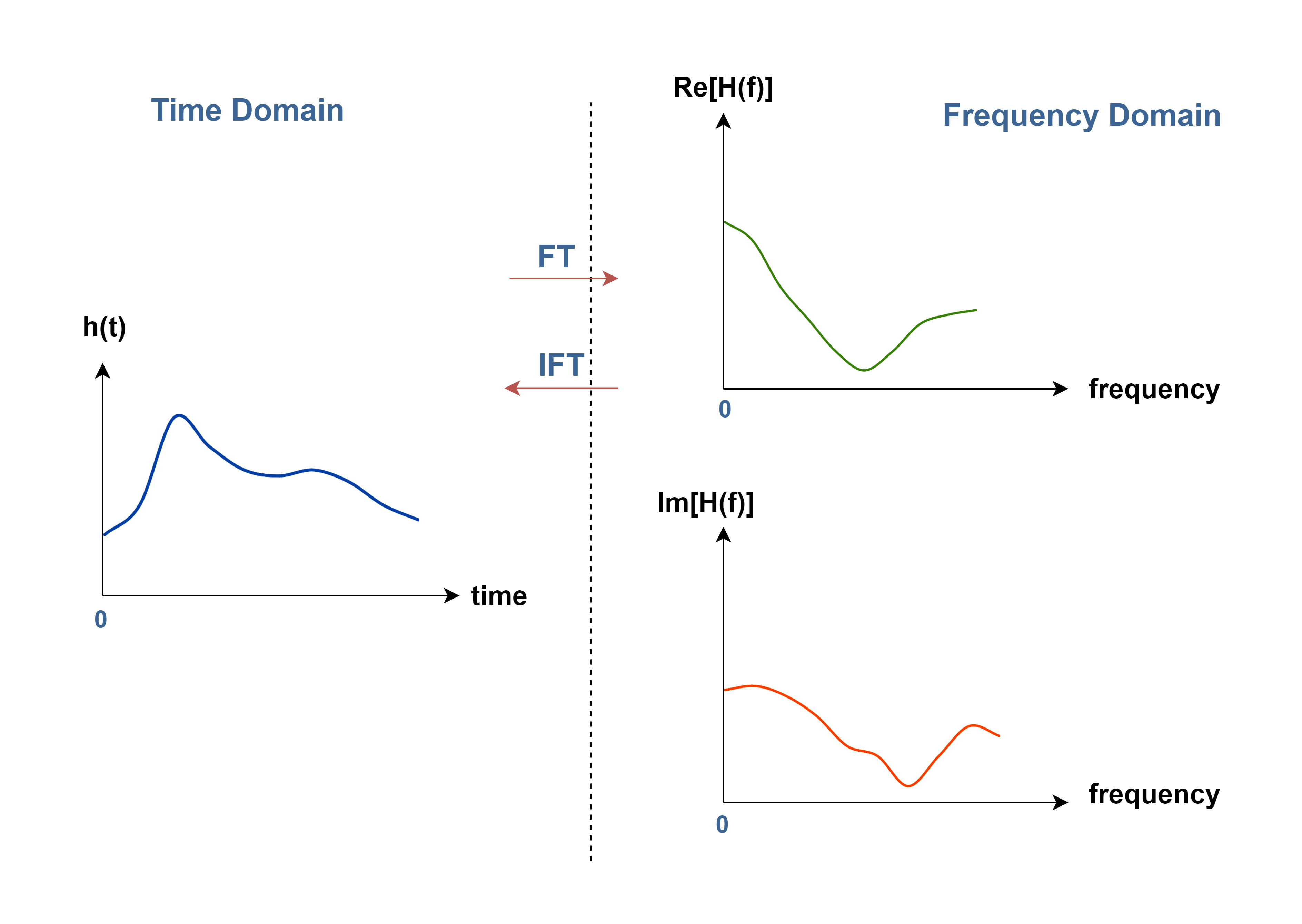
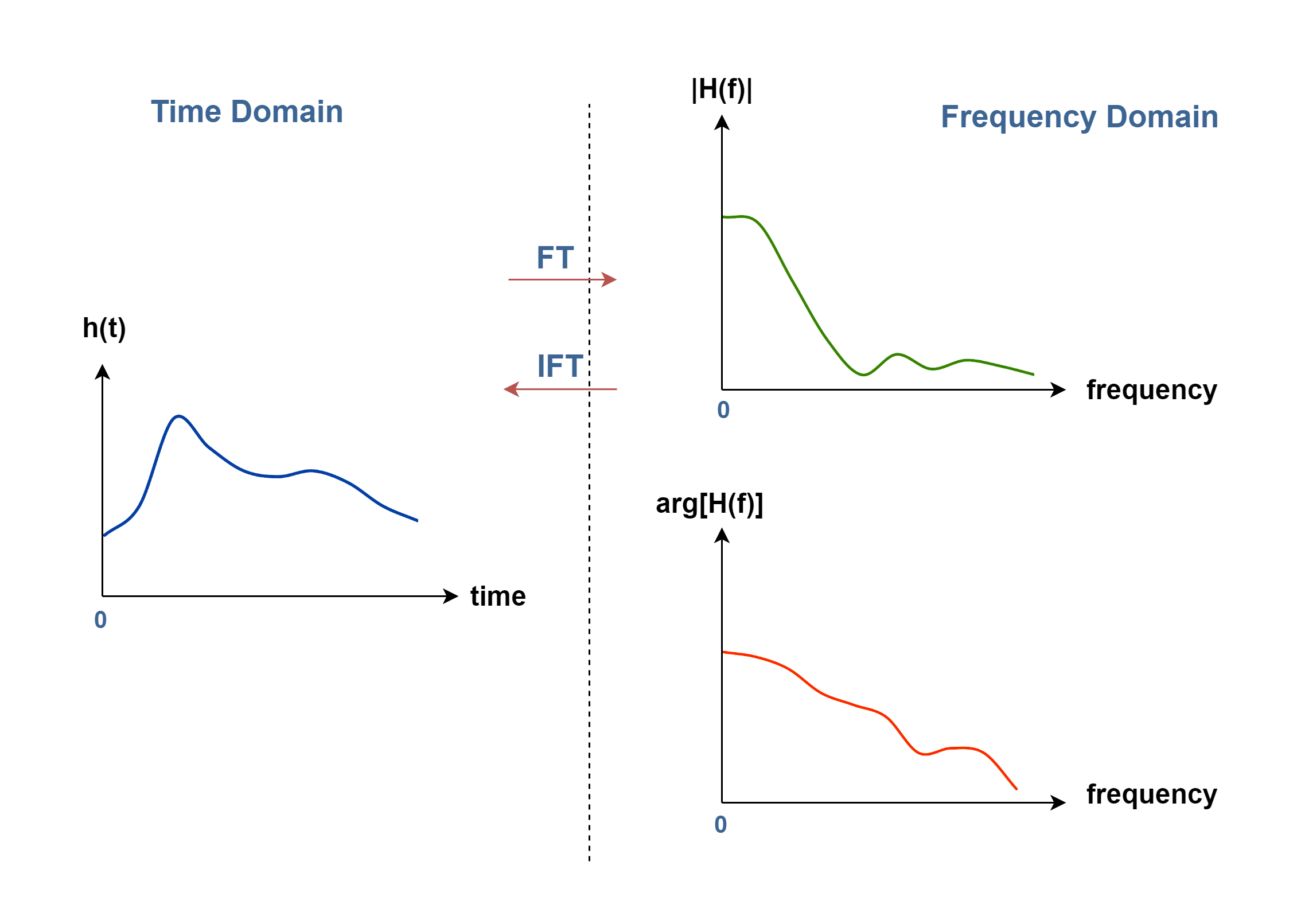
The Fourier transform (FT) alters a real-time-domain signal into a complex spectrum in the frequency domain which is composed of the real-part and the imaginary-part components. The real part accurately describes the amplitude of the cosine component and the imaginary part precisely describes the amplitude of the sine component. Figure 2 explains the transform mechanism graphically for a non-periodic function h(t).
Figure 2: The real part and the imaginary part characteristic
In most of the applications, for each frequency, the magnitude of the vector represents the amplitude of a complex sinusoid with that frequency, and the argument of the complex value represents that complex sinusoid’s phase offset. The graphs of the magnitude and the phase in terms of frequency represent the spectrum of the non-periodic signal. Figure 3 shows the spectrum magnitude |H(f)|and the argument of the function [arg(H)] of an arbitrary signal h(t).
Figure 3: The magnitude and phase (argument) characteristic
The parameters of the magnitude and the phase (argument) of the transformed vector H(f) are calculated in Equations 6-1 and 6-2.
Equation 6-1: Calculation of the magnitude of H(f)Equation 6-2: Calculation of the argument of H(f)
As already mentioned, when we want to consider the spectrum, in most cases we are mostly looking at the magnitude in terms of frequency rather than phase (or argument).
Examples of Fourier Transforms and Their Graphical Representations
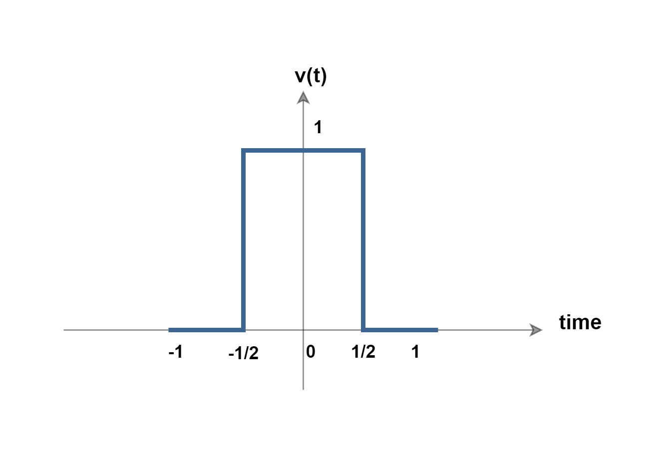
For a better understanding of the mechanism of the Fourier transform, we consider transforms of some specific functions. First, we observe a non-periodic square-shaped function called a single square pulse as shown in Figure 4.
Figure 4: The square pulse
This function can be defined by Equation7:
Equation 7: The mathematical model for the square pulse
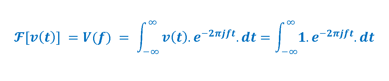
If we apply the Fourier transform to this function, we can write Equation 8-1 to calculate the transform:
Equation 8-1: Calculation of the Fourier transform
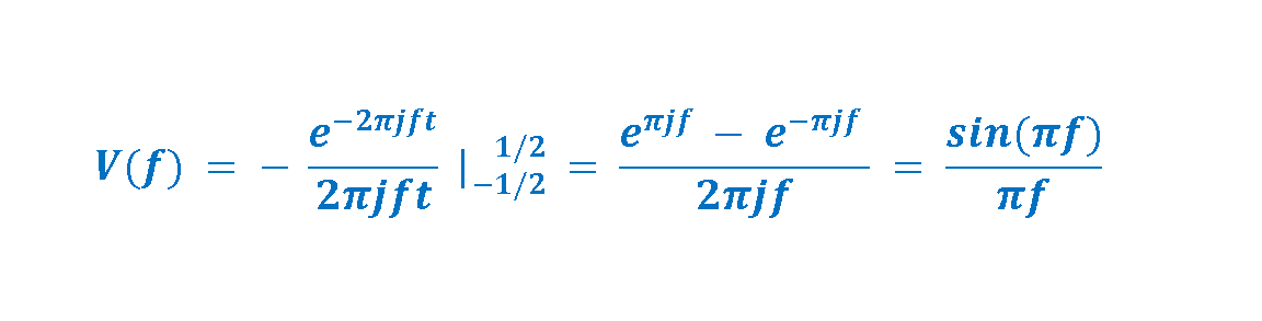
Finally, the result is obtained as Equation 8-2:
Equation 8-2: Calculation of the Fourier transform
Where the result is simplified by using Euler’s identity to replace two complex exponentials.
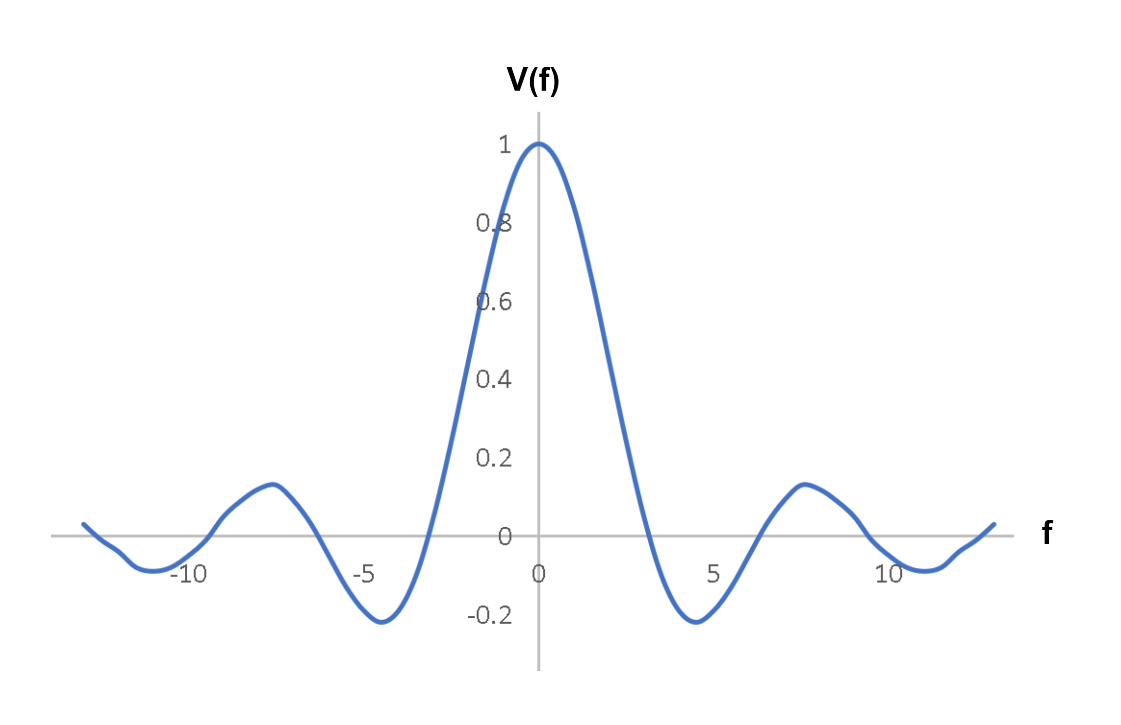
The graph of this V(f) is shown in Figure 5:
Figure 5: The Fourier transform of the square pulse
This curve represents one of the classic Fourier transforms with the special function which is called Sinc. Generally, this function is defined as in Equation 9-1 and 9-2:
Equation 9-1: Definition of the sinc functionEquation 9-2: Specific numerical values of the sinc function
Therefore, we can write our resultant in terms of the Sinc function as in Equation 10:
Equation 10: Mathematical model for the Fourier transform of a square pulse
One property is clear V(f) seems to exist for all values of frequency. The spectrum mathematically consists of positive and negative frequencies, although, the negative frequency range does not practically provide any additional information about the original time domain signal.
One of the important examples of the Fourier analysis is the unit impulsefunction which is also called the Dirac delta distribution. In mathematics, the Dirac delta distribution (δ) is a generalized function over the real numbers, whose amplitude value is zero everywhere except at zero. Equation 11 gives the definition of this function:
Equation 11: The definition of this Dirac delta function
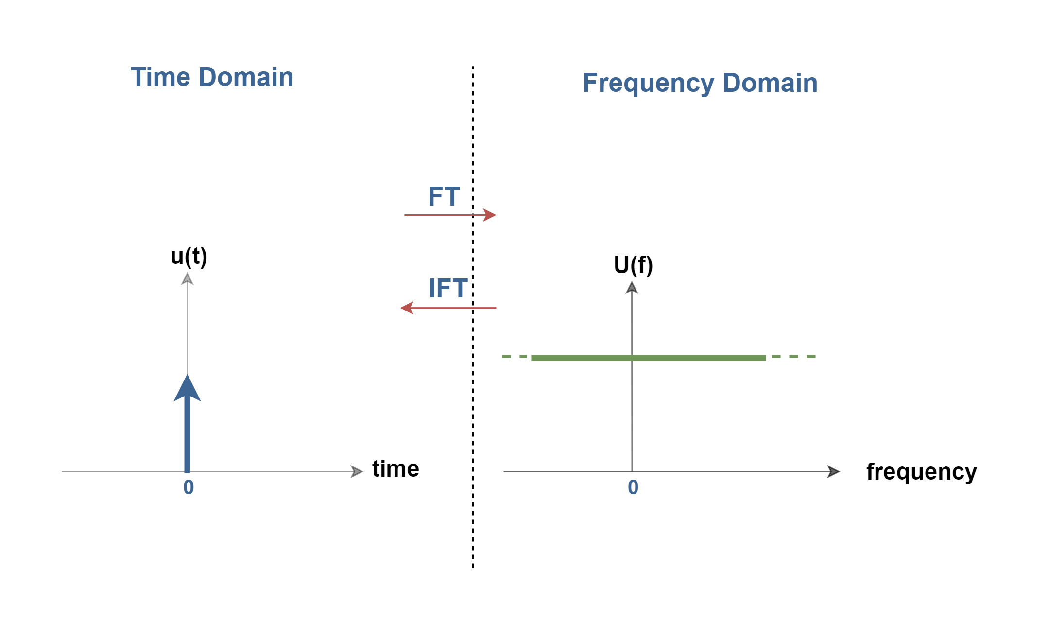
We observed that the spectrum of a single square-wave pulse is a sin(x)/x function. It can be imagined that if the pulse width T0 is allowed to become narrower to tend towards zero in the time domain, all zero-crossing points of the sin(x)/x function in the frequency domain will tend towards infinity. In the time domain, this provides an infinitely short pulse, a so-called Dirac impulse, the Fourier Transform of which is a straight horizontal line; i.e. the energy of the signal is distributed uniformly from zero frequency to infinity. Figure 6-1 shows u(t) as a unit impulse signal (with an arrow in the graphical representation) and its spectrum as U(f).
Figure 6-1: The Fourier transform of a Dirac delta function
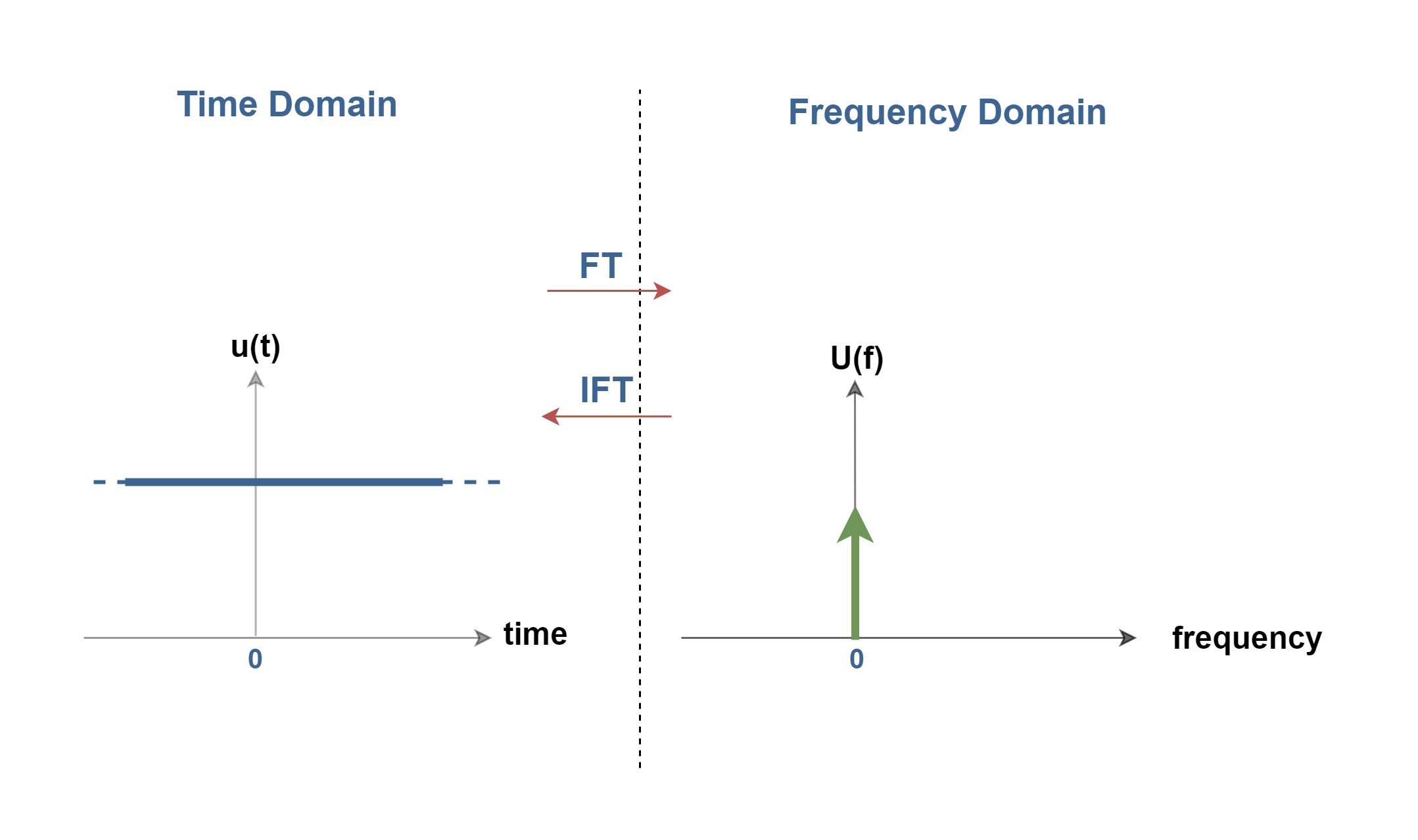
Conversely, a single Dirac needle at f=0 in the frequency domain corresponds to a direct voltage (DC) in the time domain.
Figure 6-2: The Fourier transform of a DC signal
Relations Between the Transform and the Inverse Transform
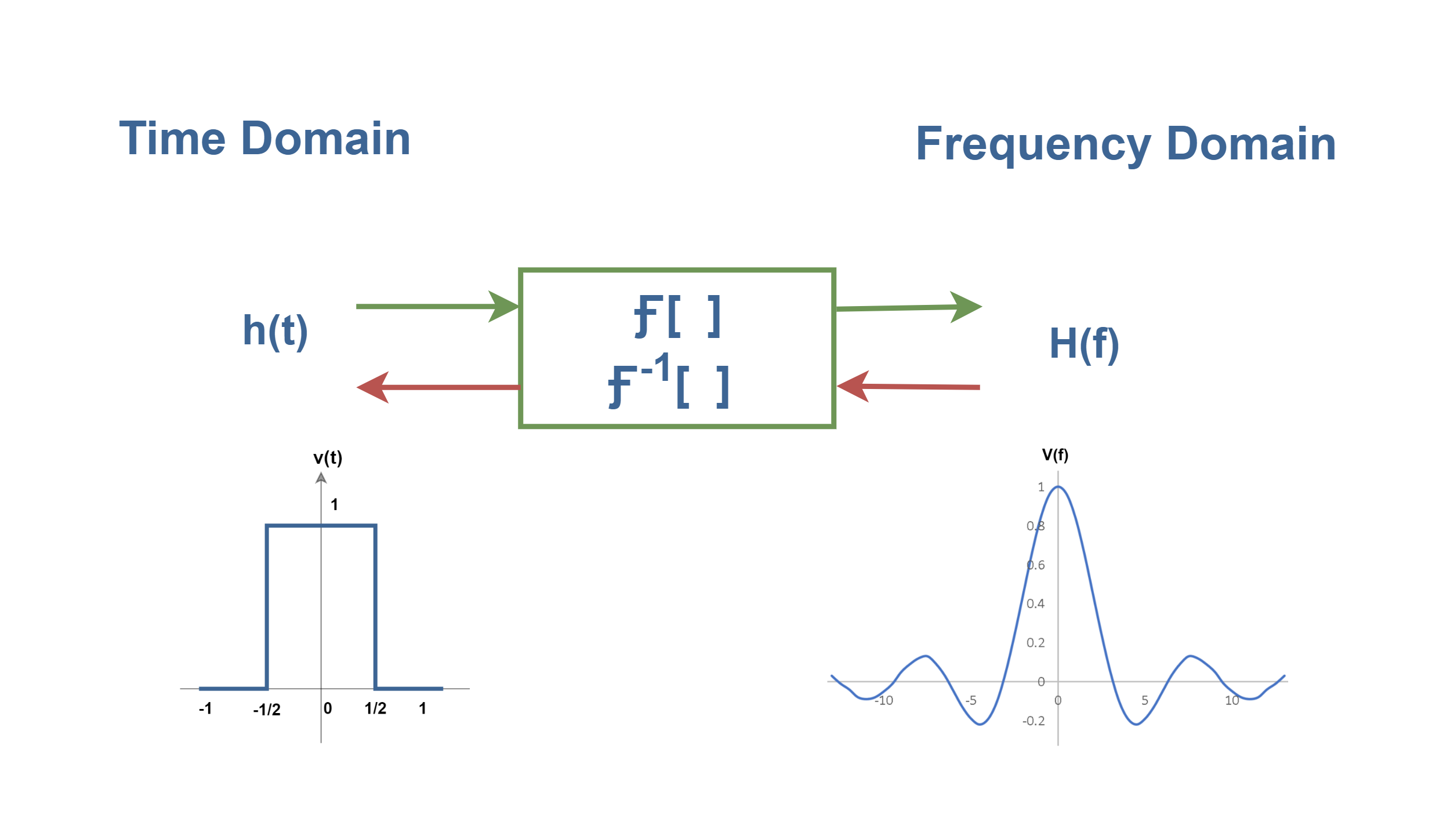
Transforms can be equally well specified either analytically (i.e. by a formula) or graphically. Therefore, we may think of the Fourier transform as a black box or a system whose inputs and outputs are graphs. The central idea of this view is that transforms are functions indeed. The difference is that for a transform, the inputs and outputs are not numbers, but other functions.
The transform pair is completely defined by displaying the respective graphs of the time-domain function as the input and the frequency-domain function as the output (or vice versa) by giving their formulas.
For example, we could view the relationship between the square pulse and its Fourier-transformed function (a sinc function) as shown in Figure 7:
Figure 7: The functional block diagram of the transforms pairs
Conclusion
The Fourier Transform calculates the variation of the real components and the variation of the imaginary components versus frequency from the time-domain signal.
The time and frequency parameters of pulsed signals are related in a mutual fashion. This is called the reciprocal spreading principle of signals between time and frequency domains in the Fourier transform concept. It simply means that a wide pulse has a narrow spectrum, whereas a narrow pulse has a wide spectrum. Also, as a spectrum gets wider, its amplitude gets smaller. Using such reciprocal-spreading relationships permits easy time-to-frequency and frequency-to-time conversions.
Now, we can conclude that the Fourier series, i.e. the analysis of the harmonics, is nothing else than a special case of a Fourier Transform where the Fourier Transform is simply applied to a periodic signal and the integral can then be replaced by a summation formula. The information over one period is sufficient for the integration.
Summary
A transform allows us to see a signal from a different dimension or point of view.
The Fourier series and its further refinements, such as the Fourier transform, are a form of math that takes a function of one variable (such as time) to another (such as frequency). Hence this type of process is classified as a transform.
For the nonperiodic signalthe spectral band contains spectral amplitude values not only at certain points but at all points.
Apart from the fact that a phasor rotates, it has exactly the same properties as any other vector.
The Fourier transform of a function is a complex-valued function representing the complex sinusoids that contain the original function.
This transform provides information about the real part, i.e. the cosine component, and the imaginary part, i.e. the sine component, at any point in the spectrum.
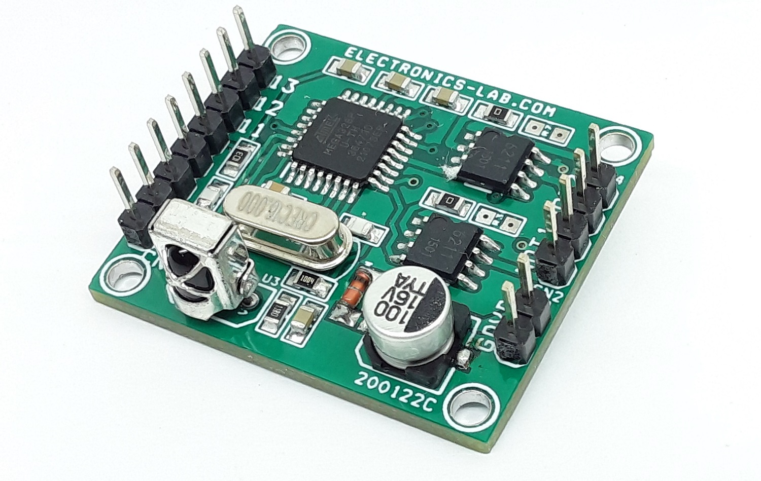
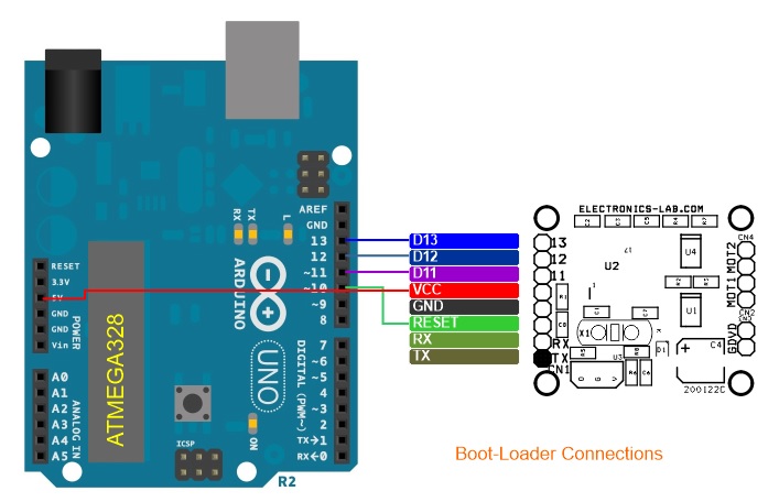
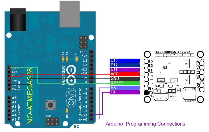
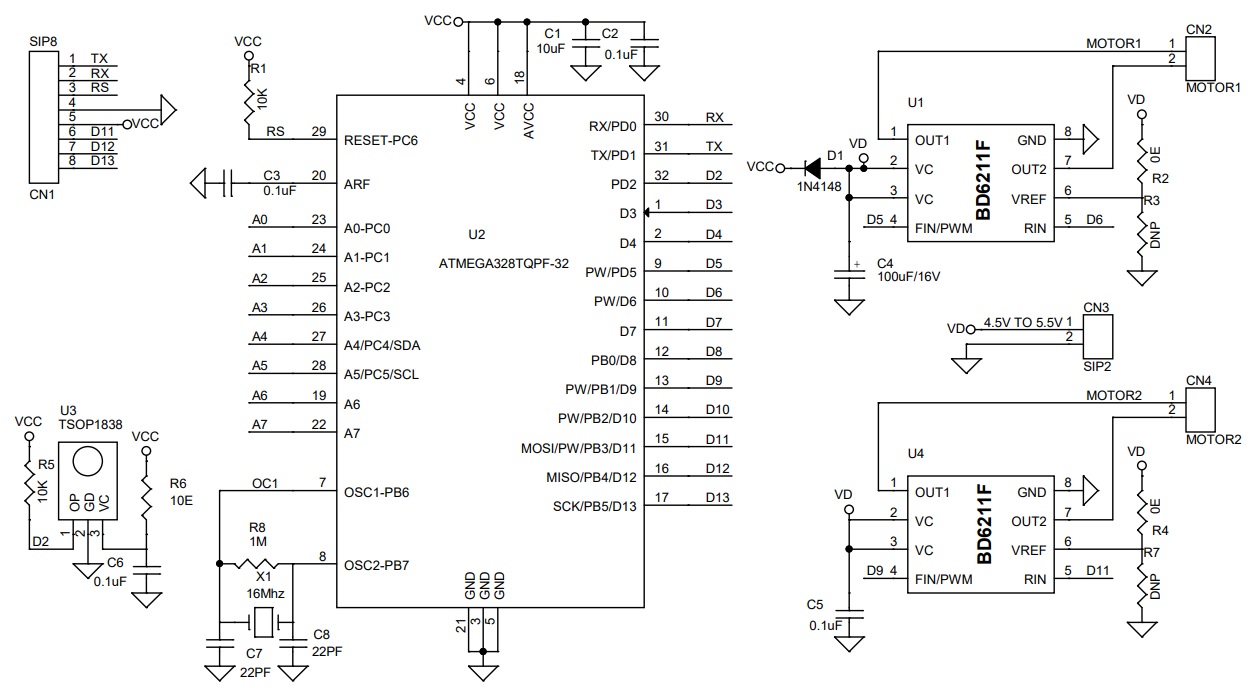
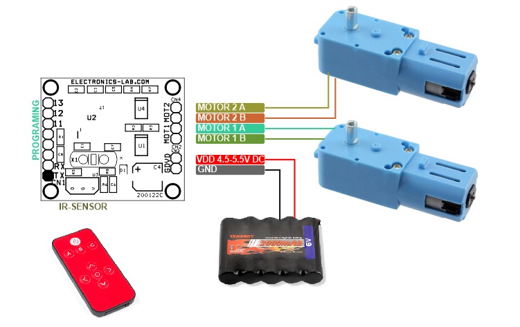
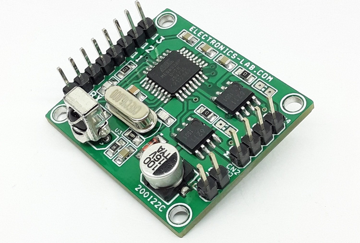
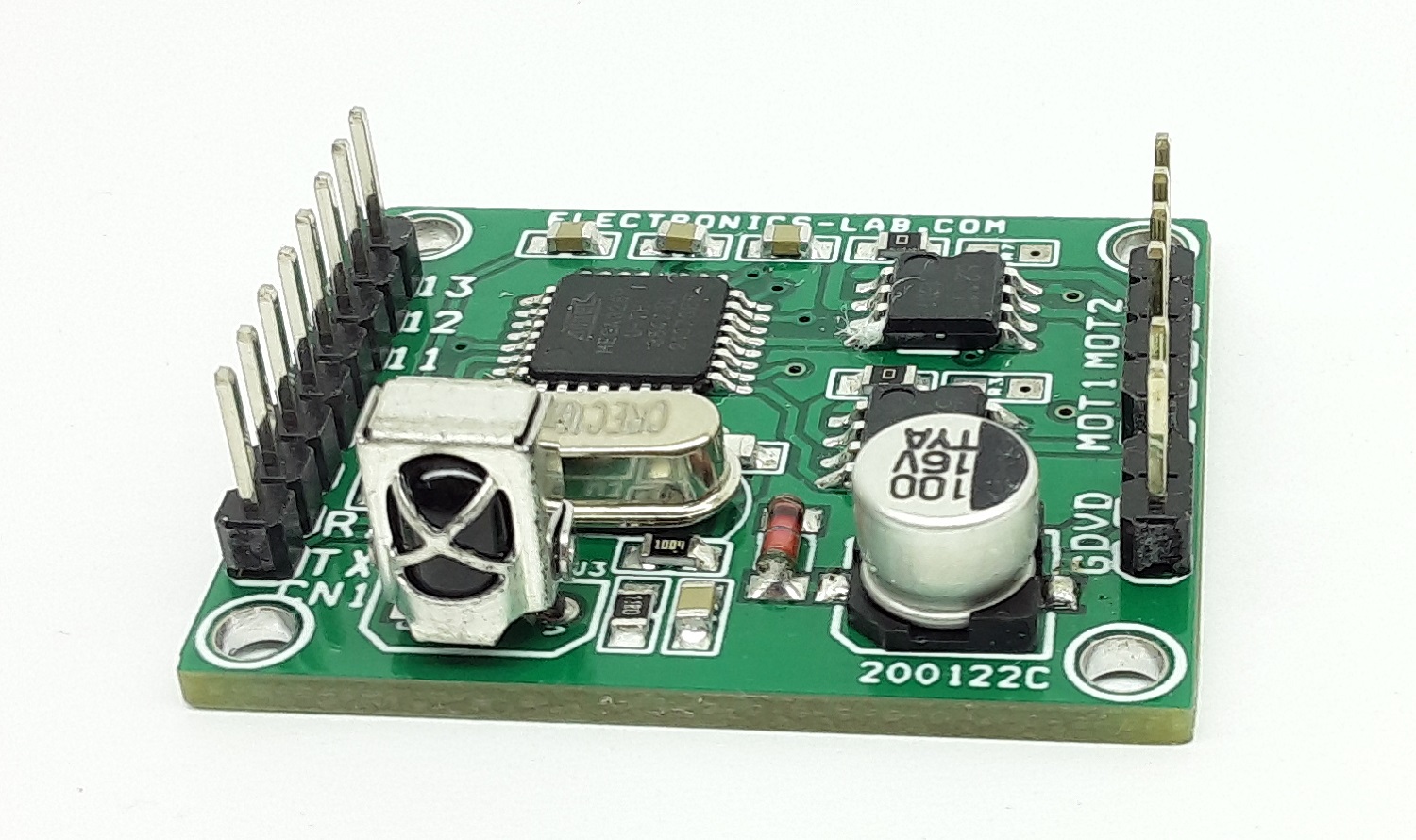
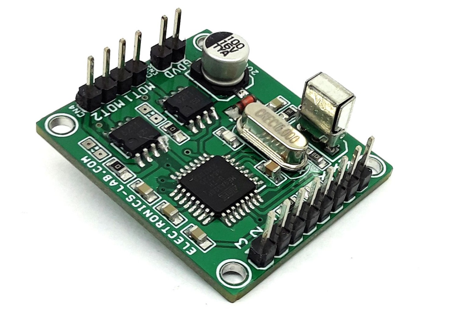
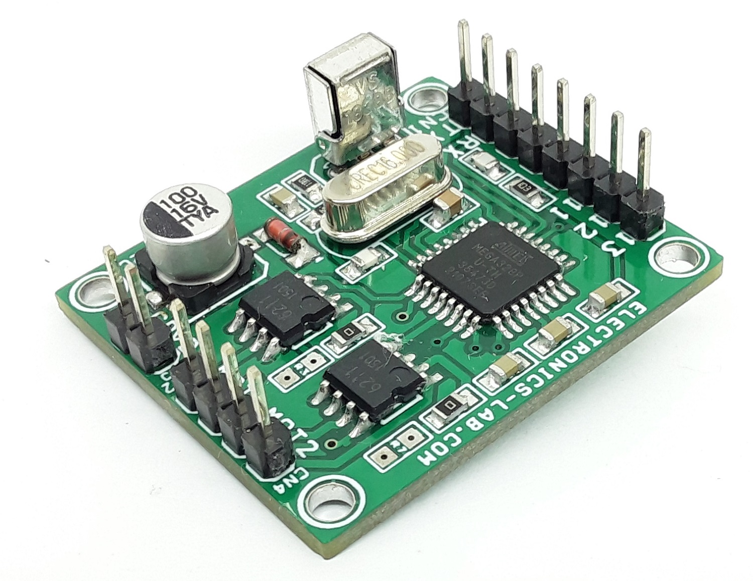
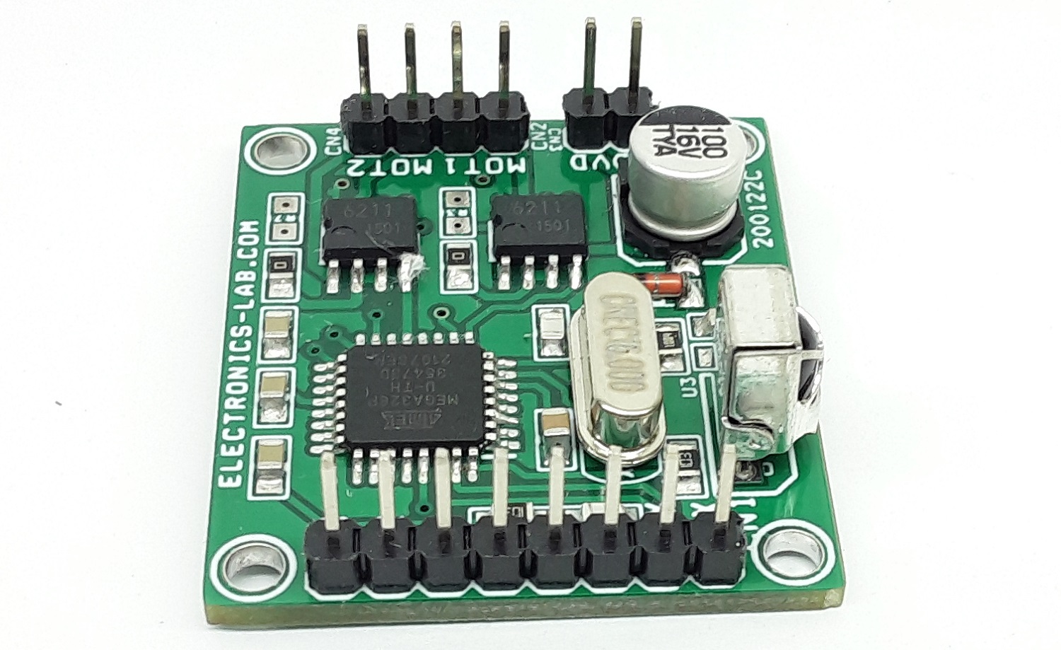
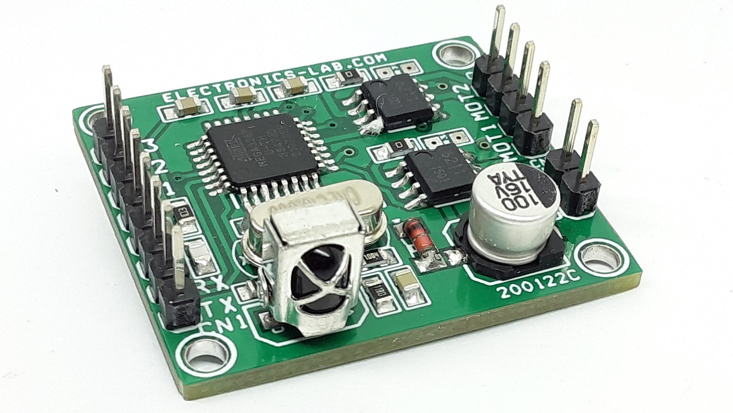
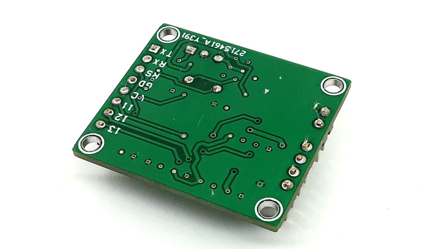
The Robot Controller is a very compact solution for controlling small and medium size robots using an Infrared remote. The project is fully Arduino compatible and consists of an ATMEGA328 microcontroller, 2 x BD6211 motor drivers, TSOP1838 IR sensor. BD6211 H-bridge is a full bridge driver for brush motor. The reference pin of BD6211 is pulled high and needs 2 x input to control the direction of the motor. 2 input pins of BD6211 are connected to ATMEGA328 for direction control of the motor. The project can be used to drive dual motors for 3-wheel robots or 4 x mini-DC motors. Input power supply 4.5V to 5.5V DC, the project can drive load up to 1A for each channel. Connector CN1 is provided to program the ATMEGA328 chips using Arduino IDE.
Arduino Code
Arduino example code is available as a download to test the board. With this code user will be able to drive 3-wheel robot with 2 Motors, and 5 functions Forward, Reverse, Turn Left, Turn Right, and Stop
Follow bellow link to learn more about programming and boot-loader burning for a new ATMEGA328 chip.
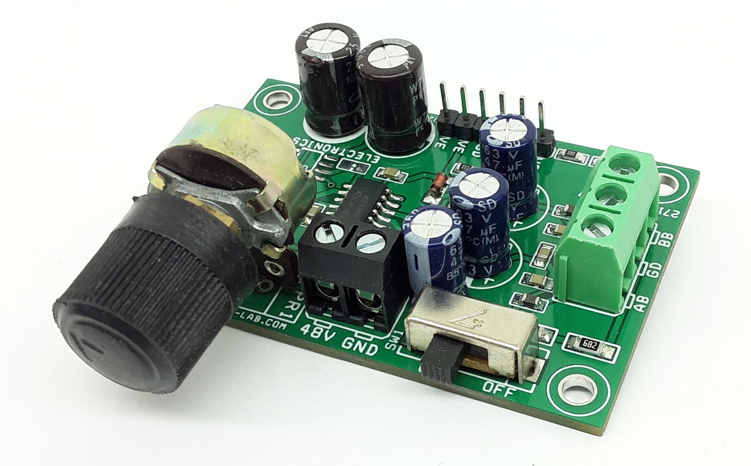
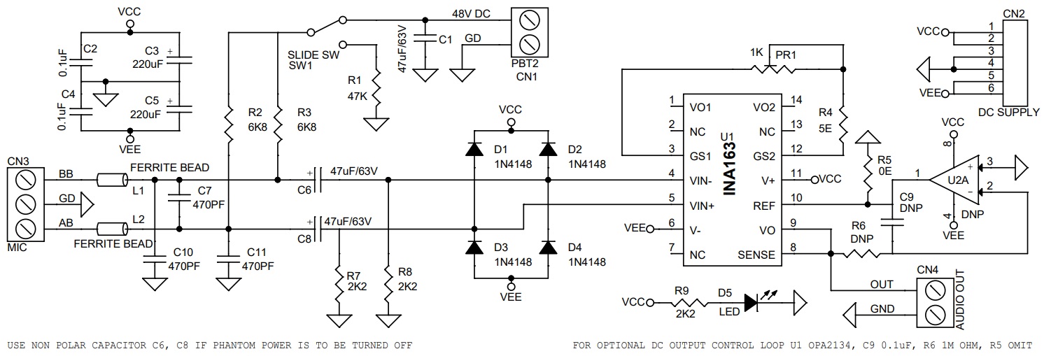
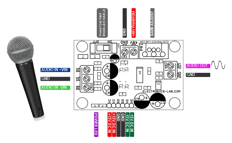
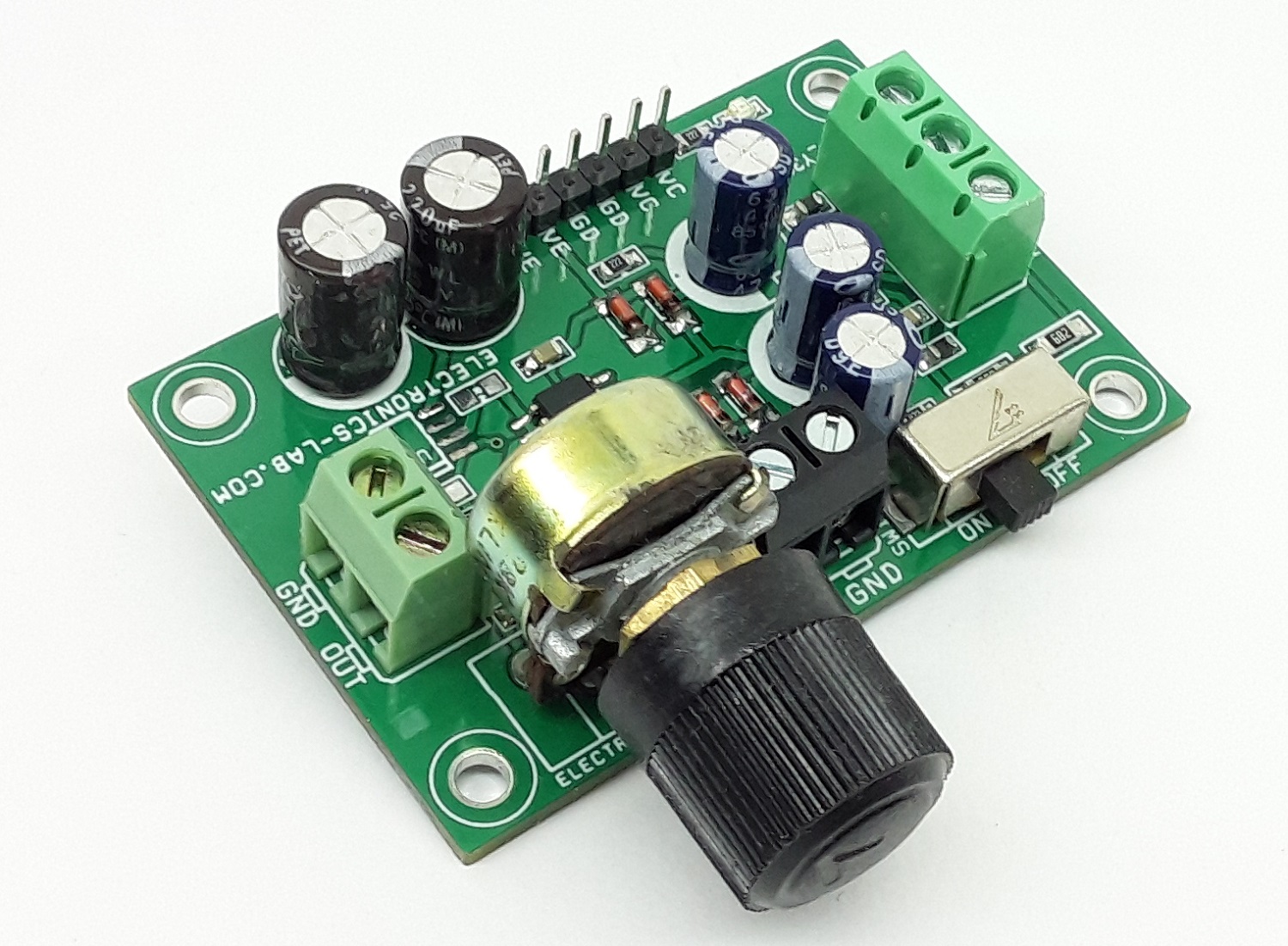
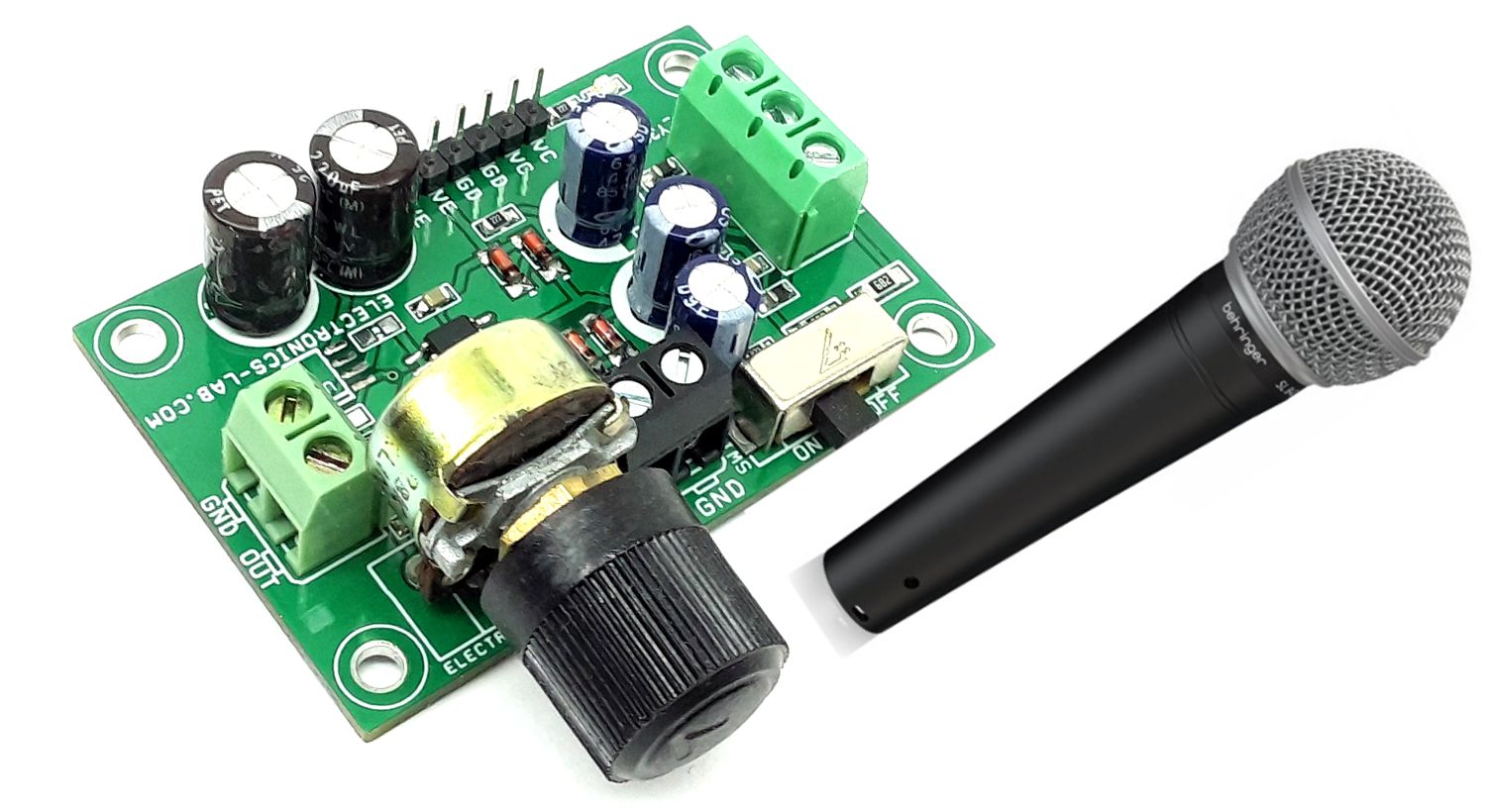
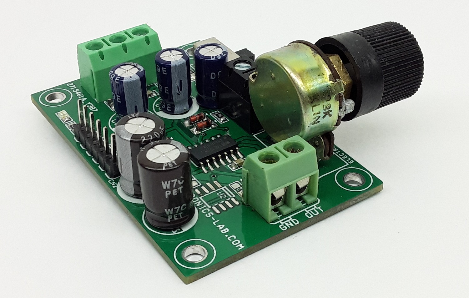
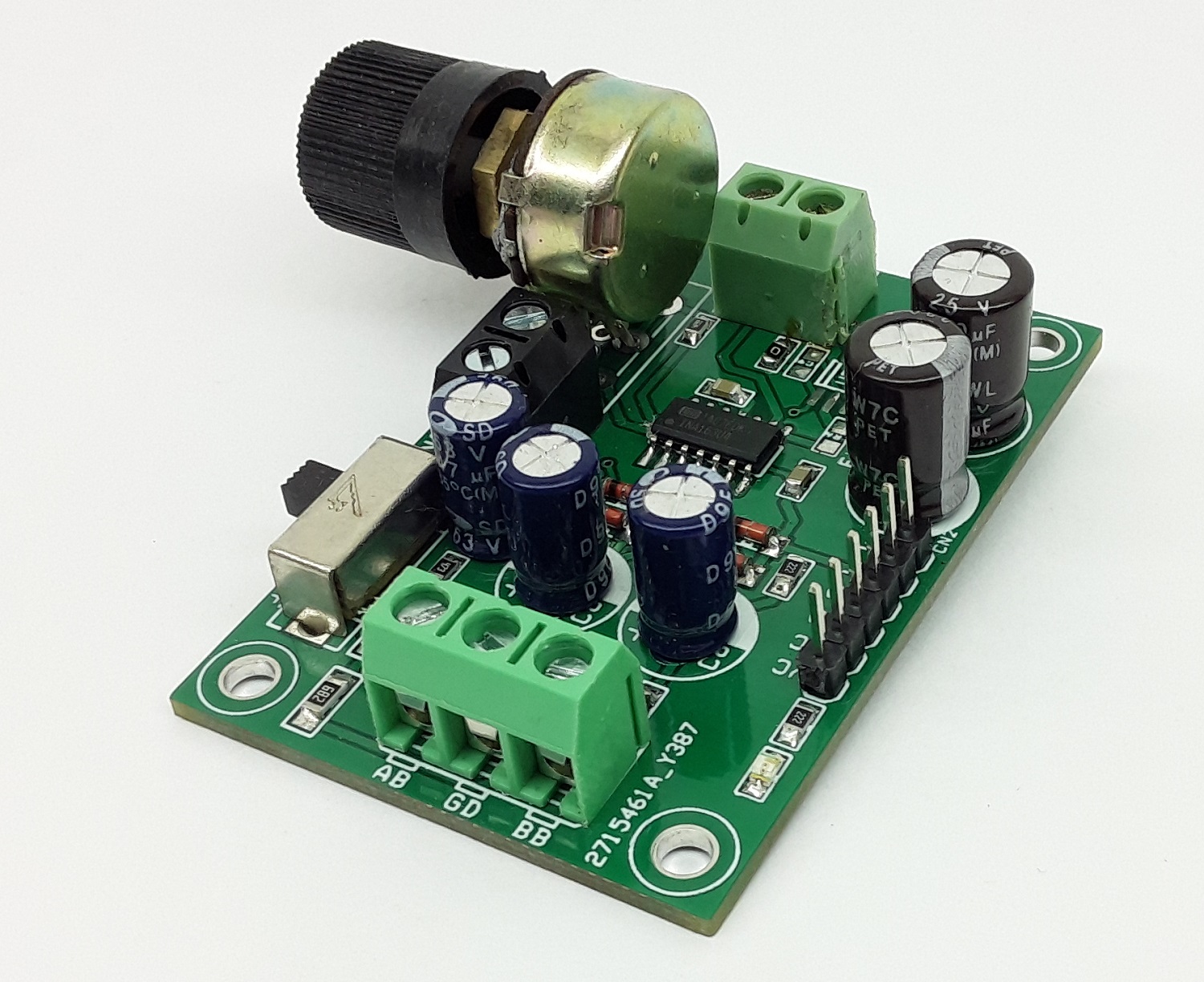
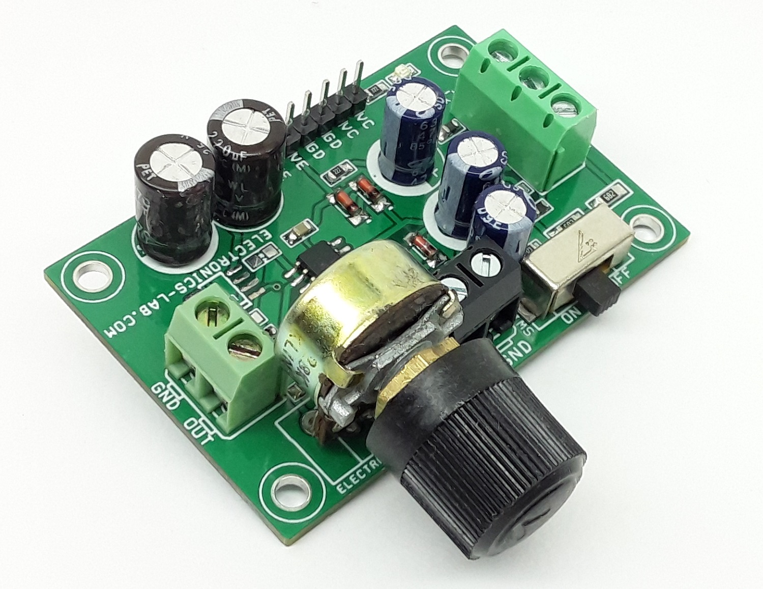
The project presented here is a professional quality Phantom powered Microphone pre-amplifier. The project is built using the INA163 chip from TI. The Chip is a very low-noise, low-distortion, monolithic instrumentation amplifier. R2 and R3 provide a current path for a conventional 48V phantom power source for a remotely located microphone. A slide switch SW1 allows phantom power to be disabled. C6 and C8 block the phantom power voltage from the INA163 input circuitry. Additional input protection against ESD and hot-plugging, four 1N4148 diodes D1, D2, D3, D4 connected from the input to supply lines. R7 and R8 provide a path for the input bias current of the INA163. Gain is set with a variable resistor, PR1, in series with R4. R4 determines the maximum gain. The total resistance, R4 + PR1, determines the lowest gain. A special reverse-log taper potentiometer for PR1 can be used to create a linear change (in dB) with rotation. LED D5 is used as a power indicator. L1, L2, C7, C10, and C11 components protect the inputs from EMI and RFI noise.
Optional DC Output Control Loop
Input offset current (typically 100nA) creates a DC differential input voltage that will produce an output offset voltage. This is generally the dominant source of the output offset voltage. With a maximum gain of 1000 (60dB), the output offset voltage can be several volts. This may be entirely acceptable if the output is AC-coupled into the subsequent stage. An optional circuit is provided to tackle this problem. An inexpensive FET-input op-amp U2A in a feedback loop drives the DC output voltage to 0V. Op-Amp is not in the audio signal path and does not affect signal quality.
Install the Following Components for DC Output Control Loop
U2A = OPA2134 SOIC8
C9 = Ceramic Capacitor 0.1uf/50V SMD Size 0805
R6 1Mega Ohm 5% SMD Resistor Size 0805
Omit Resistor R5
Connections and Other Details
CN1: Pin 1 = +48V DC Phantom Power Input, Pin 2= GND
CN2: Pin 1-2 = VCC +15V DC, Pin 2-3 = GND, Pin 4-5 VEE -15V DC