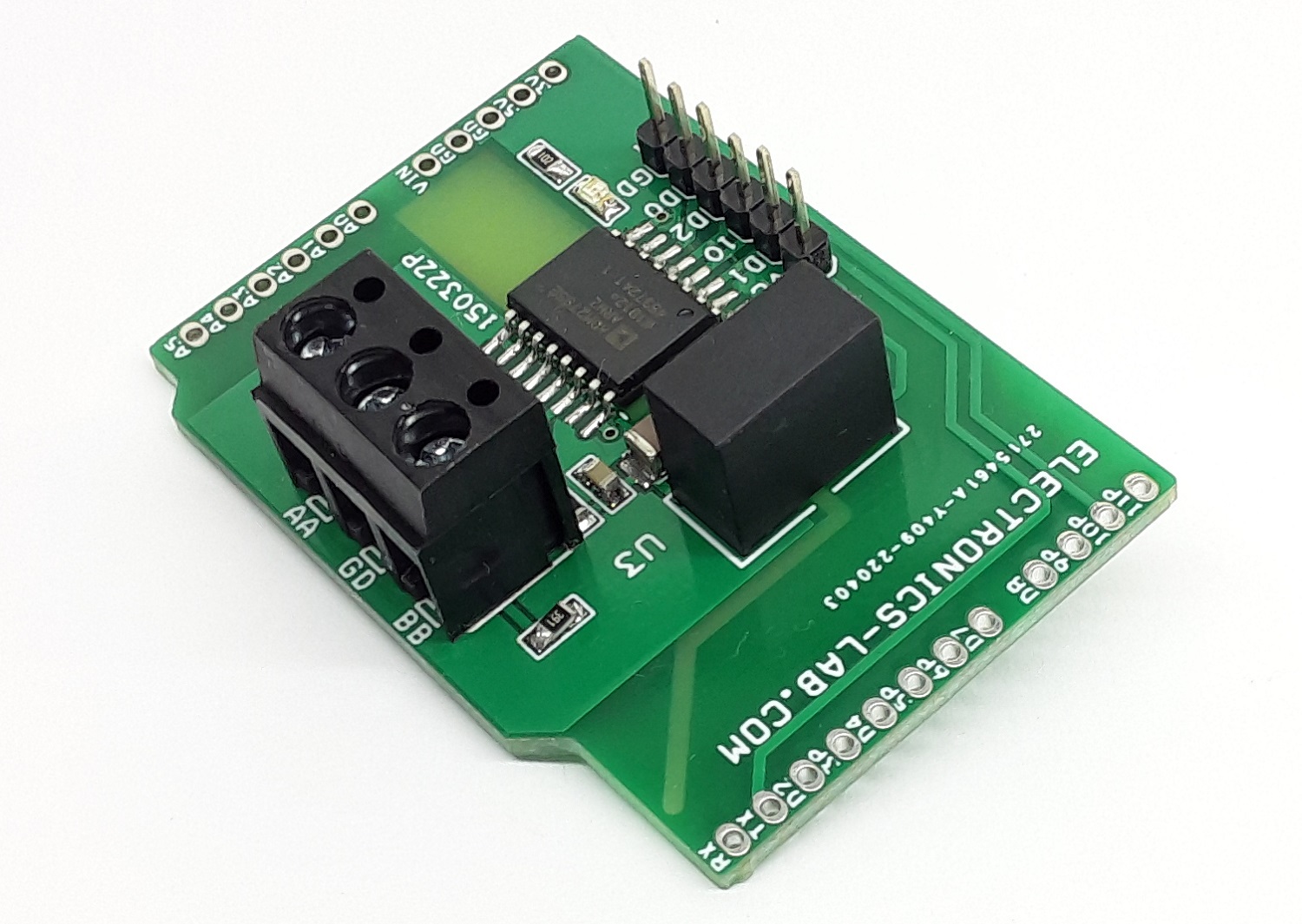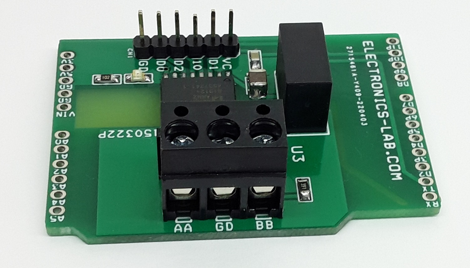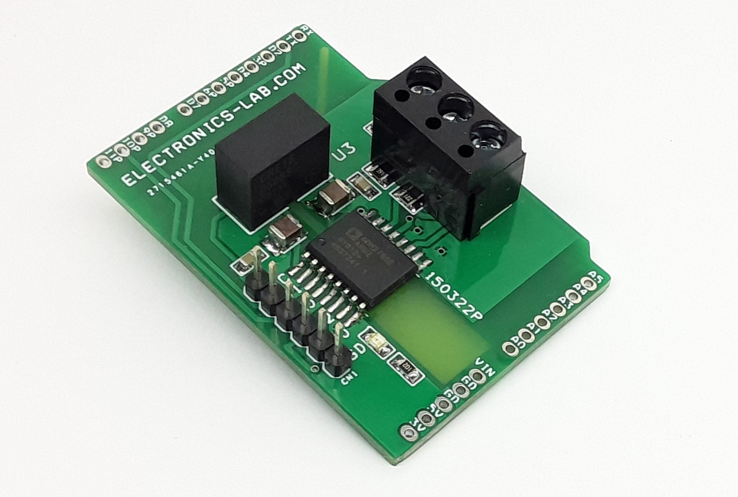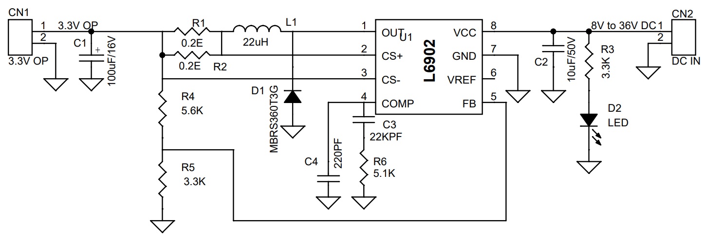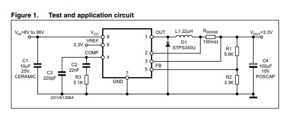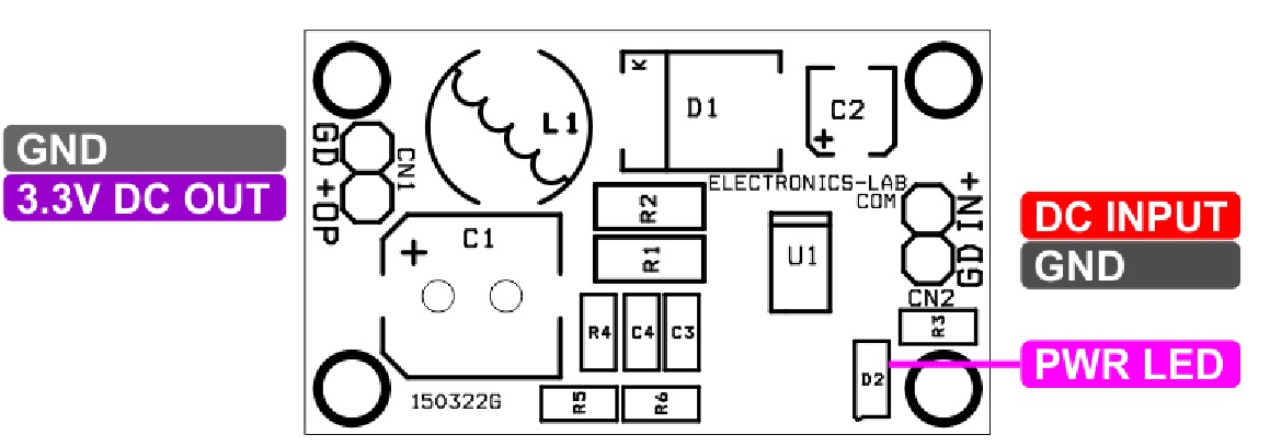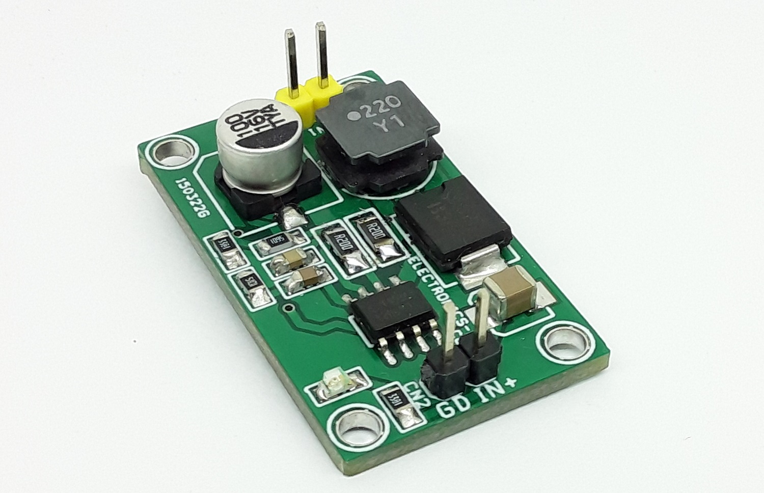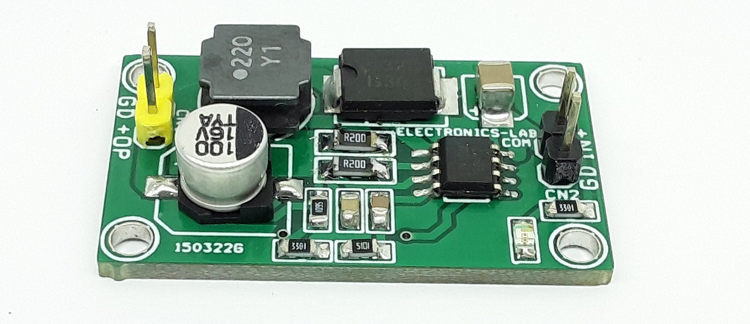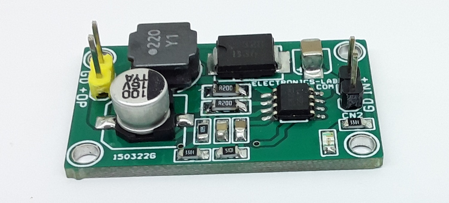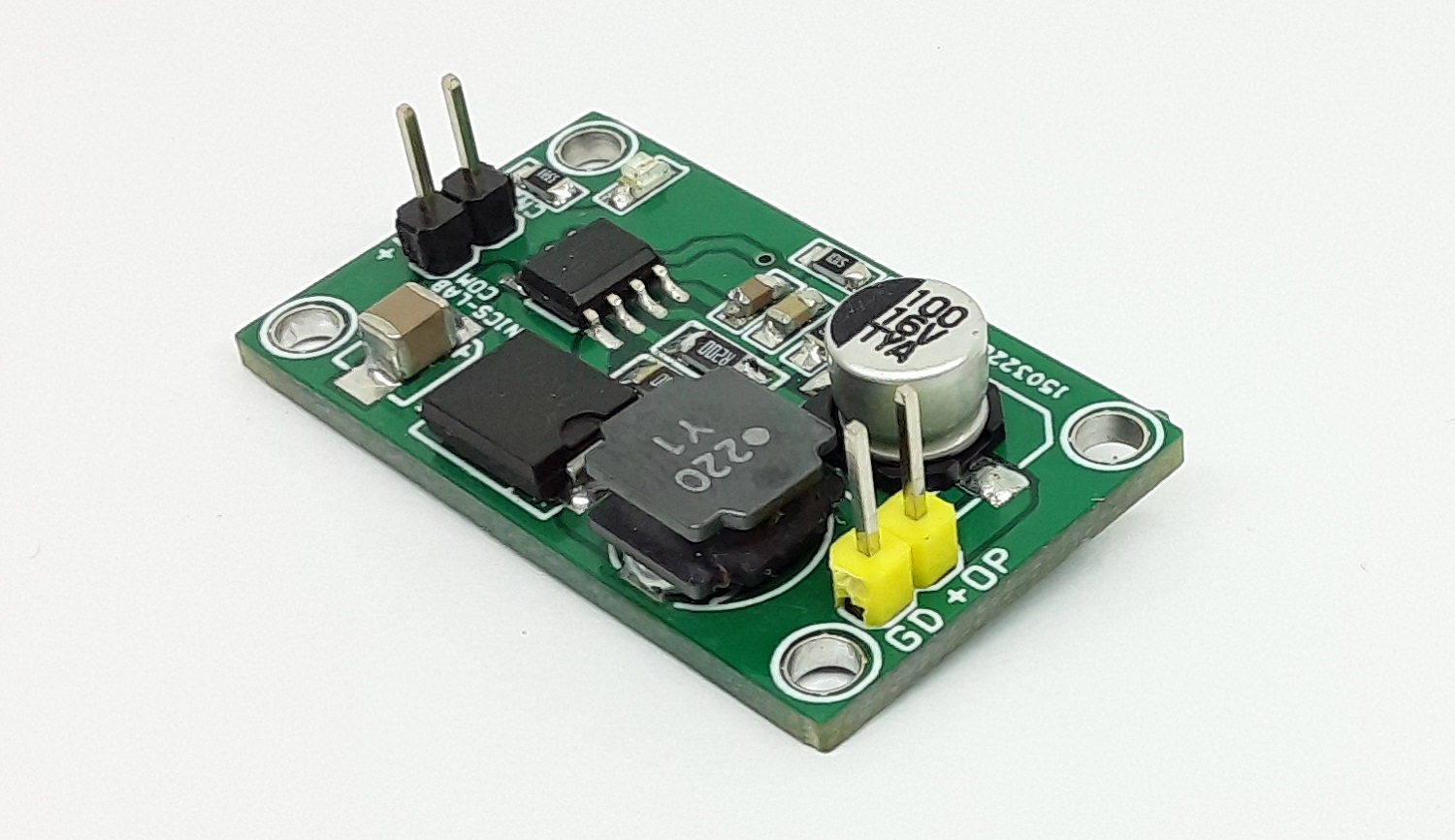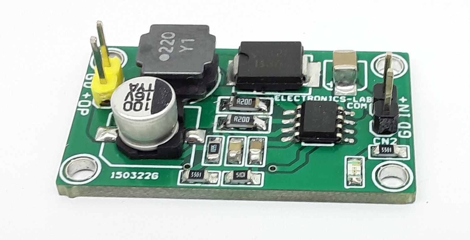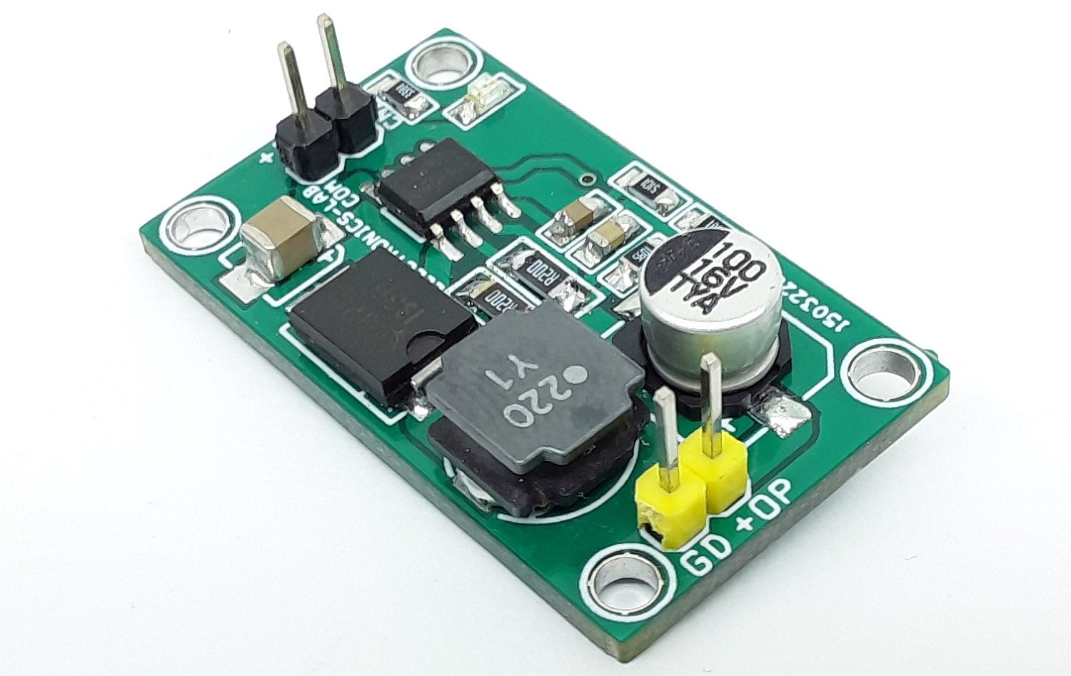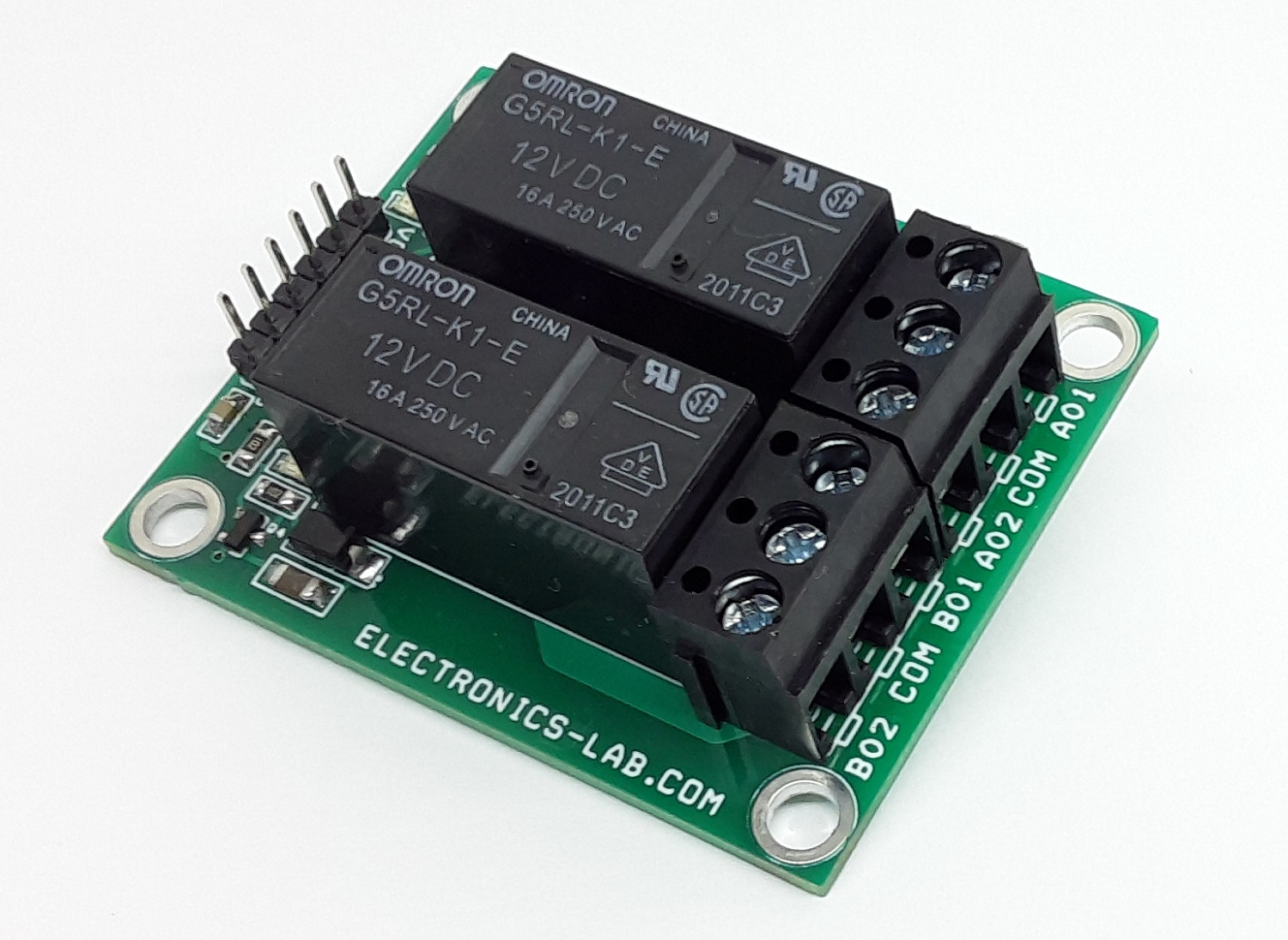
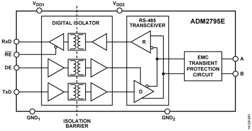
The project presented here is an isolated RS-485 transceiver that features up to ±42 V of ac/dc peak bus overvoltage fault protection on the RS-485 bus pins. The project is based on the ADM2795E chip. The device integrates Analog Devices, Inc., iCoupler® technology to combine a 3-channel isolator, RS-485 transceiver, and IEC electromagnetic compatibility (EMC) transient protection in a single package. The ADM2795E is an RS-485/RS-422 transceiver that integrates IEC 61000-4-5 Level 4 surge protection, allowing up to ±4 kV protection on the RS-485 bus pins (A and B). The device has IEC 61000-4-4 Level 4 EFT protection of up to ±2 kV and IEC 61000-4-2 Level 4 ESD protection on the bus pins, allowing this device to withstand up to ±15 kV on the transceiver interface pins without latching up. This device has an extended common-mode input range of ±25 V to improve data communication reliability in noisy environments. Supports a data rate 2.5Mbps. The board operates with 5V DC, isolated DC-DC converter U1 helps to power the VDD2 supply. D1 is Power LED.
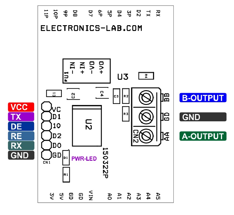
Arduino Pin Connections
- Arduino Digital Pin D1/TX >> TXD – RS484
- Arduino Digital Pin D10 >> DE – RS485
- Arduino Digital Pin D2 >> RE – RS485
- Arduino Digital Pin D0/RX >> RXD – RS485
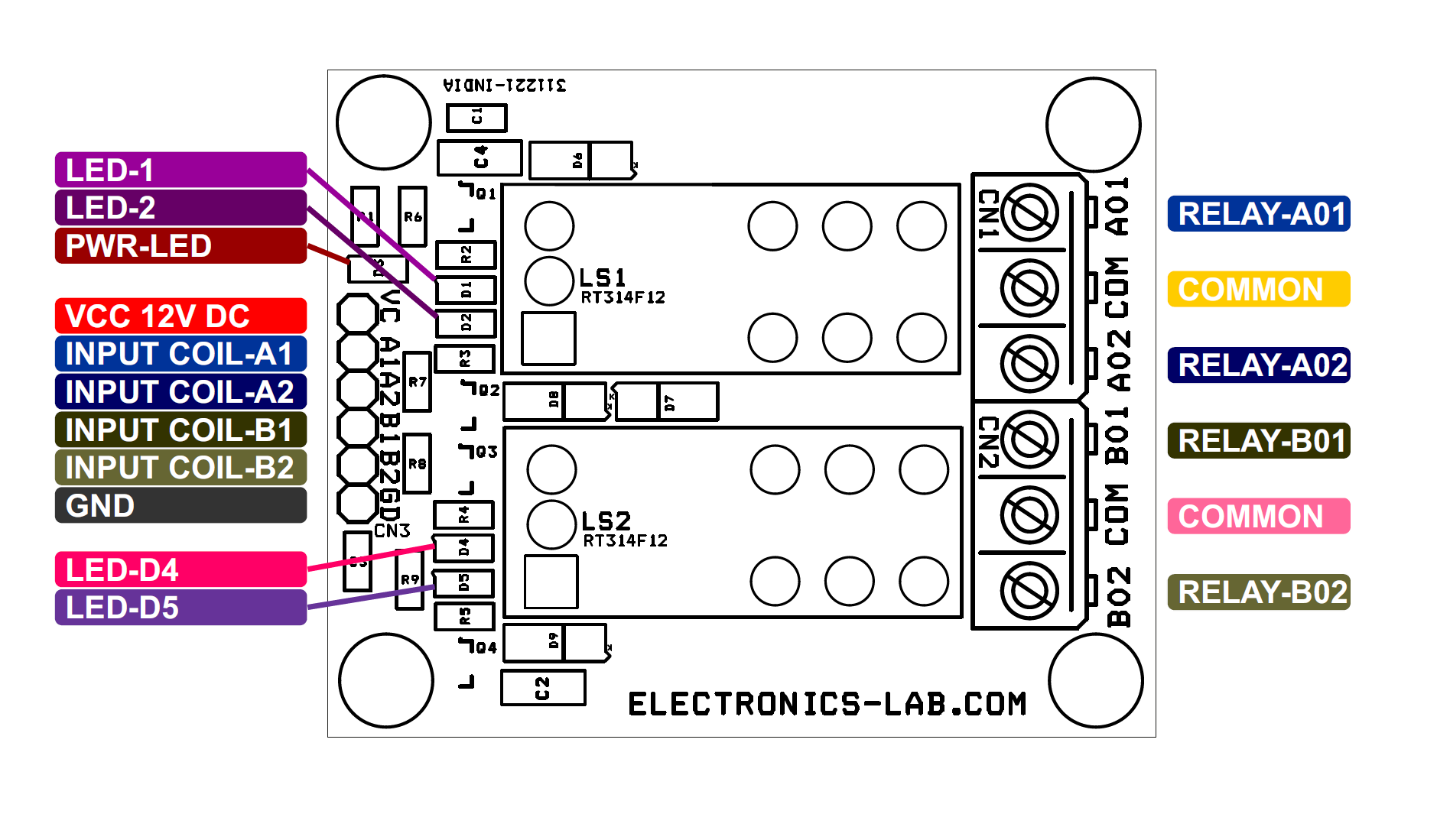
Connection
- CN1 Pin1 = VCC 5V DC
- CN1 Pin 2 TXD
- CN1 Pin 3 DE
- CN1 Pin 4 RE
- CN1 Pin 5 RXD
- CN1 Pin 6 GND
- CN2 Pin 1 RS485 Channel B
- CN2 Pin 2 GND
- CN2 Pin 3 RS485 Channel A
- D1 Power LED
Features
- Power Supply 5V DC
- On Board Isolated DC-DC Converter for single supply operation
- High-Speed Isolated RS485 Communication
- Can be used as Arduino Uno Shield or Standalone Module
- Header Connector for Power Supply and Micro-controller interface
- 3 Pin Screw Terminal for Twisted pair RS485 Connections
- ±42 V ac/dc peak fault protection on RS-485 bus pins
- RS-485 A, B pins human body model (HBM) ESD protection: >±30 kV
- Common-mode input range of −25 V to +25 V
- Receiver short-circuit, open-circuit, and floating input fail-safe
- Supports 256 bus nodes (96 kΩ receiver input impedance)
- On Board Power LED
- PCB Dimensions 50.96 x 35.72mm
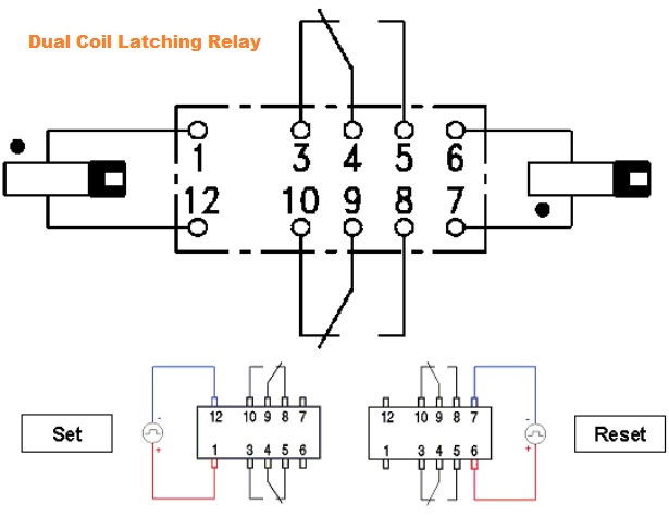
RS-485 Network Biasing and Termination
For a high voltage miswire on the RS-485 A and B bus pins with biasing and termination resistors installed, there is a current path through the biasing network to the ADM2795E power supply pin, VDD2. To protect the ADM2795E in this scenario, the device has an integrated VDD2 protection circuit. The ADM2795E is a fault-protected RS-485 device that also features protection for its power supply pin. This means that the current path through the R2 pull-up resistor does not cause damage to the VDD2 pin, although the pull-up resistor itself can be damaged if not appropriately power rated. The R2 pull-up resistor power rating depends on the miswire voltage and the resistance value. If there is a miswire between the A and B pins, the ADM2795E is protected, but the RT bus termination resistor can be damaged if not appropriately power rated. The RT termination resistor power rating depends on the miswire voltage and the resistance value. Refer data sheet of the chip for more info.
±42 V Miswire Protection
The ADM2795E is protected against high voltage miswire events when it operates on a bus that does not have RS-485 termination or bus biasing resistors installed. A typical miswire event is where a high voltage 24 V ac/dc power supply is connected directly to RS-485 bus pin connectors. The ADM2795E can withstand miswiring faults of up to ±42 V peak on the RS-485 bus pins with respect to GND2 without damage. Miswiring protection is guaranteed on the ADM2795E RS-485 A and B bus pins, and is guaranteed in the case of a hot swap of connectors to the bus pins.
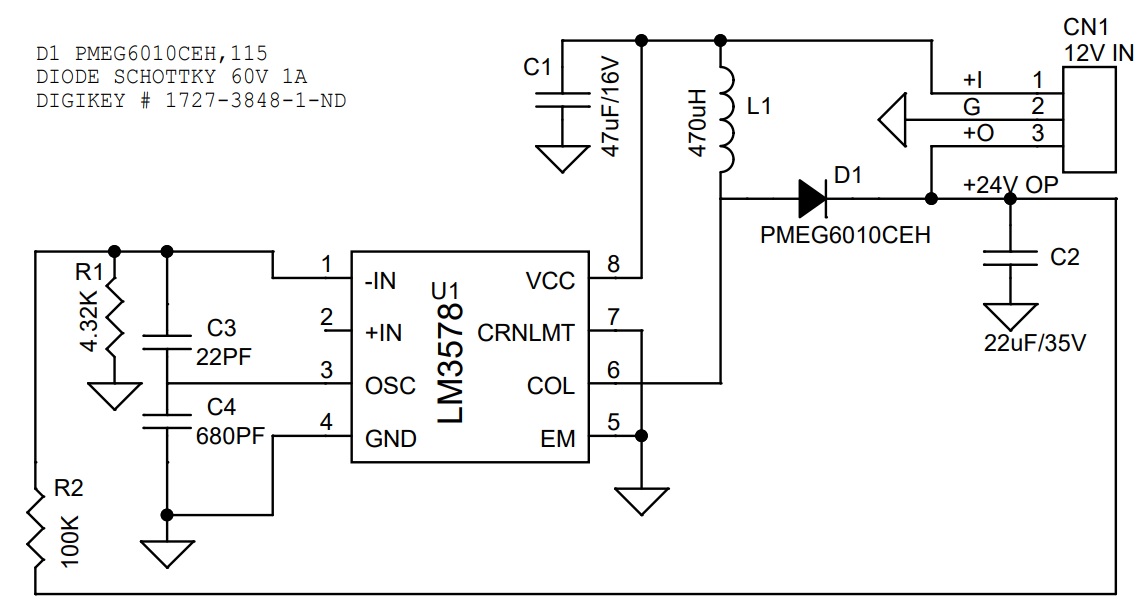
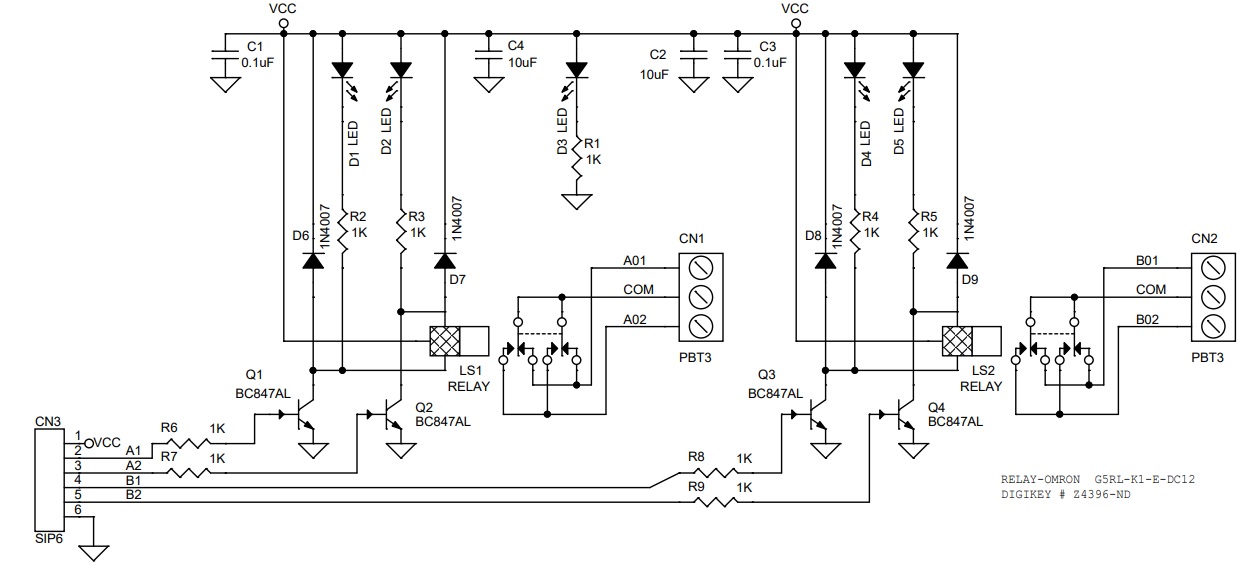
Schematic
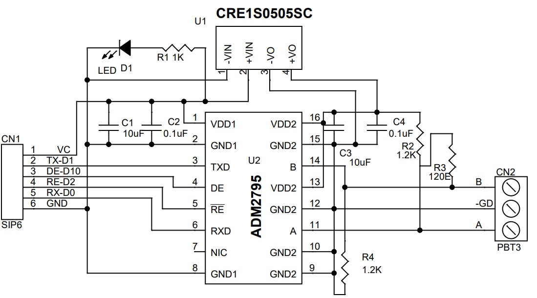
Parts List
| NO | QNTY. | REF. | DESC. | MANUFACTURER | SUPPLIER | PART NO |
|---|---|---|---|---|---|---|
| 1 | 1 | CN1 | 6 PIN MALE HEADER PITCH 2.54MM | WURTH | DIGIKEY | 732-5319-ND |
| 2 | 1 | CN2 | 3 PIN SCREW TERMINAL PITCH 5.08MM | PHOENIX | DIGIKEY | 277-1248-ND |
| 3 | 2 | C1,C3 | 10uF/16V SMD SIZE 1210 OR 1206 | MURATA/YAGEO | DIGIKEY | |
| 4 | 2 | C2,C4 | 0.1uF/50V SMD SIZE 0805 | MURATA/YAGEO | DIGIKEY | |
| 5 | 1 | D1 | LED RED SMD SIZE 0805 | LITE ON INC | DIGIKEY | 160-1427-1-ND |
| 6 | 1 | R1 | 1K 5% SMD SIZE 0805 | MURATA/YAGEO | DIGIKEY | |
| 7 | 2 | R2,R4 | 1.2K 5% SMD SIZE 0805 | MURATA/YAGEO | DIGIKEY | |
| 8 | 1 | R3 | 120E 5% SMD SIZE 0805 | MURATA/YAGEO | DIGIKEY | |
| 9 | 1 | U1 | CRE1S0505SC ISOLATED DC-DC CONVERTER | MURATA | DIGIKEY | 811-3196-ND |
| 10 | 1 | U2 | ADM2795 16SOIC | ANALOG | DIGIKEY | ADM2795ETRWZ-EP-R7TR-ND |
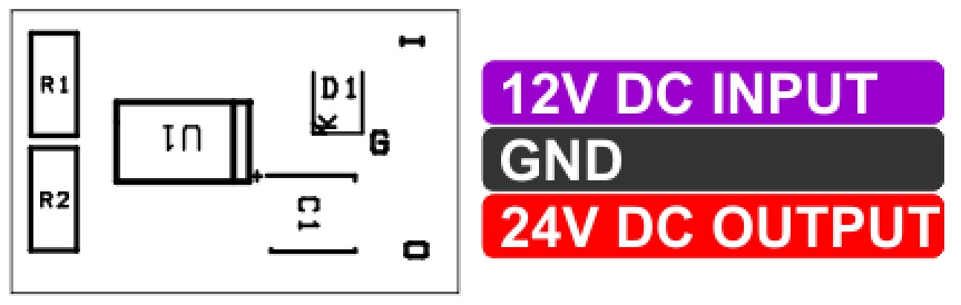
Connections
Block Diagram
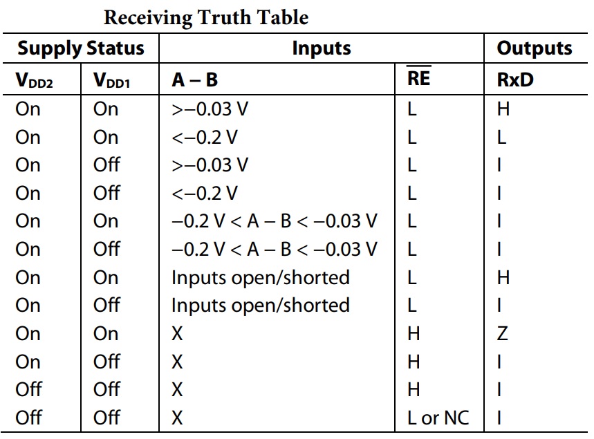
Truth Tables
![]()
Gerber View
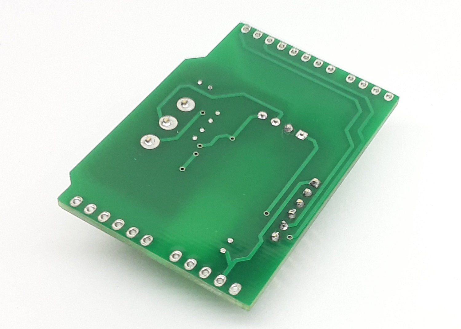
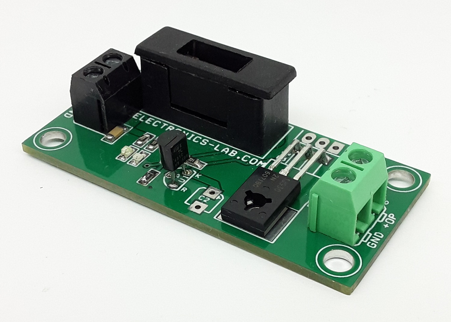
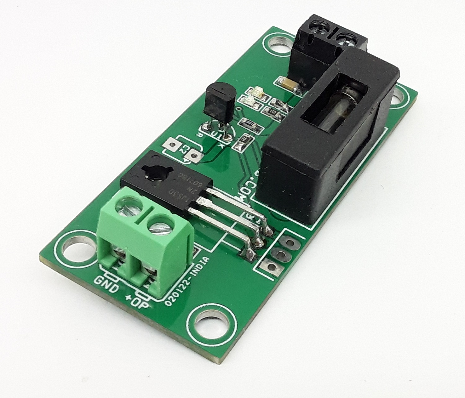
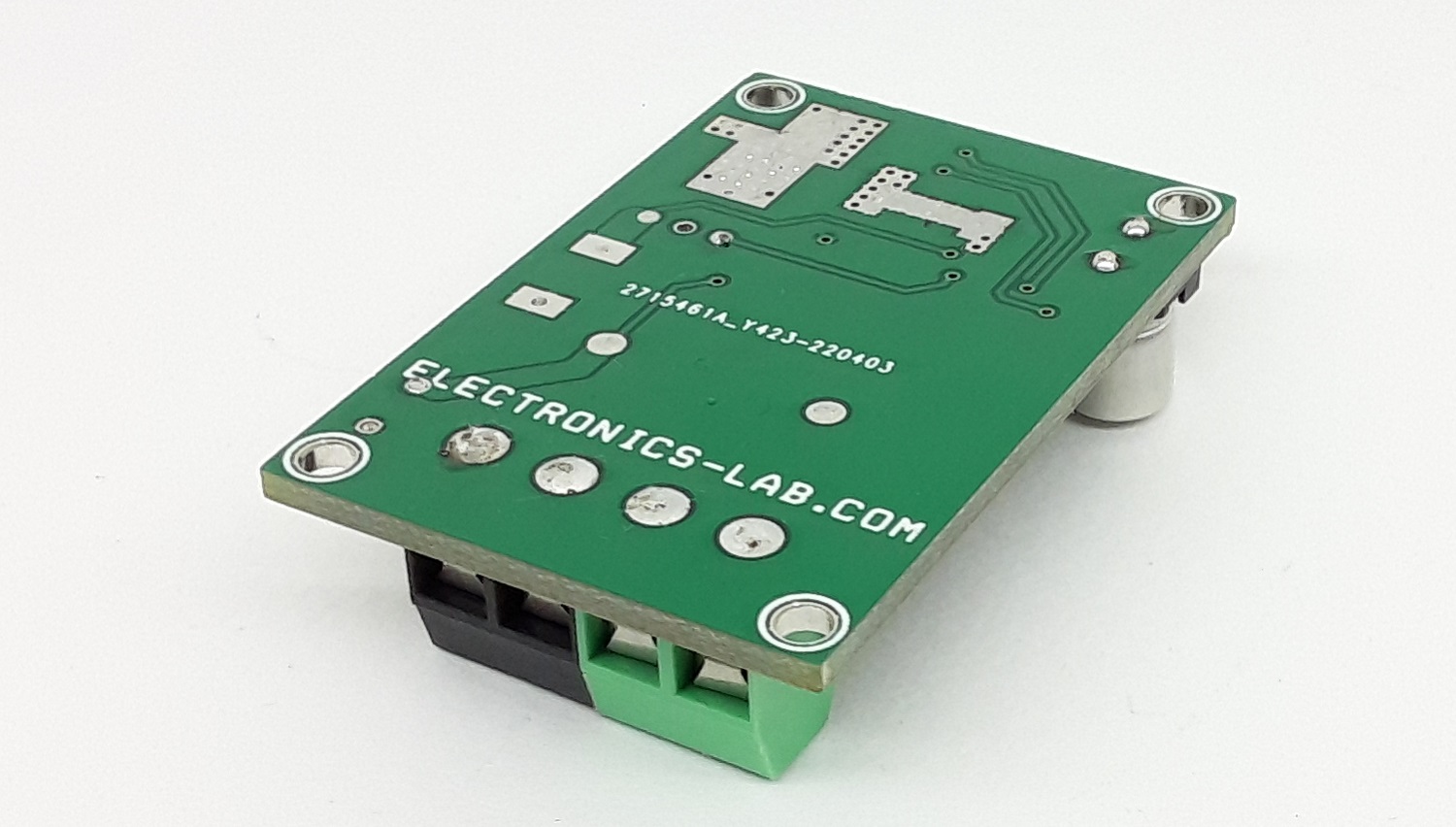
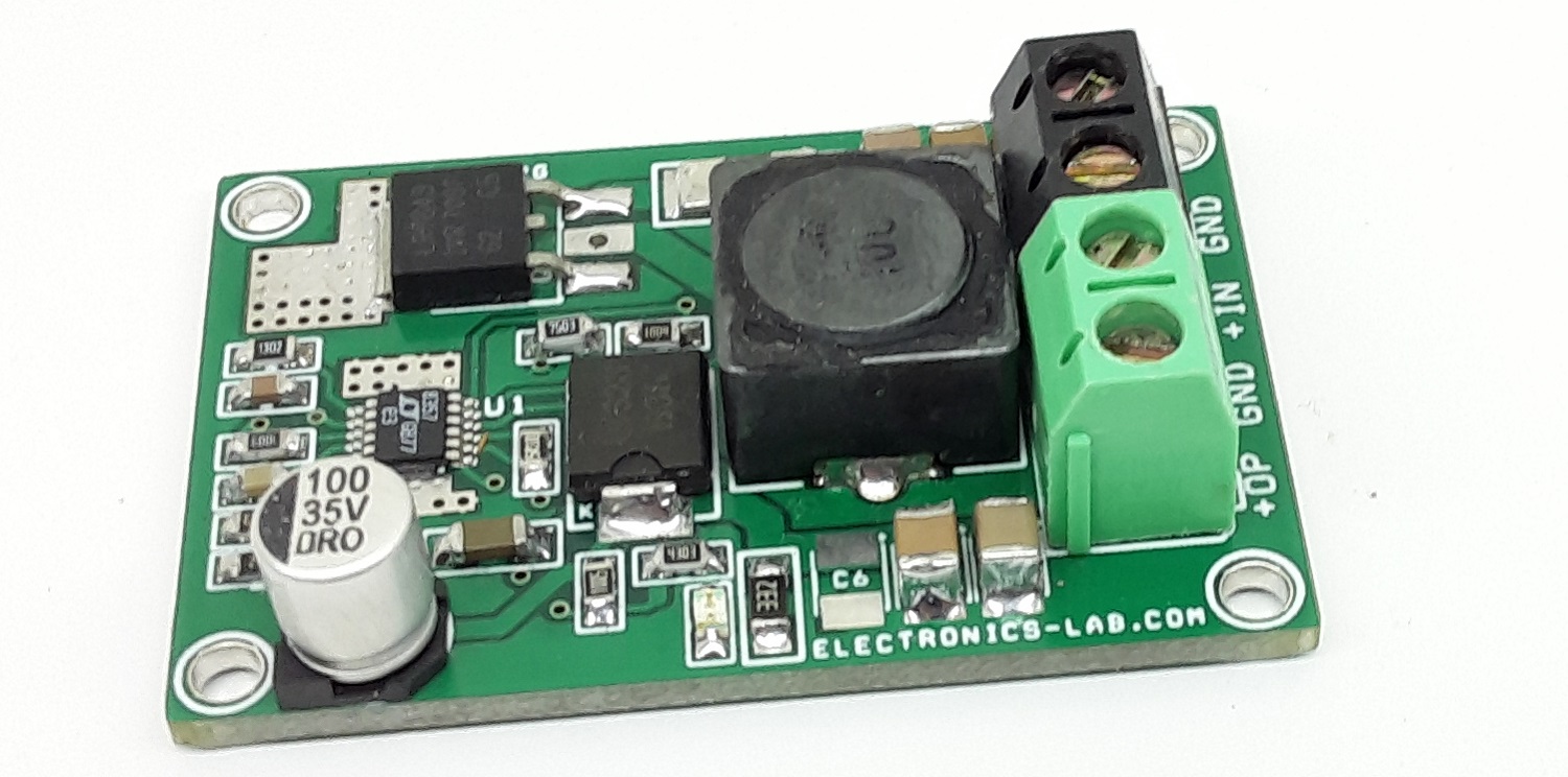
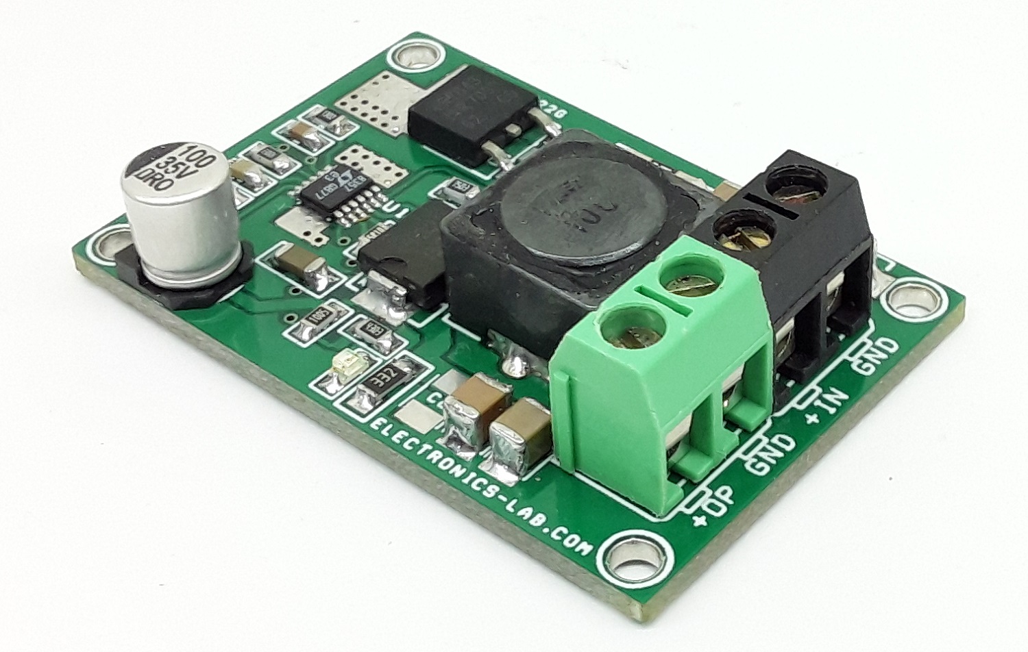
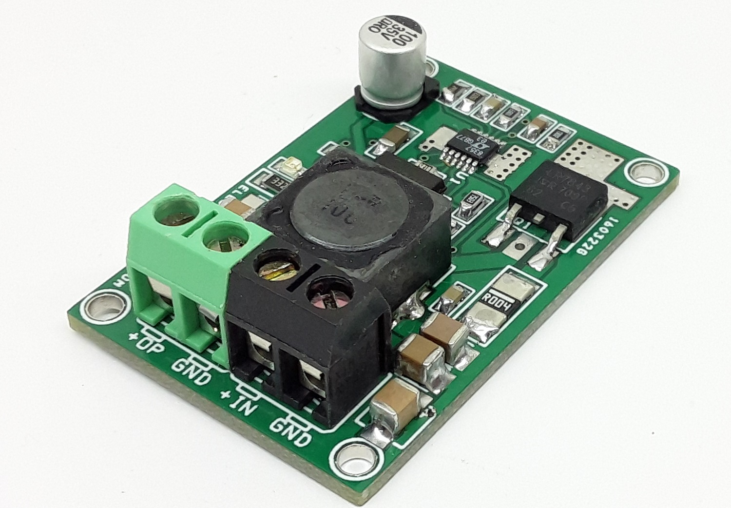
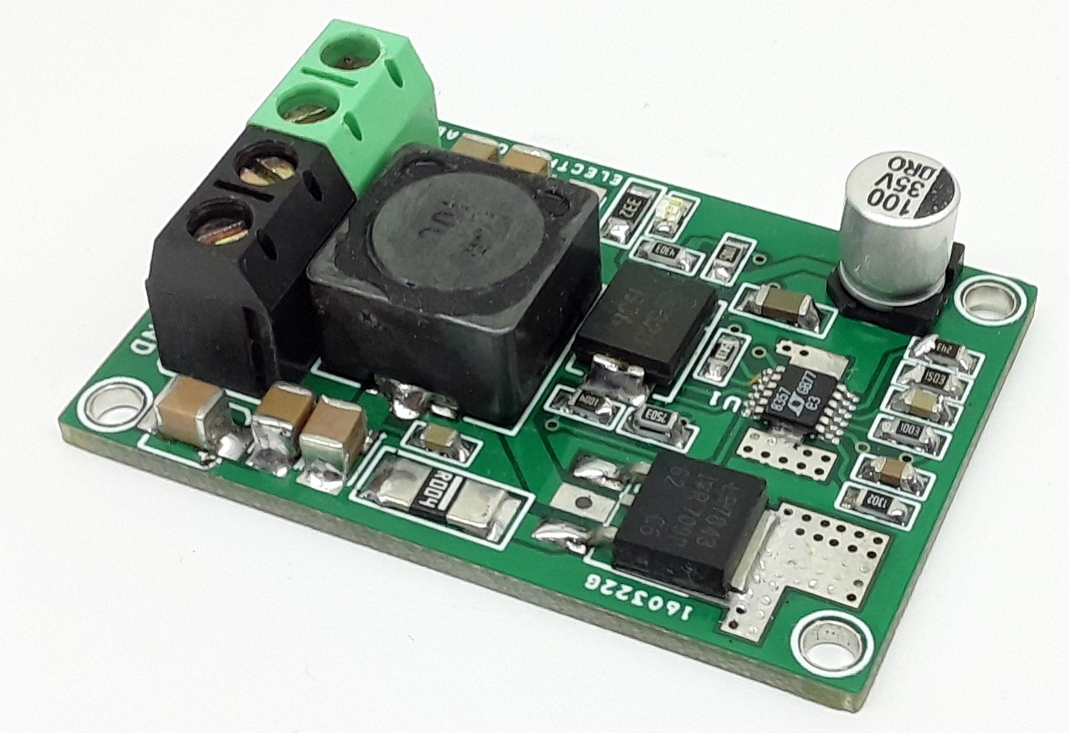
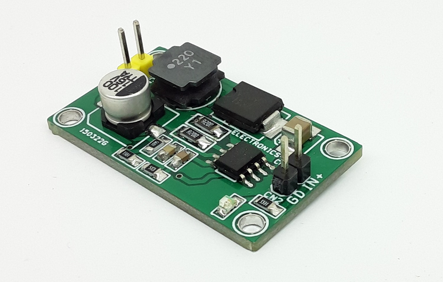
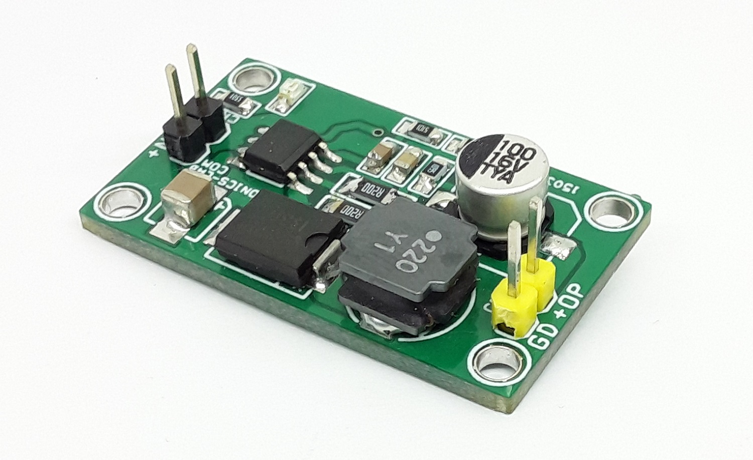
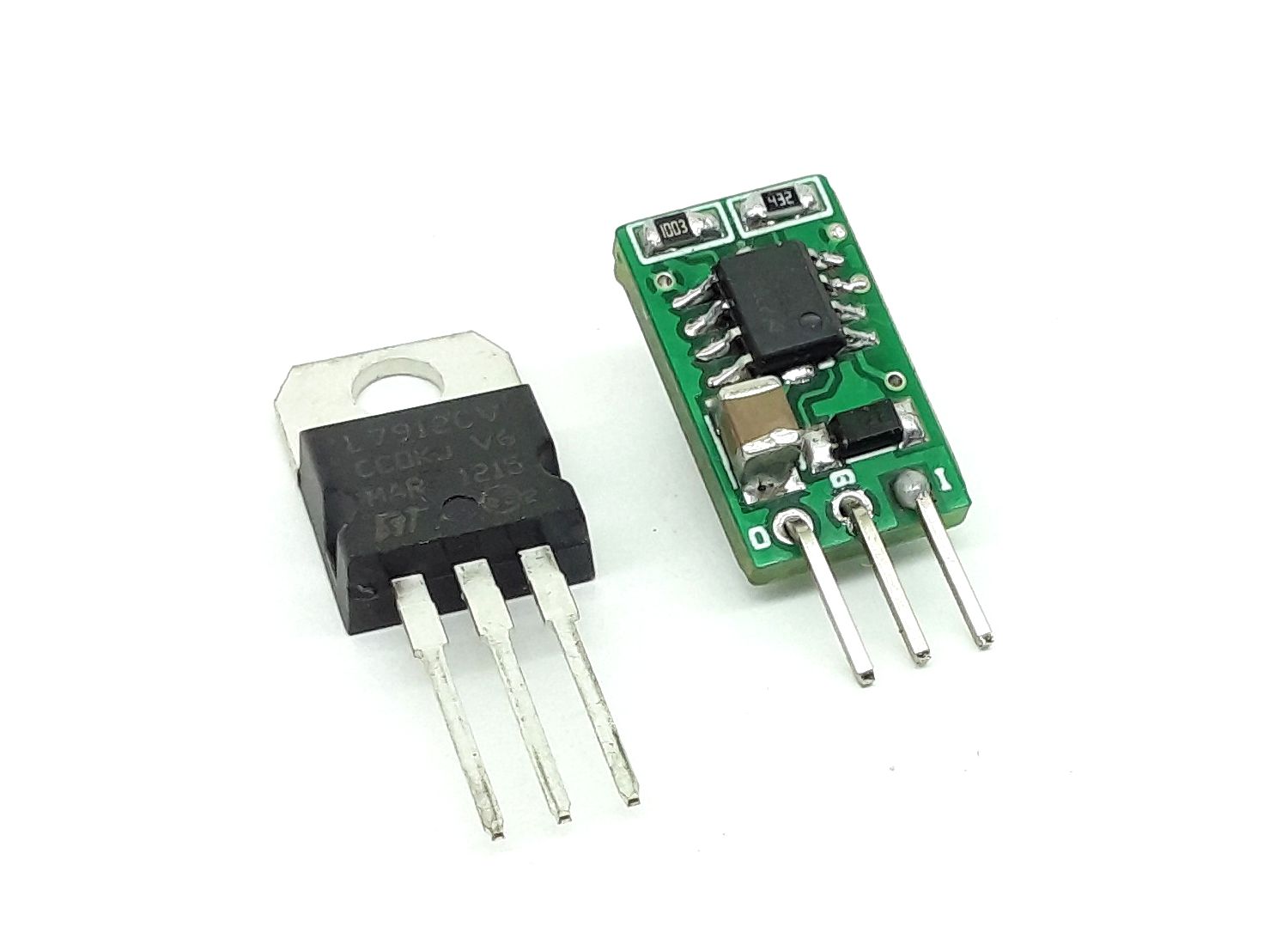
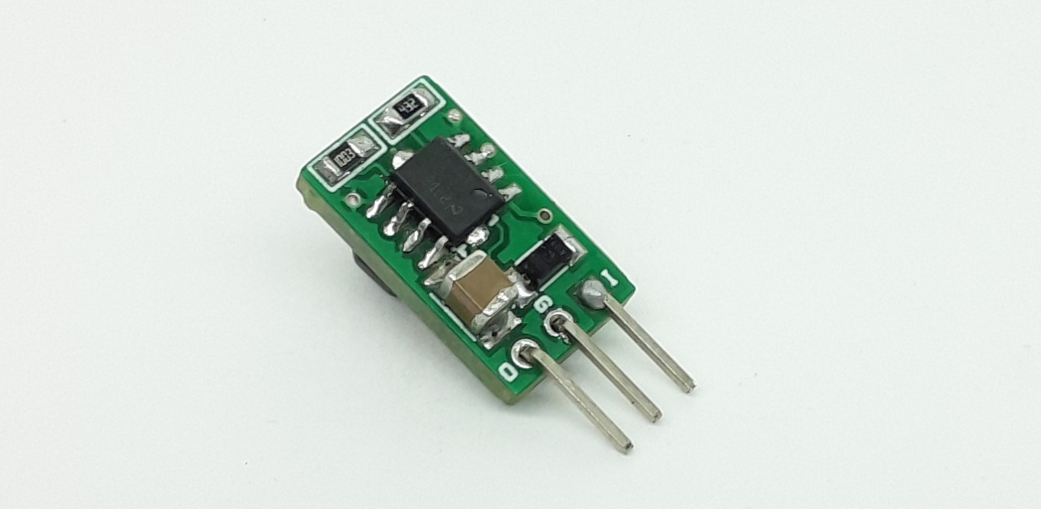
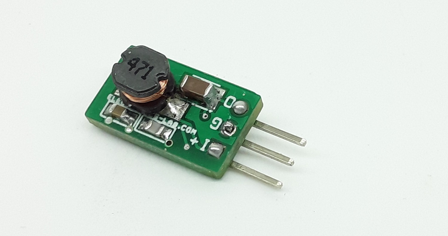
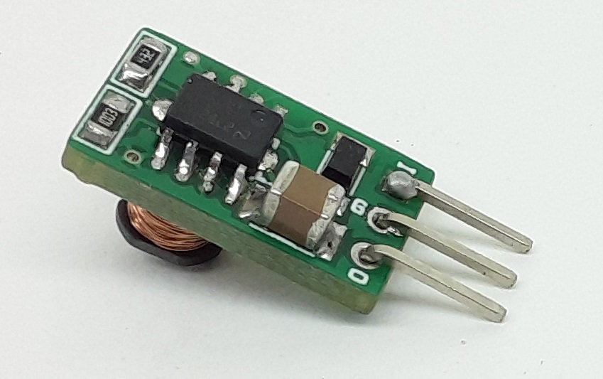
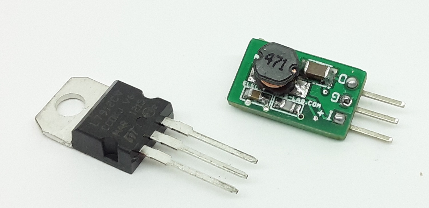
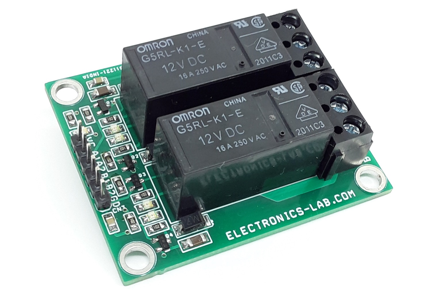
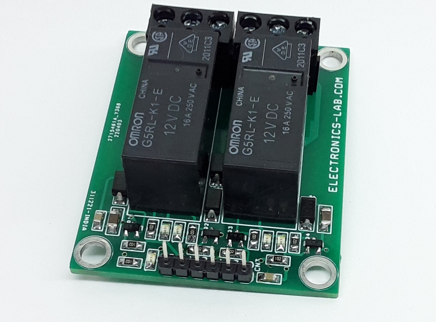
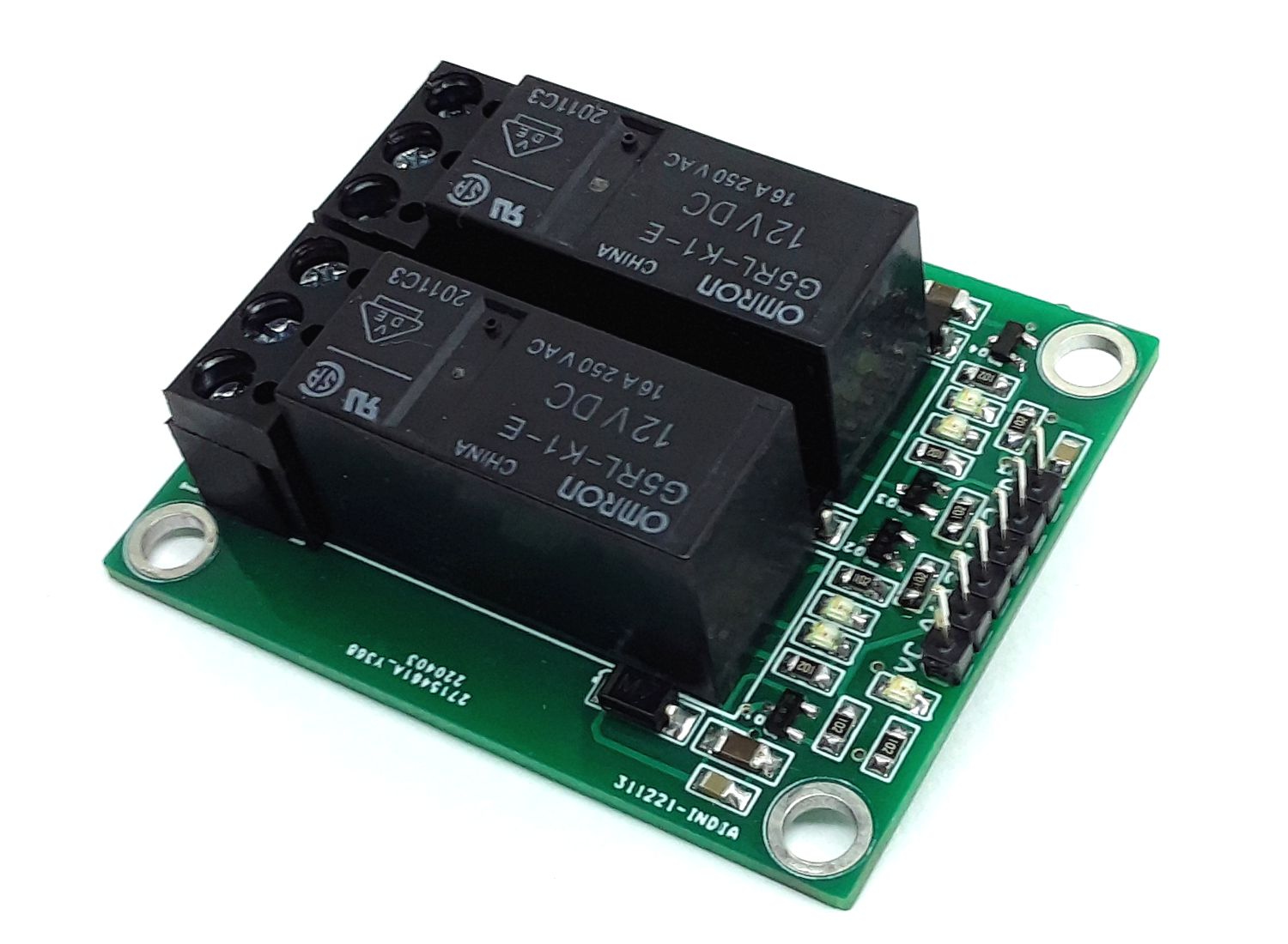
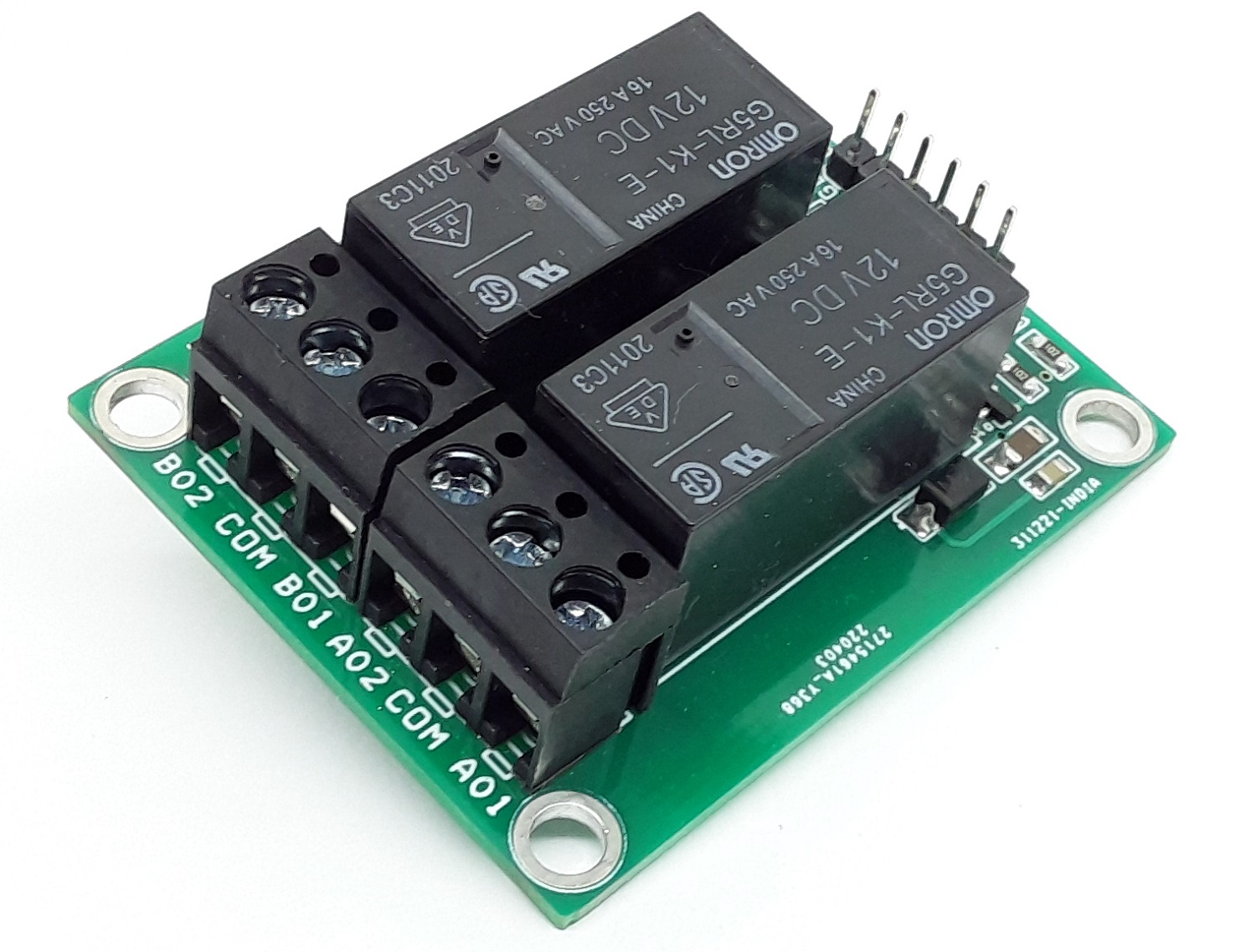
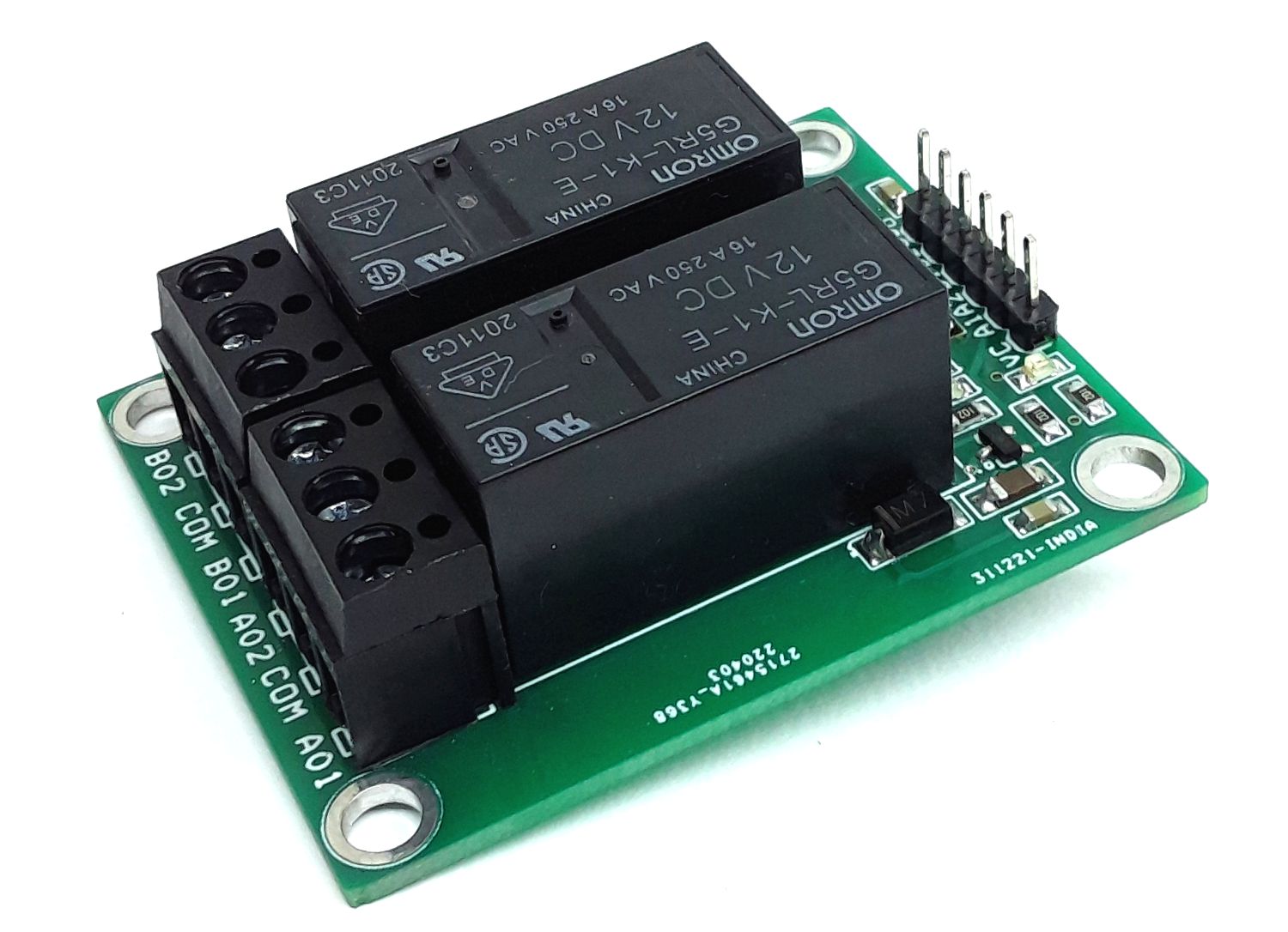
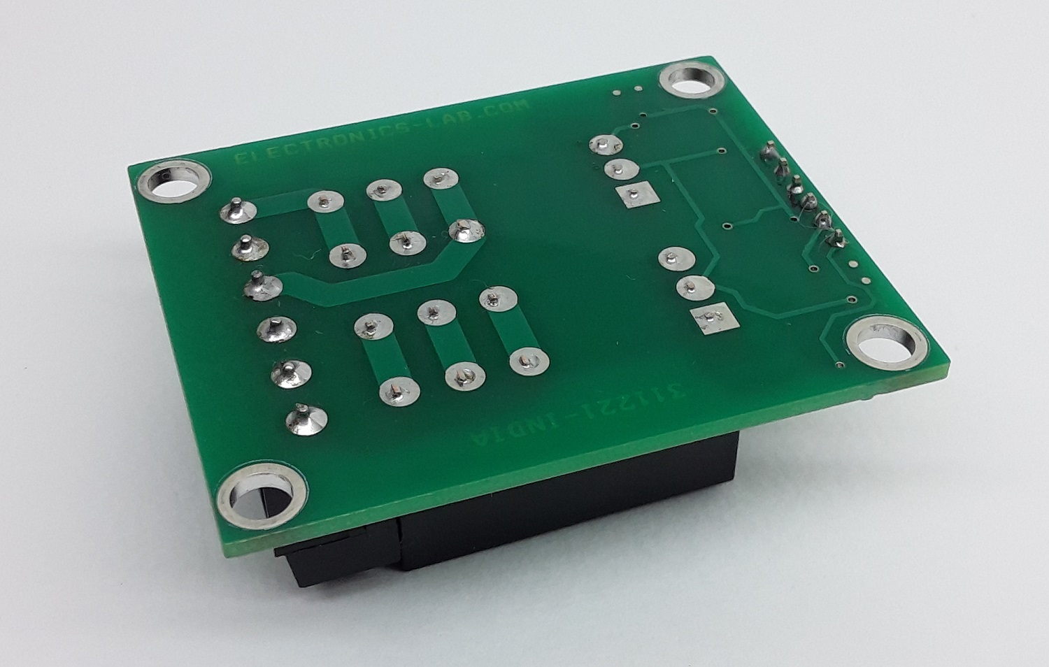
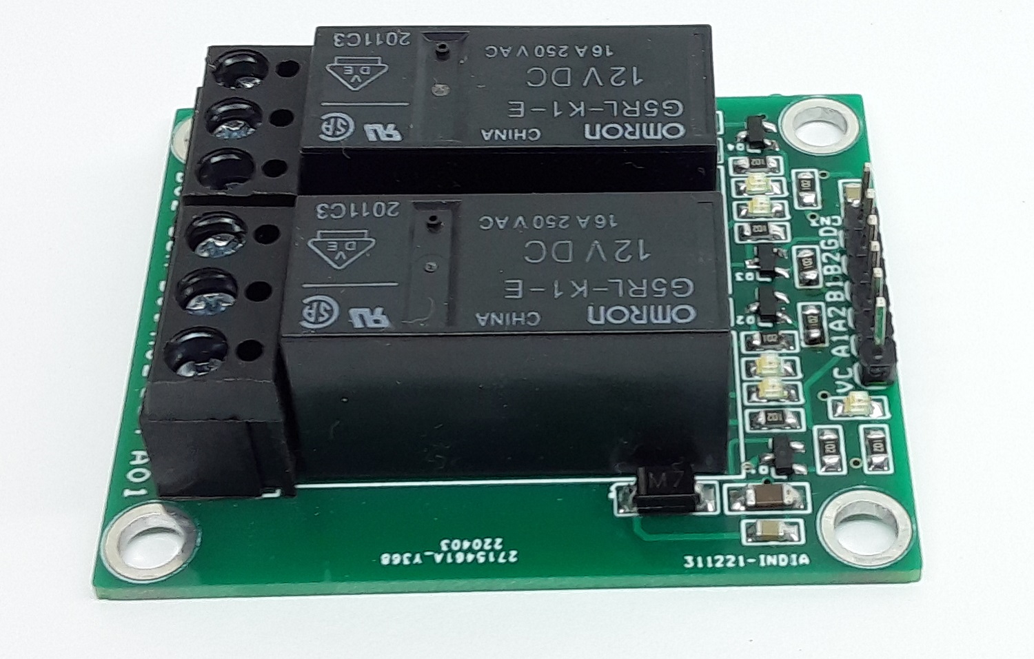
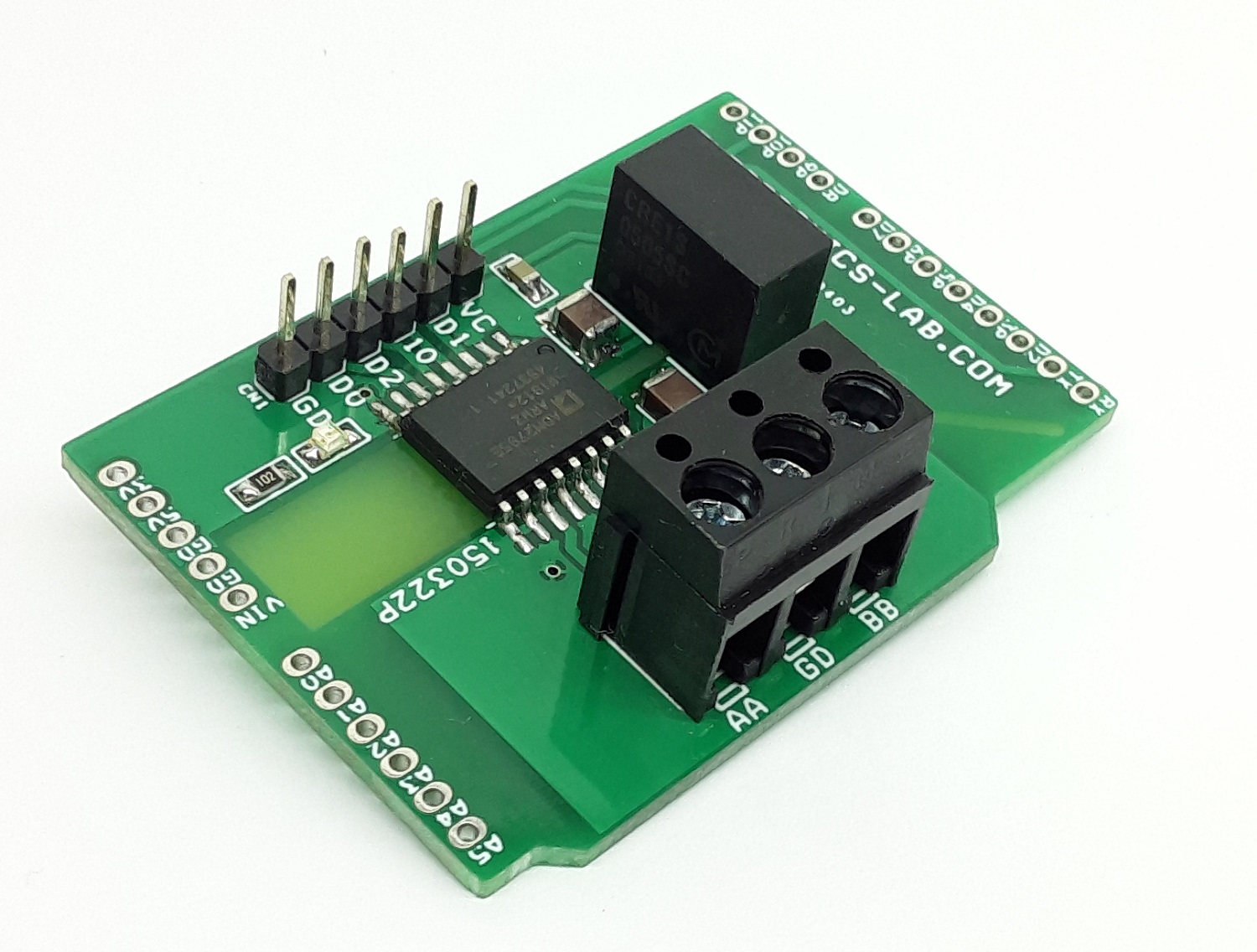
Photos