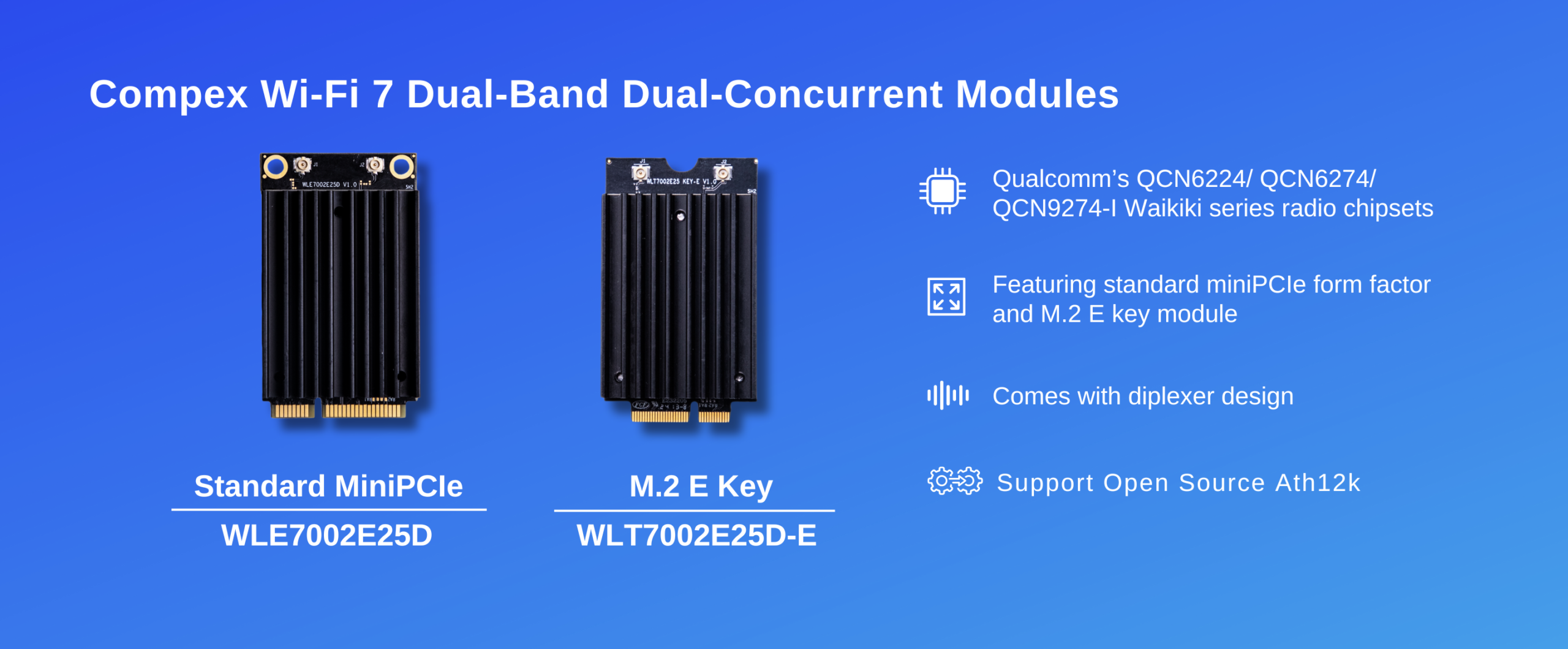
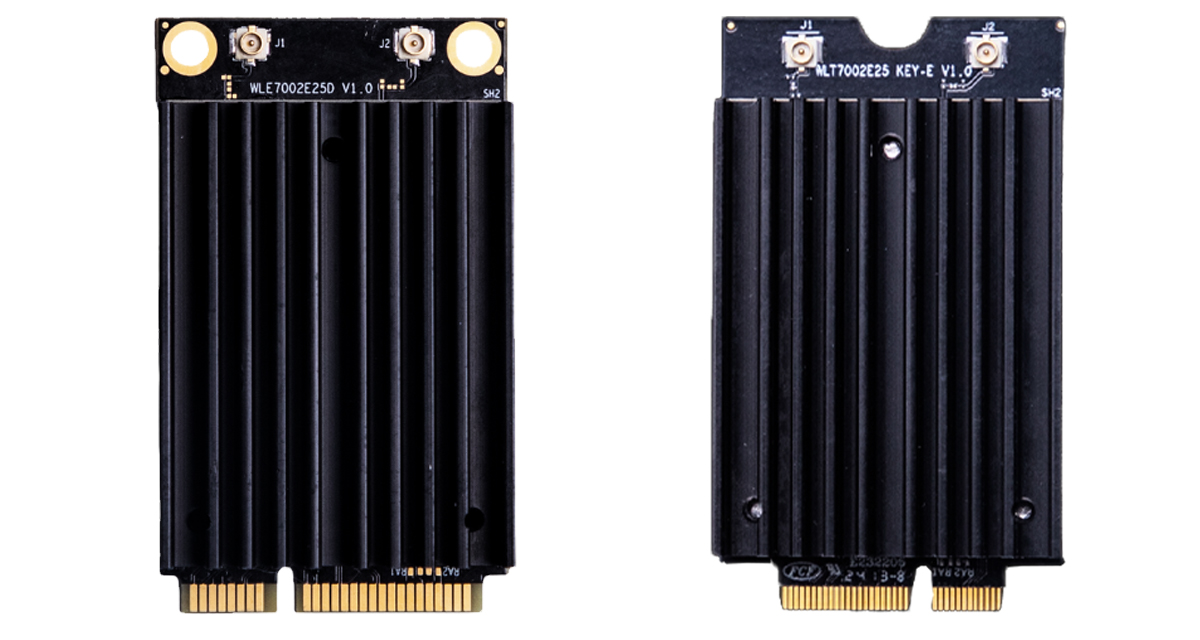
Compex Dual-band Wi-Fi 7 Modules the WLE7002E25D and the WLT7002E25D-E are designed to enhance Wi-Fi reliability by giving you an upgrade from Wi-Fi6 and 6E modules that we have been using for a couple of years now. The WLE7002E25D uses a MiniPCIe form factor, while the WLT7002E25D-E employs an M.2 E-Key interface. Both modules feature Multi-Link Operation to enhance throughput and reliability, advanced OFDMA modulation techniques, and compatibility with Linux operating systems. All these features make this device useful for various applications across enterprise, industrial, cybersecurity, transportation, and small to medium-sized businesses.
Powered by Qualcomm’s QCN6224, QCN6274, and QCN9274-I chipsets, the modules support dual-band operations on 2.4GHz and 5GHz frequencies. Features like Multi-Link Operation enhance throughput and reliability by using multiple frequencies simultaneously. They support advanced OFDMA modulation (BPSK to 4096QAM) and channel widths of 20/40MHz at 2.4GHz and up to 240MHz at 5GHz and are compatible with Linux operating systems for versatile integration. The diplexer design allows a single dual-band antenna to handle both 2.4GHz and 5GHz signals, simplifying device design. Compatibility with the open-source Ath12k driver enables integration with various platforms, including Qualcomm, Marvell, NXP, and x86 systems.
Compex Dual-band Wi-Fi 7 Modules Specifications
Chipset:
Commercial: Qualcomm QCN6224/6274 ‘Waikiki’ series
Industrial: Qualcomm QCN9274-I ‘Waikiki’ series
Interface:
WLE7002E25D: MiniPCIe with PCIe 3.0
WLT7002E25D-E: M.2 E Key with PCIe 3.0
Wireless:
2.4GHz: 2×2 MU-MIMO, up to 688 Mbps (physical data rate)
5GHz: 2×2 MU-MIMO, up to 4324 Mbps (physical data rate)
WLE7002E25D: MiniPCIe interface, designed for general commercial use.
WLT7002E25D-E: M.2 E Key interface, designed for industrial environments with a wider temperature range.
more information about the WLE7002E25D and WLT7002E25D-E can be found on their respective product page, where you can also find the datasheet of the two modules, you can check that out for additional specific details. You can also check out their press release page for some additional details.
The Compex Dual-band Wi-Fi 7 Modules can be purchased for Arrow Electronic where it is priced at around $170.
Electric flux is a measure of how much the electric field vectors penetrate through a given surface.
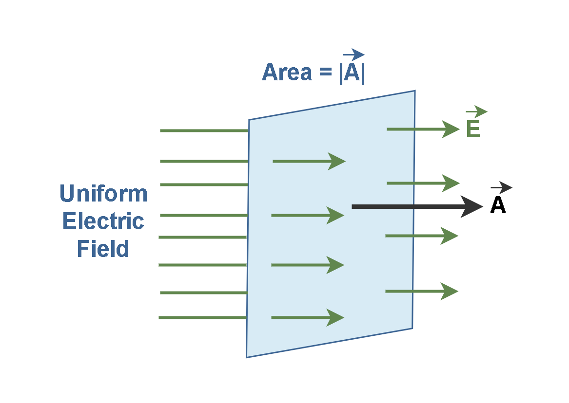
Consider a flat surface with area A in an electric field E that is uniform in both magnitude and direction, as in Figure1. The electric field lines penetrate a surface of area A, which is perpendicular to the field. The normal vector A indicates the position of the plane due to the field lines. The magnitude of the vector |A| is equal to the area of the plane, and the direction of the vector is perpendicular to the surface.
Figure 1: Field lines of E penetrating a plane A
In Figure 1, the number of lines per unit area (N/A) is proportional to the magnitude of the electric field |E|, i.e., |E| ∝ N/|A|. We can rewrite this proportion as N∝|E|.|A|, which means that the number of field lines is proportional to the dot product of E and A. This number is called the electric flux and is generally represented by the symbol ΦEin Equation 1.
Equation 1: The Electric flux due to the electric field E passing through the surface A
Then, electric flux is calculated by a dot product of the electric field and the area normal vector. It is a scalar measure of the flow of electric field lines through an area A oriented perpendicular to the field. Note that ϕE has SI units of Newton-square meters per Coulomb (N.m2/C) and also another unit for electric flux is Volt-meter (V.m). It is called electric flux by analogy with the term flux in fluid flow.
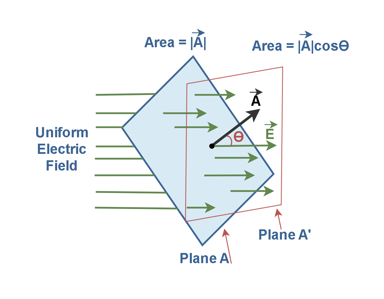
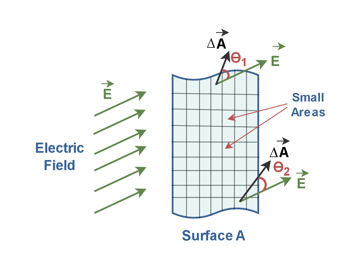
In some cases, the surface under consideration ‘A’ might not be perpendicular to the field E, as depicted in Figure 2.
Figure 2: Field lines of E penetrating a plane A at the angle Ө
In this position, the normal vector A is at an angle Ɵ in respect to the field E lines. We can define a surface with area A’ which is the projection of A and perpendicular to the field E. Based on trigonometric relations, the projection of one area (A) on another area (A’) comes out by multiplying the first area by the Cosine function of the angle between them. Then, the two areas are related by A’ = A cos Ө. Now, we can say the number of lines that cross the area A is equal to the number of ones that cross the projected area A’.
Thus, the expression of the total electric flux for the uniform field E and the flat surface A is explained in Equation 2.
Equation 2: The Electric flux due to the electric field E passing through the surface A’
From Figure 2 and Equation 2, we can conclude that the flux through a surface of fixed area A has the maximum value when the surface is perpendicular to the field (Ө = 0°) and has the minimum value of zero when the surface is parallel to the field (Ө = 90°).
In general, a surface might not be flat, and the electric field may not be uniform (either in magnitude or direction) over the surface. In practice, to find the net flux ϕE through the surface, we can divide up the surface into small sections (square patches) with small areas ∆A (as shown in Figure 3). That could be a good approximation to treat them as the electric field E is reasonably constant in this small area.
Figure 3: Field lines of E penetrating a non-flat surface A at different angles
Then, we find the partial flux at every patch and then add up the results (with the algebraic signs included) to get the net flux, as described by Equation 3.
Equation 3: The net flux due to the electric field E passing through the surface A
However, for non-geometric shapes or closed surfaces, because we do not want to sum hundreds (or more) of partial flux values, we transform the summation into an integral by shrinking the patches from small squares with area ∆A to smaller partial area elements dA. Each infinitesimal element of area dA has a normal direction to its partial area. We use these small area elements as the variables of integration. The total flux then can be calculated by integrating the dot product of two vectors (E . dA) over the total surface, as described by Equation 4.
Equation 4: The net flux due to the electric field E passing through the surface A
Where the electric field is uniform and the surface is flat, the quantity |E| or the product (|E|. cos Ө) is a constant and comes outside the integral. The remaining ∫dA is just an instruction to sum the areas of all the partial elements to get the total area. Note that flux is still a scalar quantity. The small circle on the integral sign indicates that we must integrate over the entire surface, to get the net flux through a closed surface.
In this subject, we are only interested in finding the flux for a special class of surfaces, ones which we call Gaussian surfaces. Such a surface is a closed surface that is, it encloses a particular volume of space and doesn’t have any holes in it. This imaginary surface is used strictly for mathematical calculation, and need not be an actual or physical surface.
The Gaussian surface has a shape determined by the symmetry of the charge distribution. This imaginary surface is chosen so that the electric field is constant everywhere on it. The Gaussian surface can vary in shape and size. It is a closed surface that has an inside and an outside: an example is a sphere.
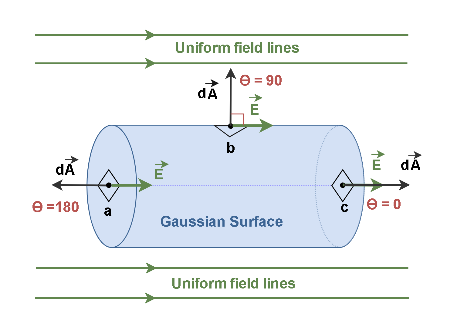
Figure 4 shows a Gaussian surface in the form of a closed cylinder. It lies in a uniform electric field E with the cylinder’s central axis (along the length of the cylinder) parallel to the field. Then, flux might enter on one side and leave on another side.
Figure 4: Field lines of E penetrating a closed Gaussian cylinder
We can find the net flux ΦE with Equation 4 by integrating the dot product (E.dA) over the cylinder’s surface. Recall that this term is converted to (|E|.|dA|.cosӨ) in the calculation. To simplify calculations, we can break up the entire surface into three sections with which we can actually evaluate an integral. Three terms of integration are integrals over the left cylinder cap (section a), the curved cylindrical surface (section b), and the right cap (section c). Equation 5 explains the calculation procedure.
Equation 5: The net flux due to the electric field E passing through the closed Gaussian cylinder
By convention, for a closed surface, the flux lines passing into the interior of the volume are negative and those passing out of the interior of the volume are positive. This convention is equivalent to requiring the normal vector of the surface to point outward when computing the flux through a closed surface. It means the angle Ө between the normal vector and the electric field lines determines the algebraic sign of each term in the calculation. In this way, in section ‘a’ the angle Ө = 180° (then cos Ө = -1), and in section ‘b’ we have Ө = 90° (cos Ө = 0), and for section ‘c’ the angle Ө = 0° (cos Ө = 1).
Let the total area of sections ‘a’ and ‘c’ be A. Substituting the results into Equation 5 leads us to: ΦE= -EA + 0 + EA = 0.
Therefore, the net flux is zero because the field lines that represent the electric field all pass entirely through this Gaussian surface, from the left to the right. It means that there is no charge as the source of the electric field inside the Gaussian cylinder.
Gauss’s Law
Gauss’s law, also known as Gauss’s flux theorem, was developed by the mathematician Karl Friedrich Gauss (1777–1855). It is essentially a technique for calculating the electric field on a closed surface, called a Gaussian surface. Gauss’s law relates the electric flux through a closed surface and the total charge inside that surface.
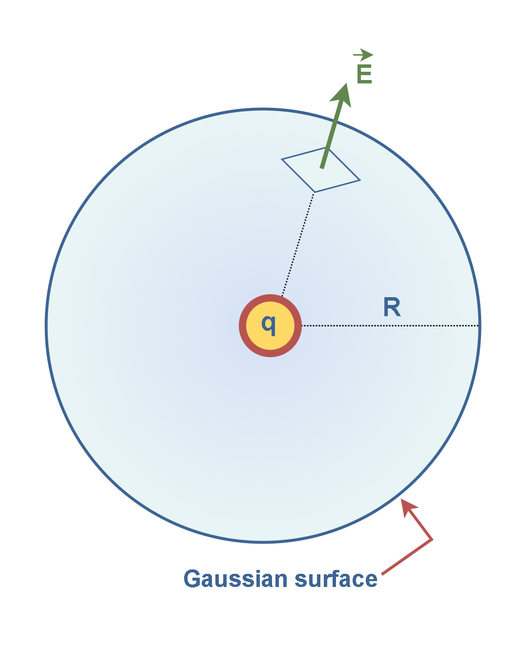
Consider a point charge q surrounded by a spherical Gaussian surface of radius R centered on the charge, as in Figure 5.
Figure 5: The spherical Gaussian surface surrounding a charge q
As we mentioned in previous articles, the magnitude of the electric field everywhere on the surface of the sphere with radius r is calculated by Equation 6.
Equation 6: The electric field E due to the charge inside the sphere of radius R
The constant ε0 is called the permittivity of free space and has the value: ε0 = 8.85 x 10⁻¹² C2/N.m2
Note that the electric field is perpendicular to the spherical surface at all points on the surface. Therefore, the electric flux through the closed spherical surface that surrounds the charge q is (|E|.|A|), where A = 4πR2 is the entire surface area of the sphere. Equation 7 calculates the electric flux.
Equation 7: The flux through a spherical surface surrounding the charge q
Equation 8 gives us the final result:
Equation 8: The flux through a Gaussian surface surrounding a charge q
This result says that the electric flux through a sphere that surrounds a charge q is equal to the charge magnitude divided by the constant ε0. This result can be proven for any arbitrary closed surface that surrounds the charge q.
Suppose we choose a closed surface A in some environment where there are charges and electric fields. We can compute the electric flux ΦEon A. We can also find the total electric charge enclosed by surface A, which we will call Qinside. This leads to the following general result, known as Gauss’s law: ” The electric flux ΦE through any closed surface is equal to the net charge inside the surface, Qinside, divided by ε0“. Equation 9 explains the theorem in mathematical form.
Equation 9: The Gauss’s law for the flux through a closed surface surrounding a charge Qinside
Gauss’s law uses only the component of the electric field that is normal (perpendicular) to the Gaussian surface. This component is mostly denoted by En. In other words, Gauss’s law states that the integral of the normal component of the electric field over any closed surface is proportional to the net charge contained inside that surface.
Equations6 – 9 hold only when the net charge is located in a vacuum or in air (which are the same for most practical purposes). In all the Equations, the net charge Qinside is the algebraic sum of all the enclosed positive and negative charges, and it can be positive, negative, or zero. We include the sign, rather than just use the magnitude of the enclosed charge because the sign tells us something about the net flux through the Gaussian surface: If Qinside is positive, the net flux is outward; if Qinside is negative, the net flux is inward.
The exact form and location of the charges inside the Gaussian surface are also of no concern. The only things that matter on the right side of Equations 6 – 9 are the magnitude and sign of the net enclosed charge. The electric field due to a charge outside the Gaussian surface contributes zero net flux through the surface, because as many field lines due to that charge enter the Gaussian surface as leave it.
Usefulness Of Gauss’s Law
Gauss’s Law is a fundamental principle in electromagnetic theory and it also has several applications in electromagnetism. Gauss’s law is equivalent to Coulomb’s law (which we have already explained in previous articles). But, while Coulomb’s law is formulated in terms of point charges, Gauss’s law is formulated in terms of continuous charge distributions. In such special cases, Gauss’s law is far easier to apply than Coulomb’s law.
We can use Gauss’s Law to find the electric field around charge distributions that have some type of symmetry, but we need to choose Gaussian surfaces of different shapes to take advantage of the symmetry.
There are mostly three kinds of symmetry that work:
Cylindrical symmetry: In cases of line or cylindrical charge distributions, we can make our Gaussian surface a cylinder (see Figure 4, where the charge can be distributed along the axis of the cylinder or over a cylindrical surface inside the blue Gaussian cylinder).
Spherical symmetry: In cases of point charges or spherical distributions, we can make our Gaussian surface a concentric sphere (see Figure 5).
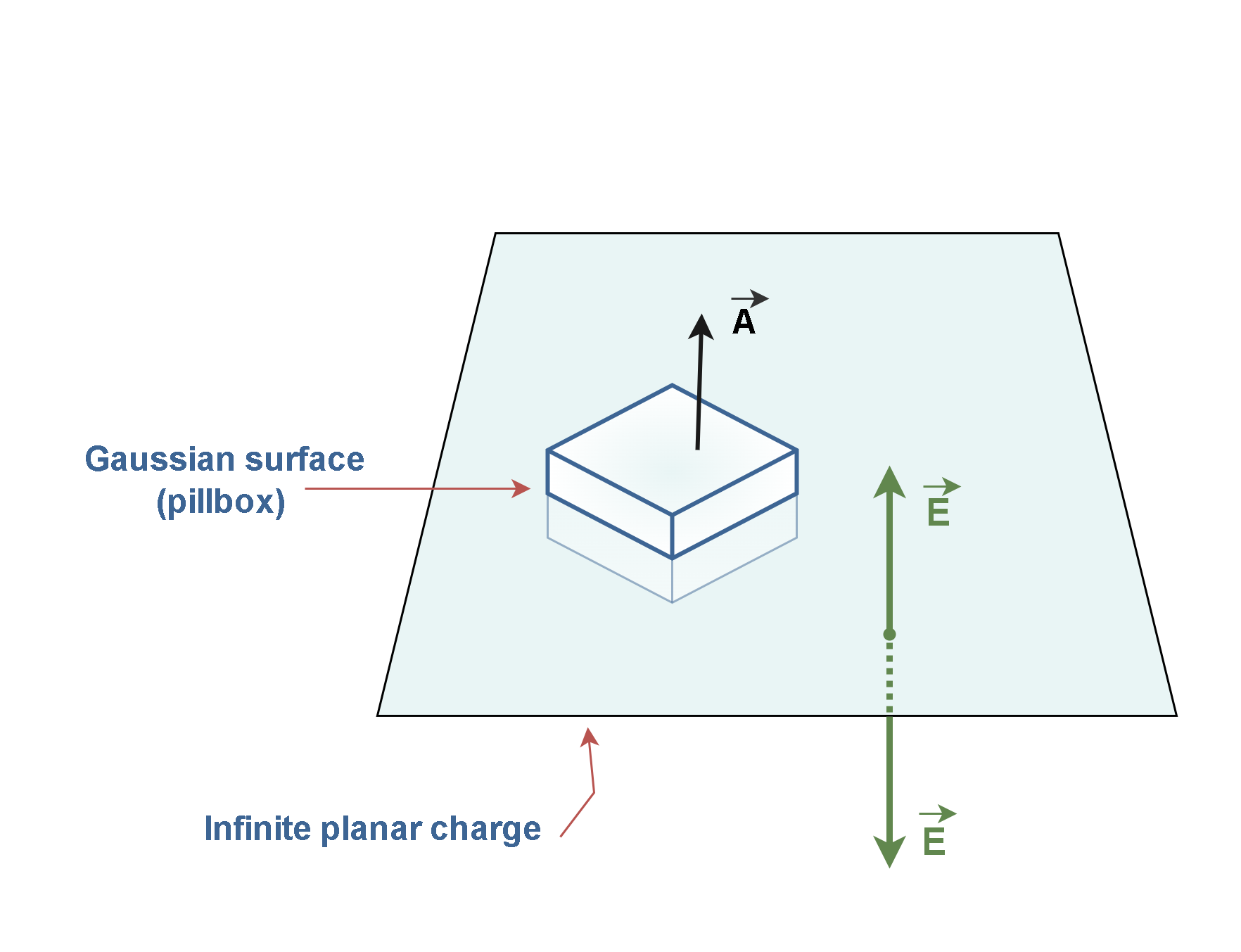
Planar symmetry: In planar charge distributions, we can make a Gaussian “pillbox” that straddles the surface (see Figure 6).
Figure 6: Applying Gauss’s law to an infinite uniform planar charge
Figure 6 demonstrates how Gauss’s law can be applied to determine the electric field strength around an infinite planar charge distribution. In Figure 6, the large flat surface represents an infinite plane of uniform charge. A small box-like shape is the Gaussian surface. Green arrows indicate that the electric field is perpendicular to the plane and equal in magnitude on both sides, but opposite in direction. A black arrow points upward from the top of the pillbox, representing the area vector of the Gaussian surface.
Although cases (2) and (3) technically require infinitely long cylinders and planes extending to infinity, we shall often use them to get approximate answers for “long” cylinders or “large” planes, at points far from the edges.
Finally, even when the charges are not symmetrically distributed, Gauss’s law can still be used to give a rough estimate for design exploration or for checking the result from a computer program.
Summary
The amount of electric field passing through an area oriented perpendicular to the field is defined as the electric flux, ΦE.
ΦE has SI units of N·m²/C (Newton-square meters per Coulomb).
The normal vector with a magnitude equal to the area of a surface indicates the surface position relative to the field lines.
Charges can be surrounded by an imaginary surface, called a Gaussian surface.
Gauss’s law states that the electric flux through a closed surface (a Gaussian surface) is proportional to the charge contained inside the surface.
An inward penetrating field produces negative flux. An outward penetrating field produces positive flux. A field parallel to the surface (skimming) produces zero flux.
Charge outside the Gaussian surface, regardless of its magnitude or proximity, is not included in Gauss’s law calculations.
The field of a uniformly charged spherical surface is identical to that of a point charge located at the center of the sphere with the same total charge.
Gauss’s law may be an easier alternative to Coulomb’s law in some applications.
Gauss’s law combined with symmetry arguments may be sufficient to determine the electric field due to a charge distribution.
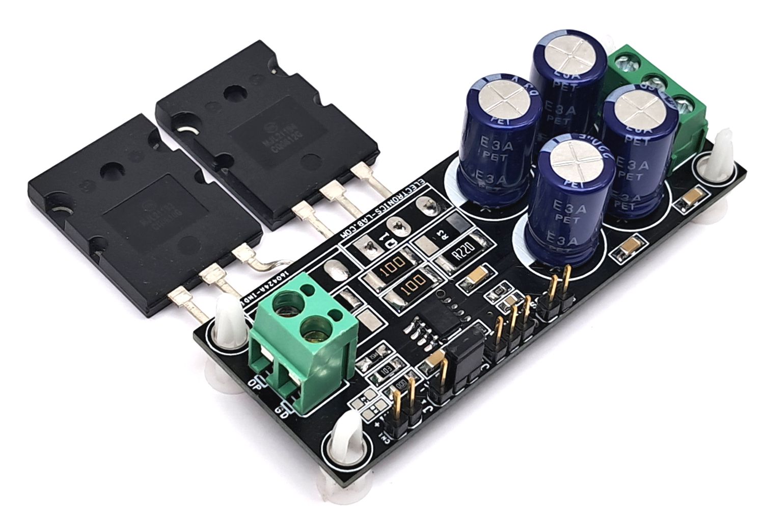
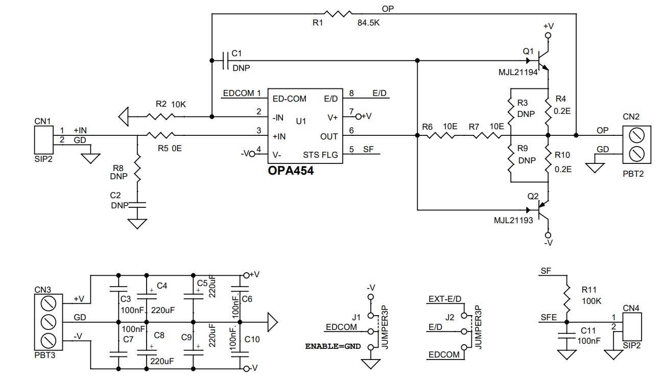
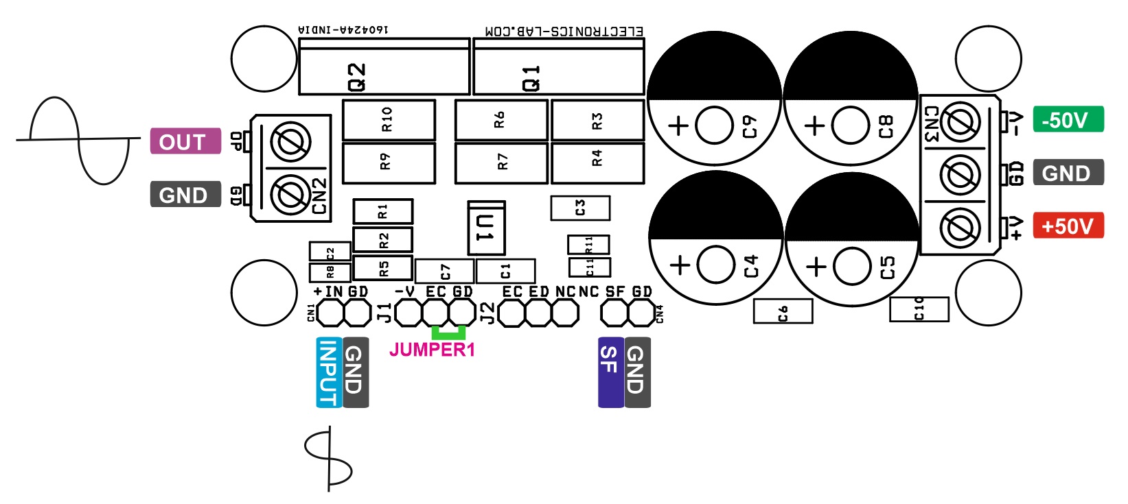
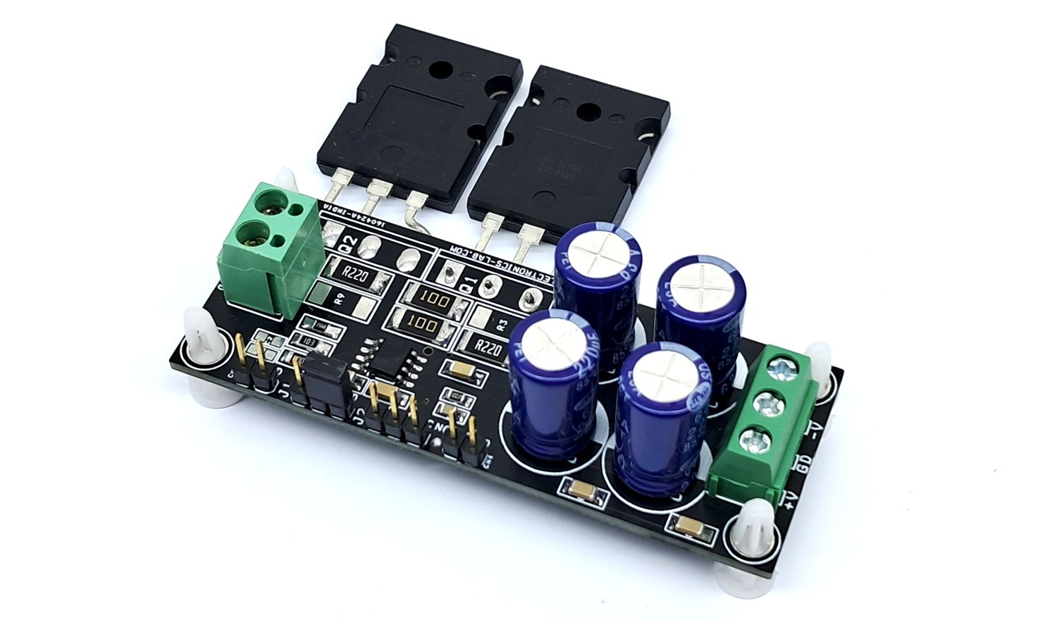
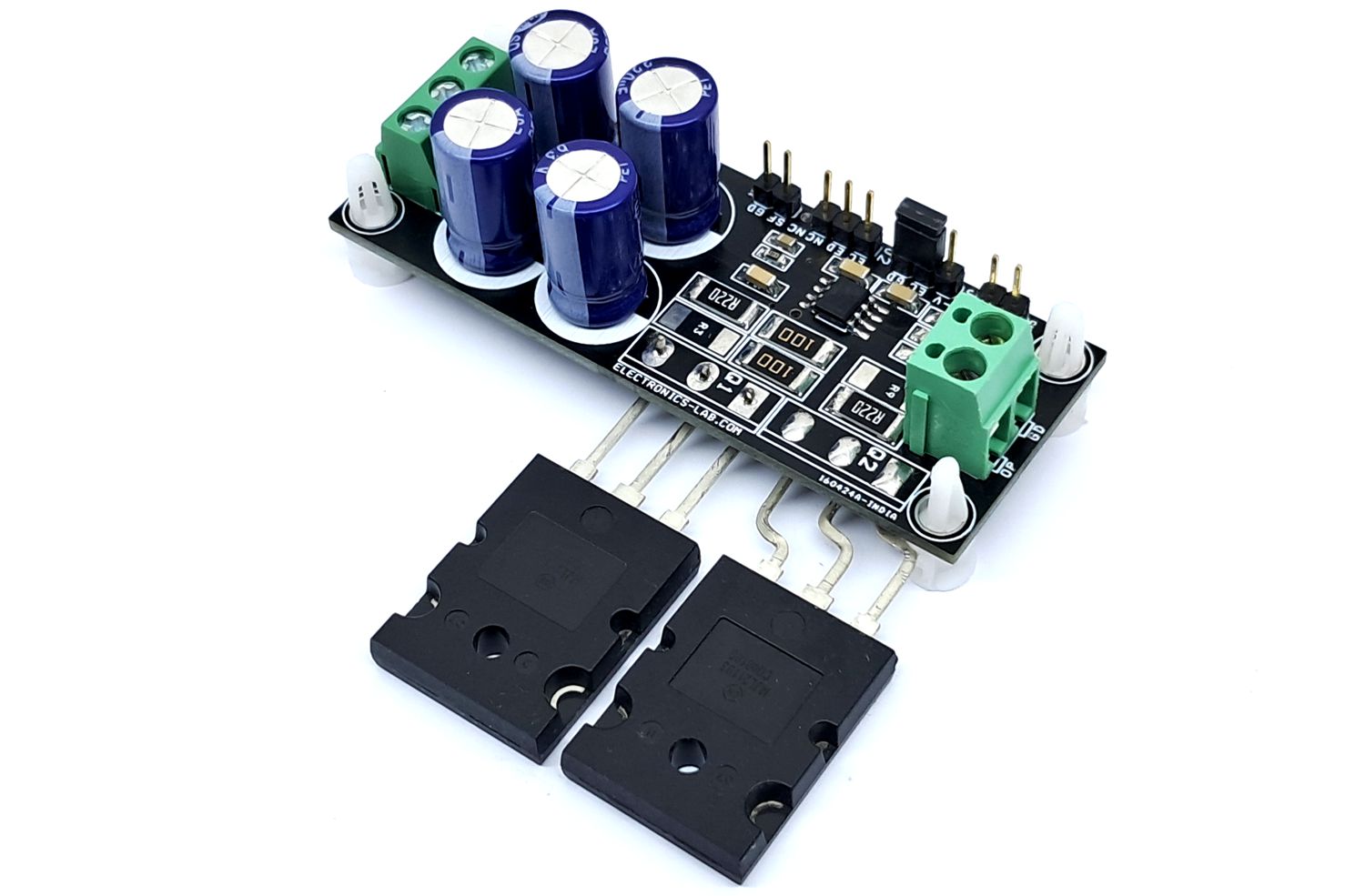
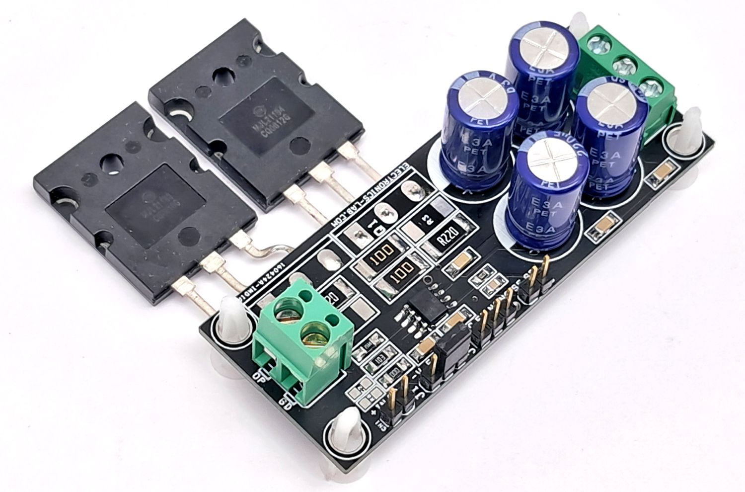
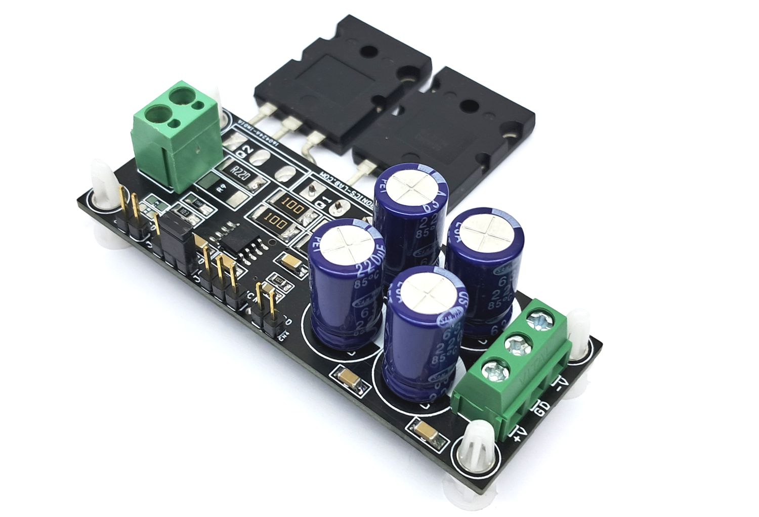
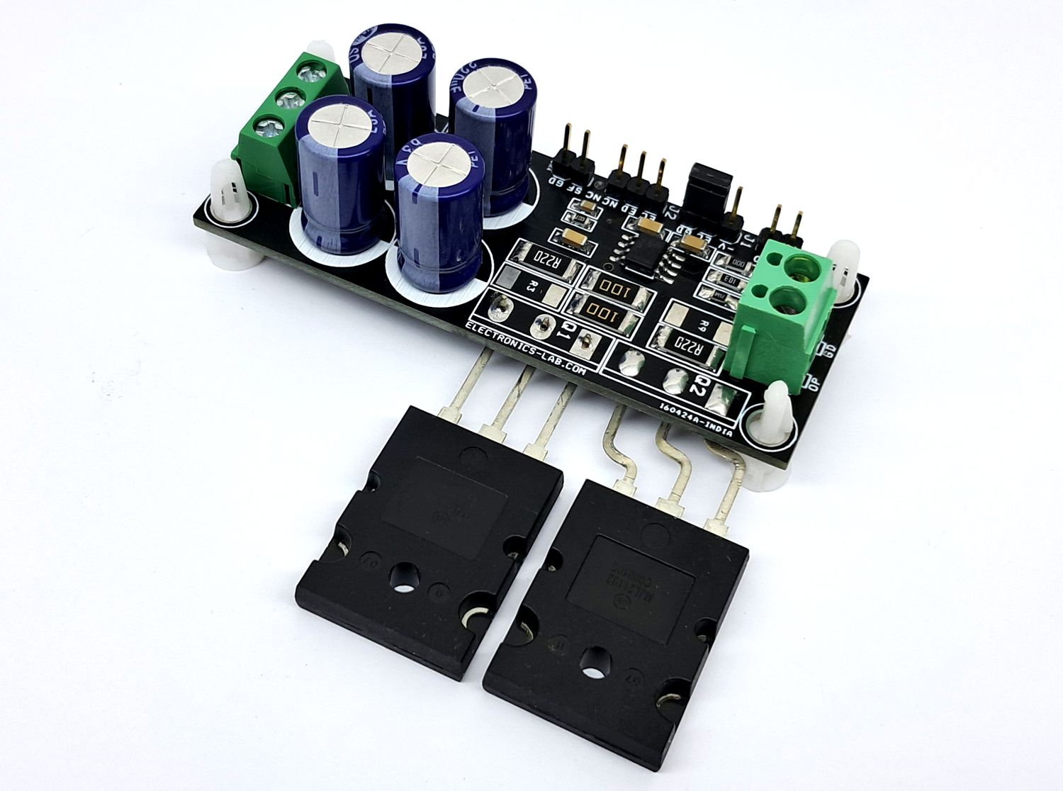
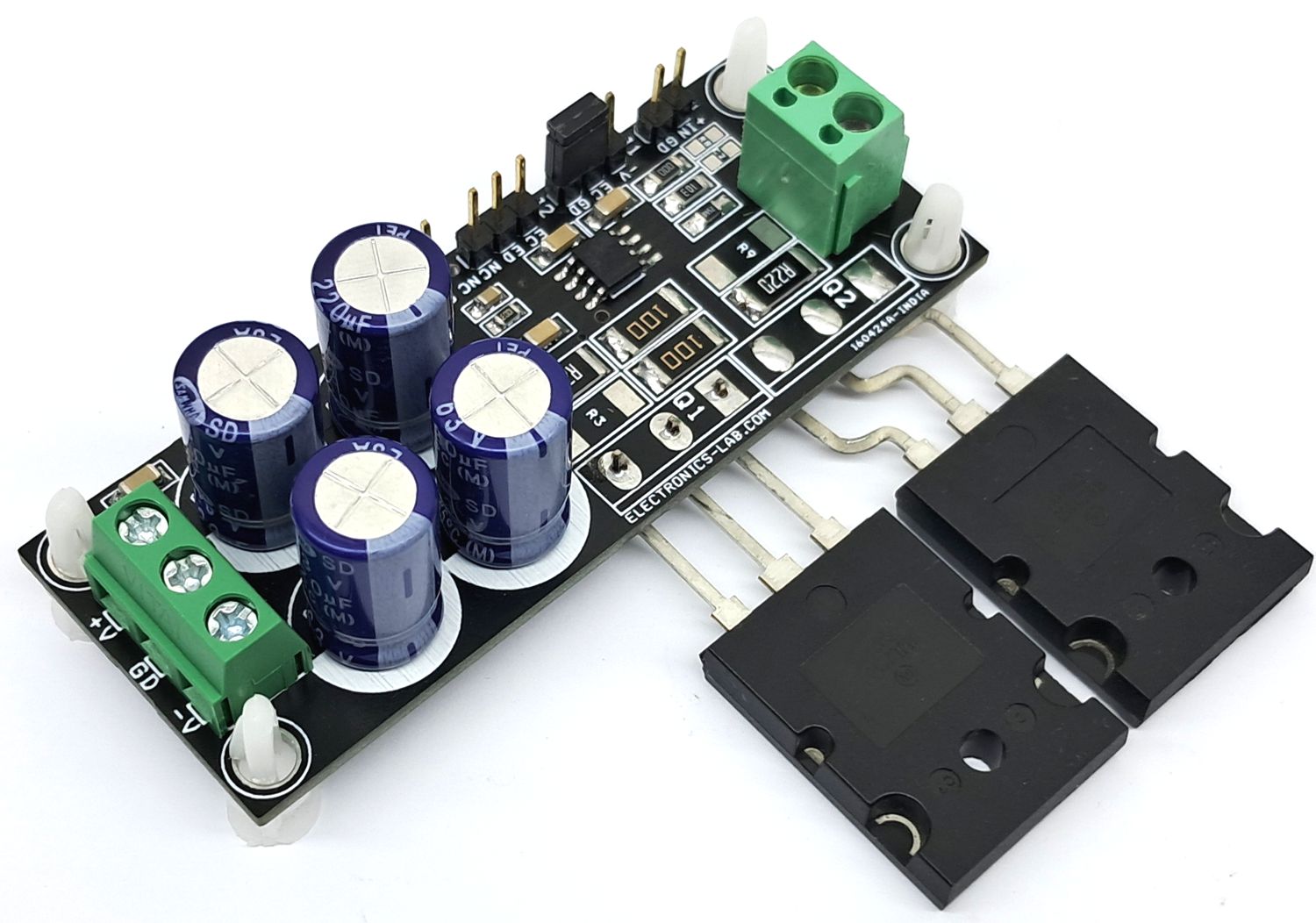
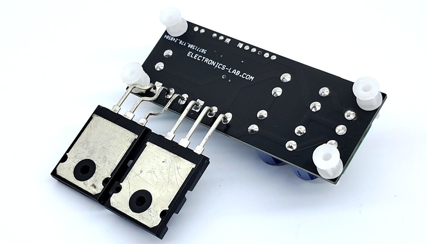
This project provides High Voltage and High Current output swing. The board is built using OPA454OPAMP and 2 x high current NPN/PNP BJT Transistors. Output transistors Q1 and Q2 provide positive and negative output currents to the load. The project works with an input power supply up to +/-50V DC. OPAMP Vout swings from +47V to -48V and OP output swings from +44.1V to -45.1V at 1A. Connect the J1 jumper to GND (EC Middle Pin + GND Pin) to Enable the output.
The output can be independently disabled using the Enable or Disable Pin that has its common return pin to allow easy interface to low-voltage logic circuitry. This disable is accomplished without disturbing the input signal path, not only saving power but also protecting the load.
Test is conducted with Dual +/- 25Vdc Power Source, Load 10/5W Ohms Resistor, Input +/-1V, Output +/-1A Dual 23V DC (Approx.)
SF: The Status Flag is an open-drain active-low output referenced to E/D Com. This pin goes active for either an overcurrent or overtemperature condition.
Features
Power Supply +/-50V DC (Range +/-5V to +/-50V DC)
Output Current Swings 1Amp
Output swings from +44.1 V to –45.1 V at IL = 1 A (Supply Dual 50V)
Input +/-1V
Independent Output Disable or Shutdown
4x4mm Mounting Holes
PCB Dimensions 76.20 x 29.37 mm
Applications
Servo Drivers
Test Equipment
Transducer Drivers
High-Voltage Compliance Current Sources
General High-Voltage Regulators and Power
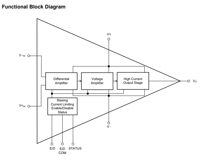
The OPA454 device is a low-cost operational amplifier with high voltage (100 V) and relatively high current drive (50 mA). The OPA454 device is a low-cost operational amplifier with high voltage (100 V) and relatively high current drive (50 mA). It is unity-gain stable and has a gain-bandwidth product of 2.5 MHz
The OPA454 is internally protected against overtemperature conditions and current overloads. It is fully specified to perform over a wide power-supply range of ±5 V to ±50 V or on a single supply of 10 V to 100 V. The status flag is an open-drain output that allows it to be easily referenced to standard low-voltage logic circuitry. This high-voltage operational amplifier provides excellent accuracy, wide output swing, and is free from phase inversion problems that are often found in similar amplifiers.
ENABLE and E/D Com
If left disconnected, E/D Com is pulled near V– (negative supply) by an internal 10-μA current source. When left floating, ENABLE is held approximately 2 V above E/D Com by an internal 1-μA source. Even though the active operation of the OPA454 results when the ENABLE and E/D Com pins are not connected, a moderately fast, negative-going signal capacitively coupled to the ENABLE pin can overpower the 1-μA pullup current and cause device shutdown. This behavior can appear as an oscillation and is encountered first near extreme cold temperatures. If the enable function is not used, a conservative approach is to connect ENABLE through a 30-Pf capacitor to a low-impedance source. Another alternative is the connection of an external current source from V+ (positive supply) sufficient to hold the enable level above the shutdown threshold.
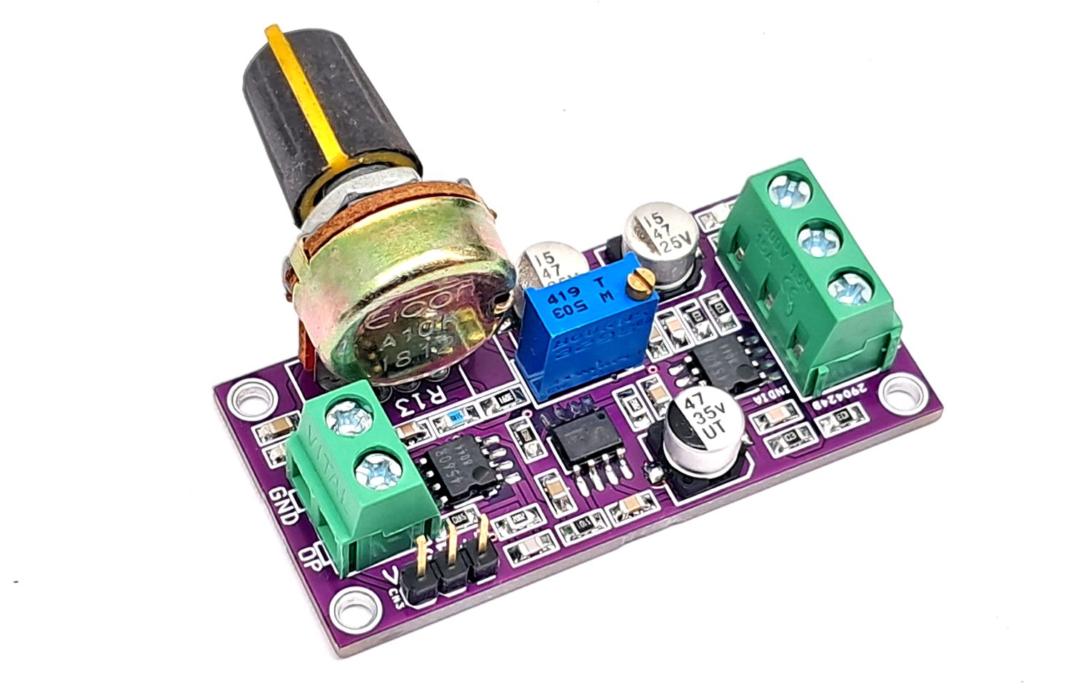
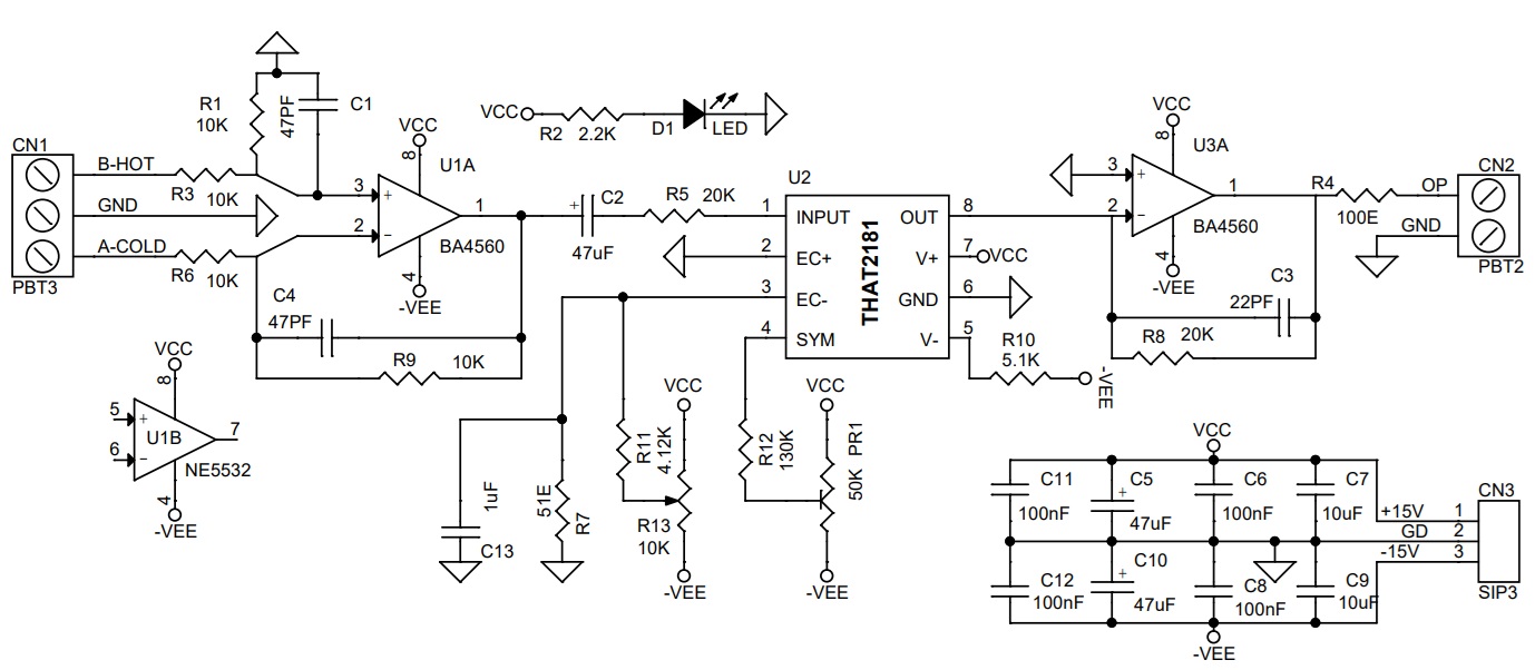
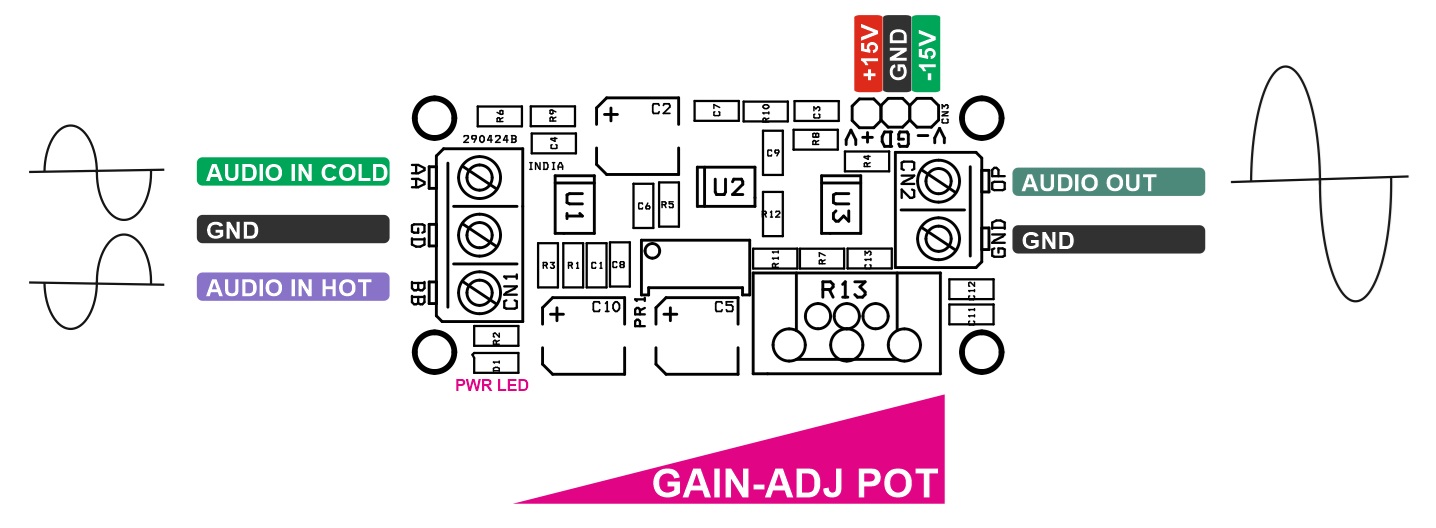
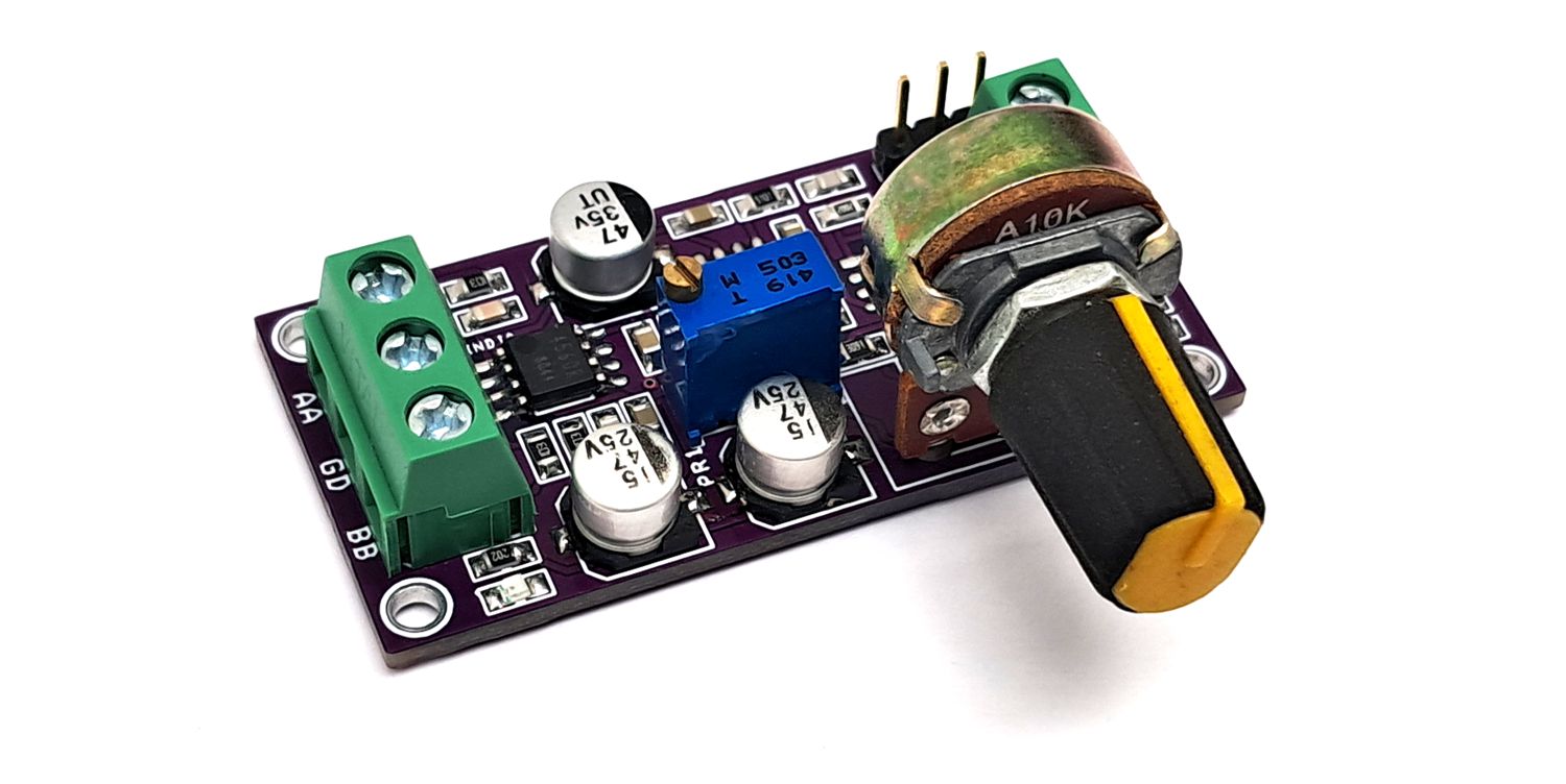
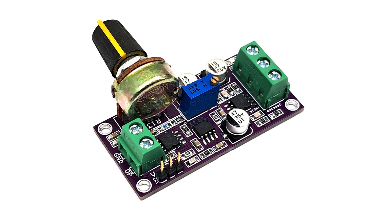
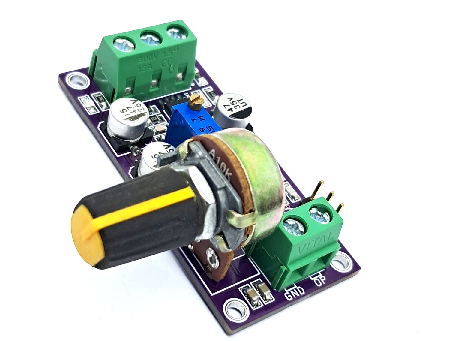
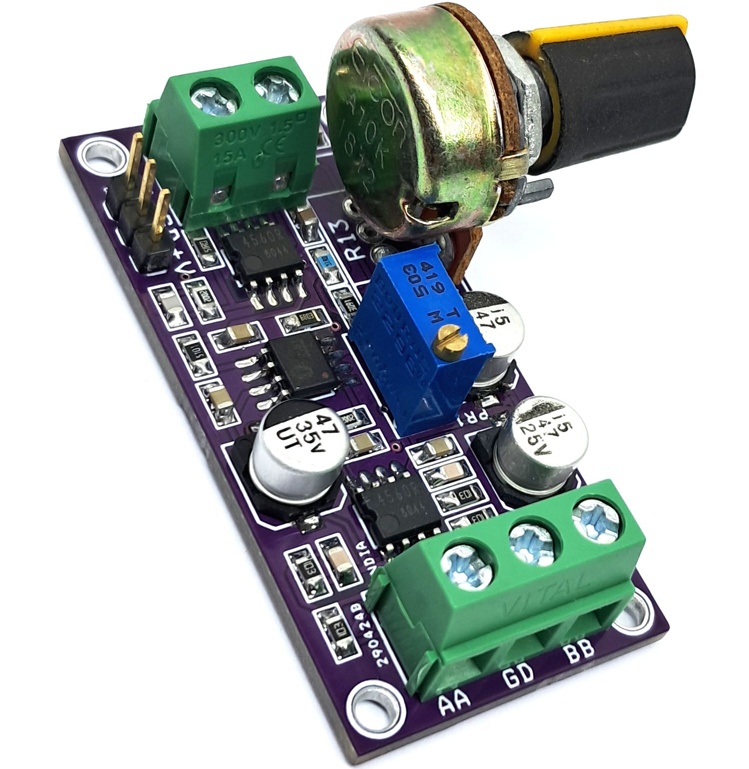
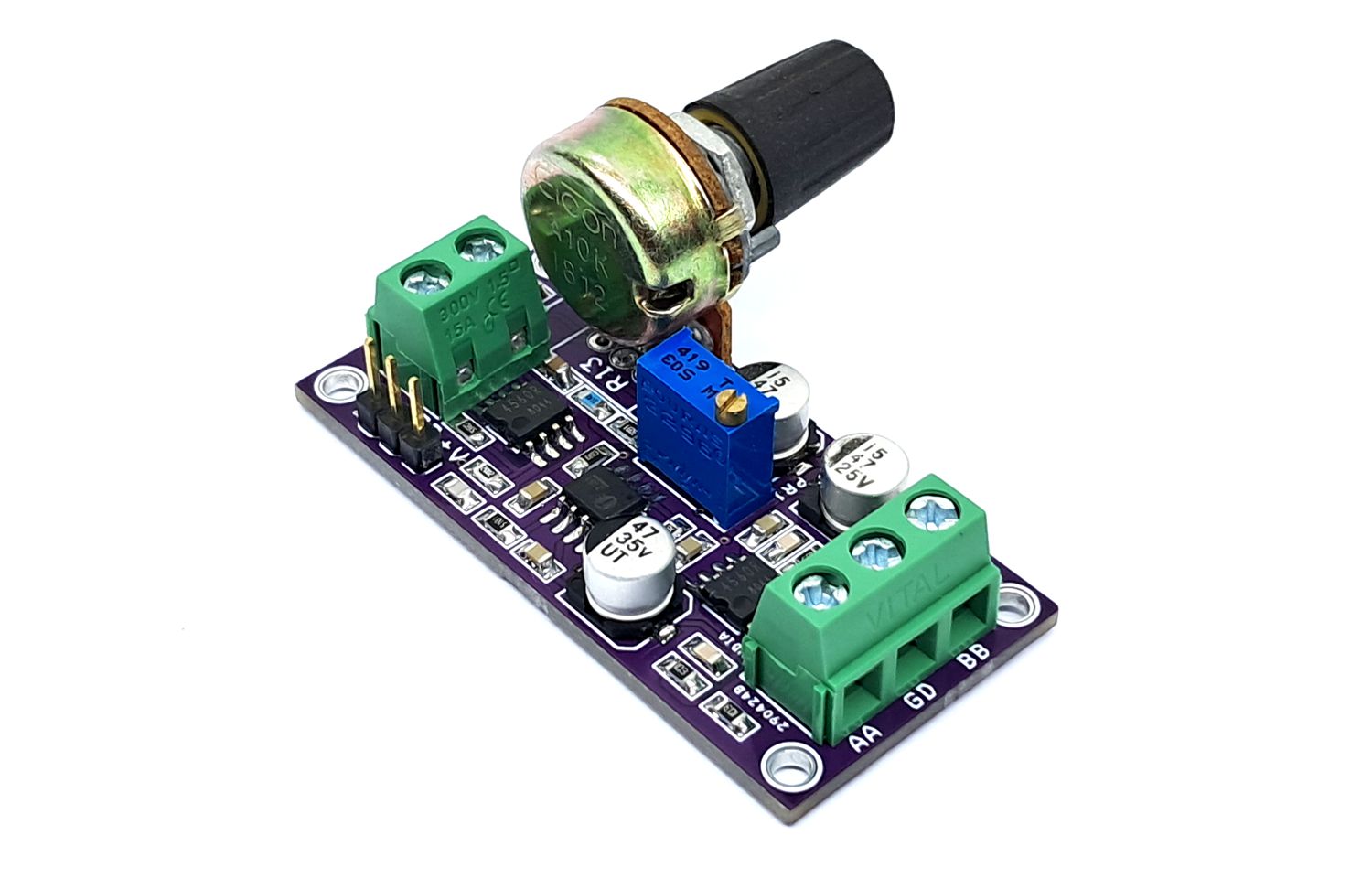
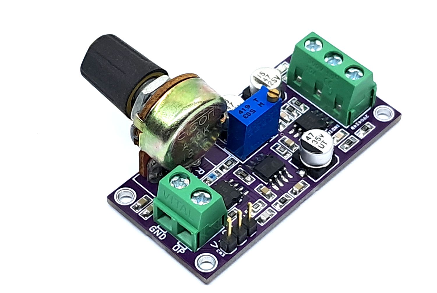
The project presented here is a Voltage Controlled Amplifier (VCA). A VCA board helps users control the audio level from a remote potentiometer. This board requires a balanced audio signal. Gain control voltage can be adjusted through potentiometer R13. The project works with a dual (±15V) power supply. Screw terminal connectors are provided for signal input and signal output. The project is built using THAT2181LA chip which is a VCA, designed for high performance in audio-frequency applications requiring exponential gain control, low distortion, wide dynamic range, and low control-voltage feedthrough. This chip controls the gain by converting an input current signal to a bipolar logged voltage, adding a DC control voltage, and re-converting the summed voltage back to a current through a bipolar antilog circuit. Stereo control of VCA with a single potentiometer is possible.
THAT2181–series trimmable Blackmer voltage-controlled amplifier (VCA) ICs are very high-performance current-in/current-out devices with two opposing-polarity, voltage-sensitive control ports. They offer wide-range exponential control of gain and attenuation with low signal distortion.
Trimming
The trim should be adjusted for minimum harmonic distortion using PR1. This is usually done by applying a middle-level, middle-frequency signal (e.g. 1 kHz at 1 V) to the audio input, setting the VCA to 0 dB gain, and adjusting the SYM trim while observing THD at the output. In 2181, this adjustment coincides closely with the setting which produces minimum control-voltage feedthrough, though the two settings are not always identical.
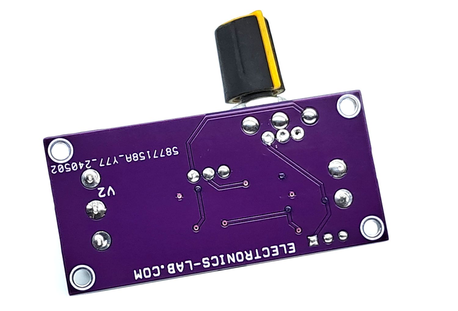
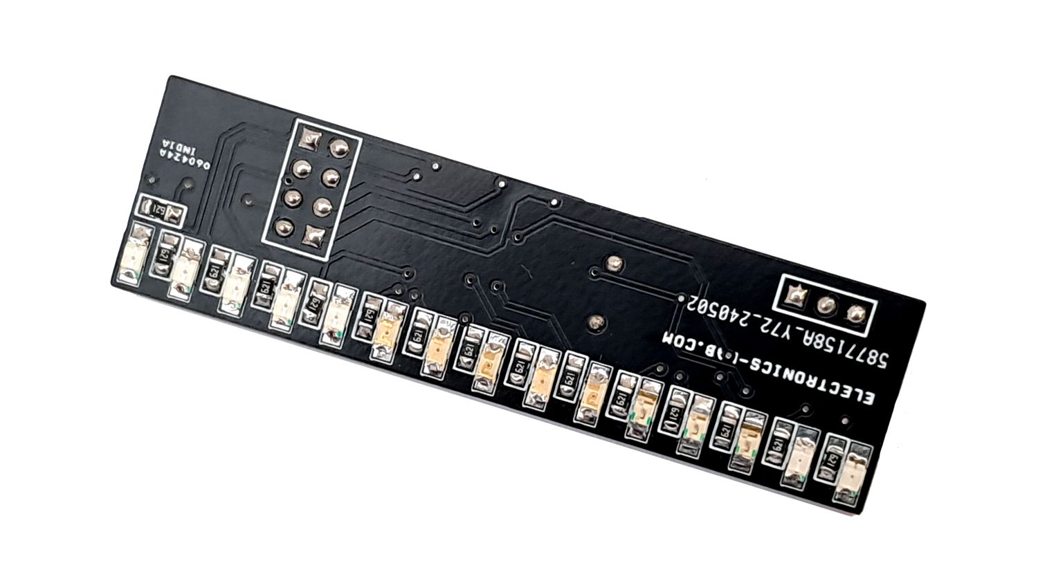
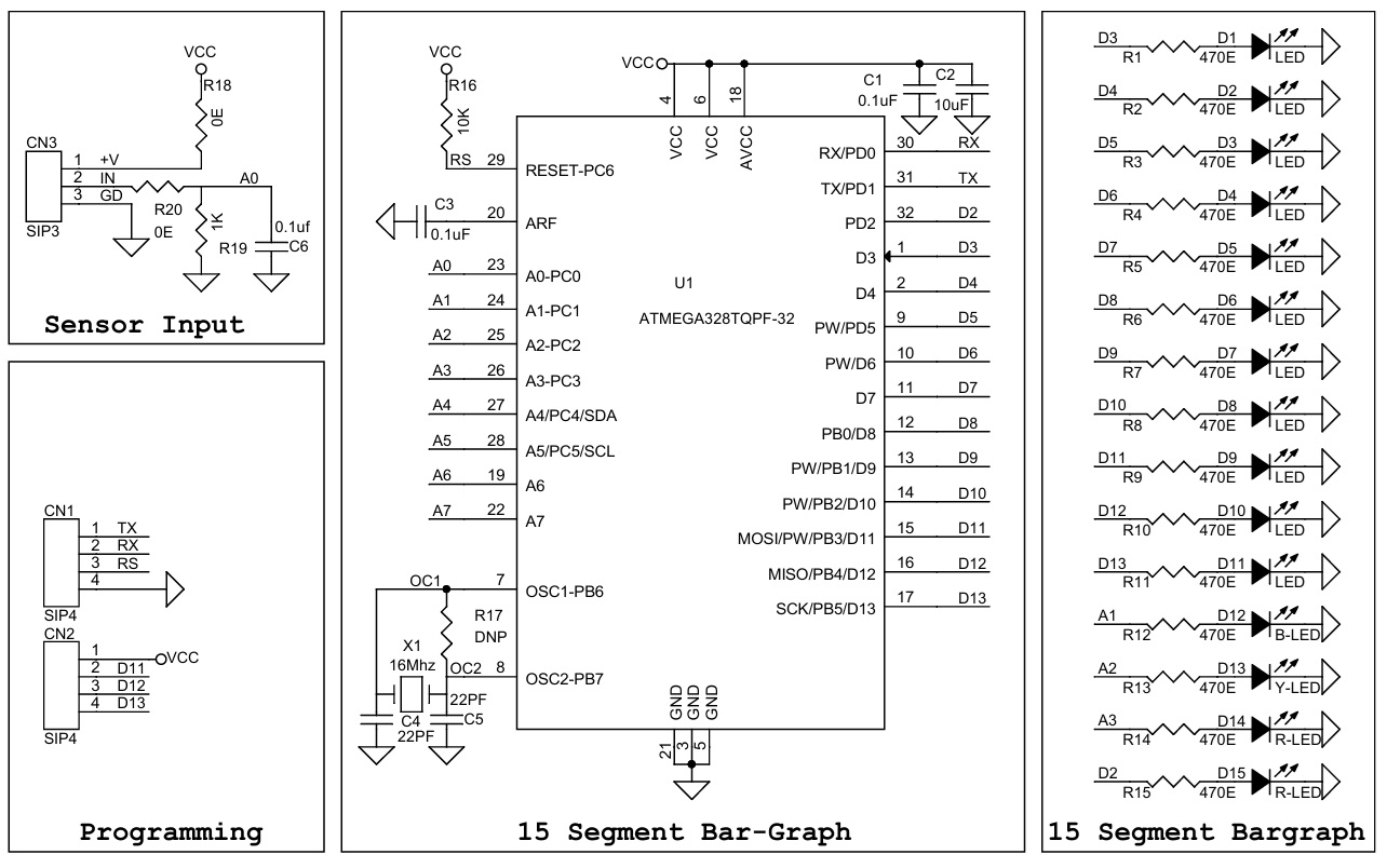
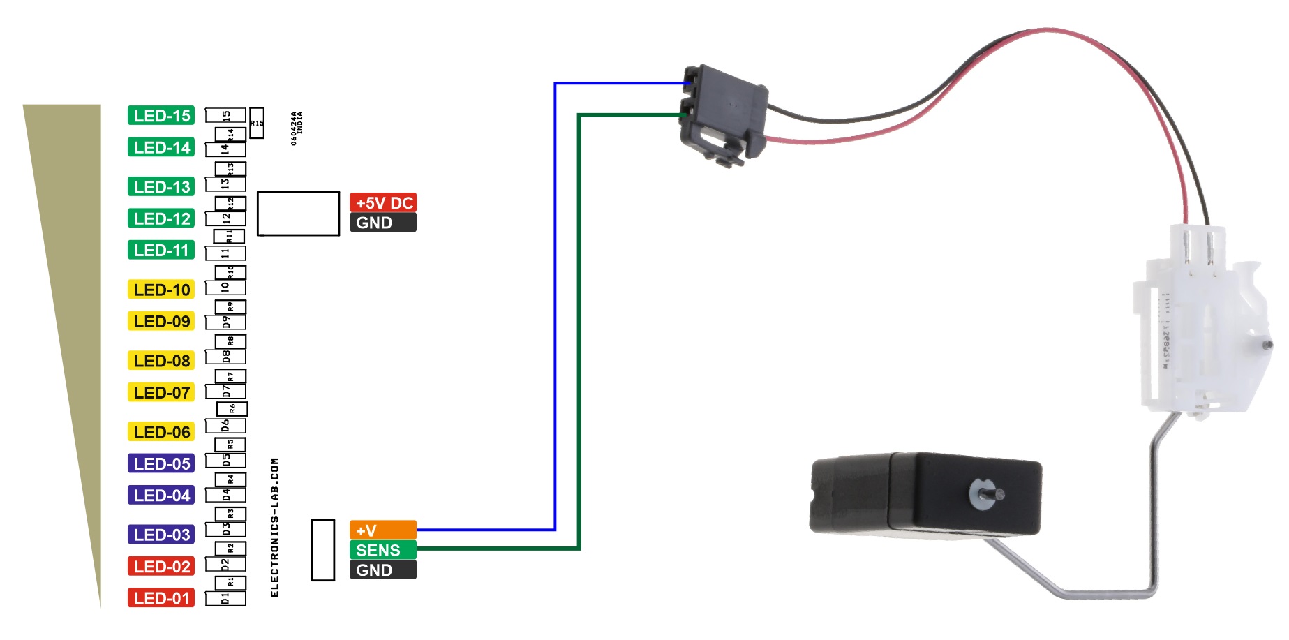
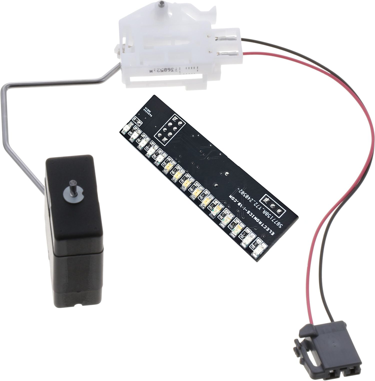
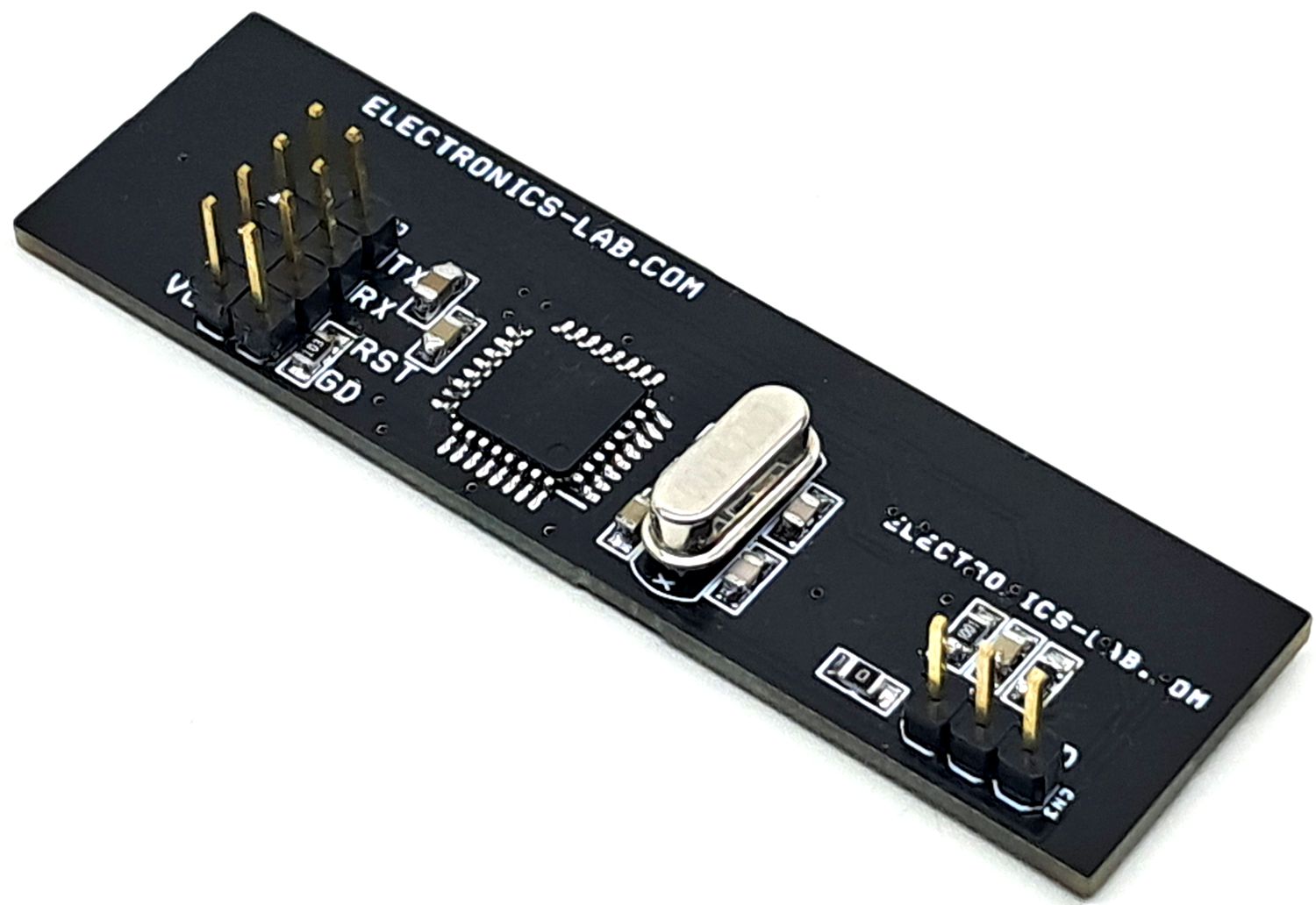
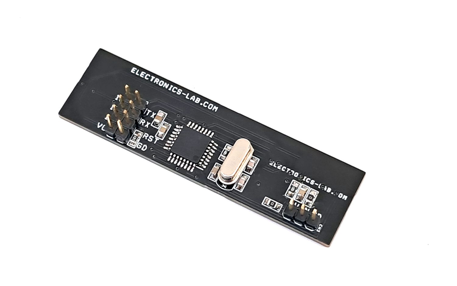
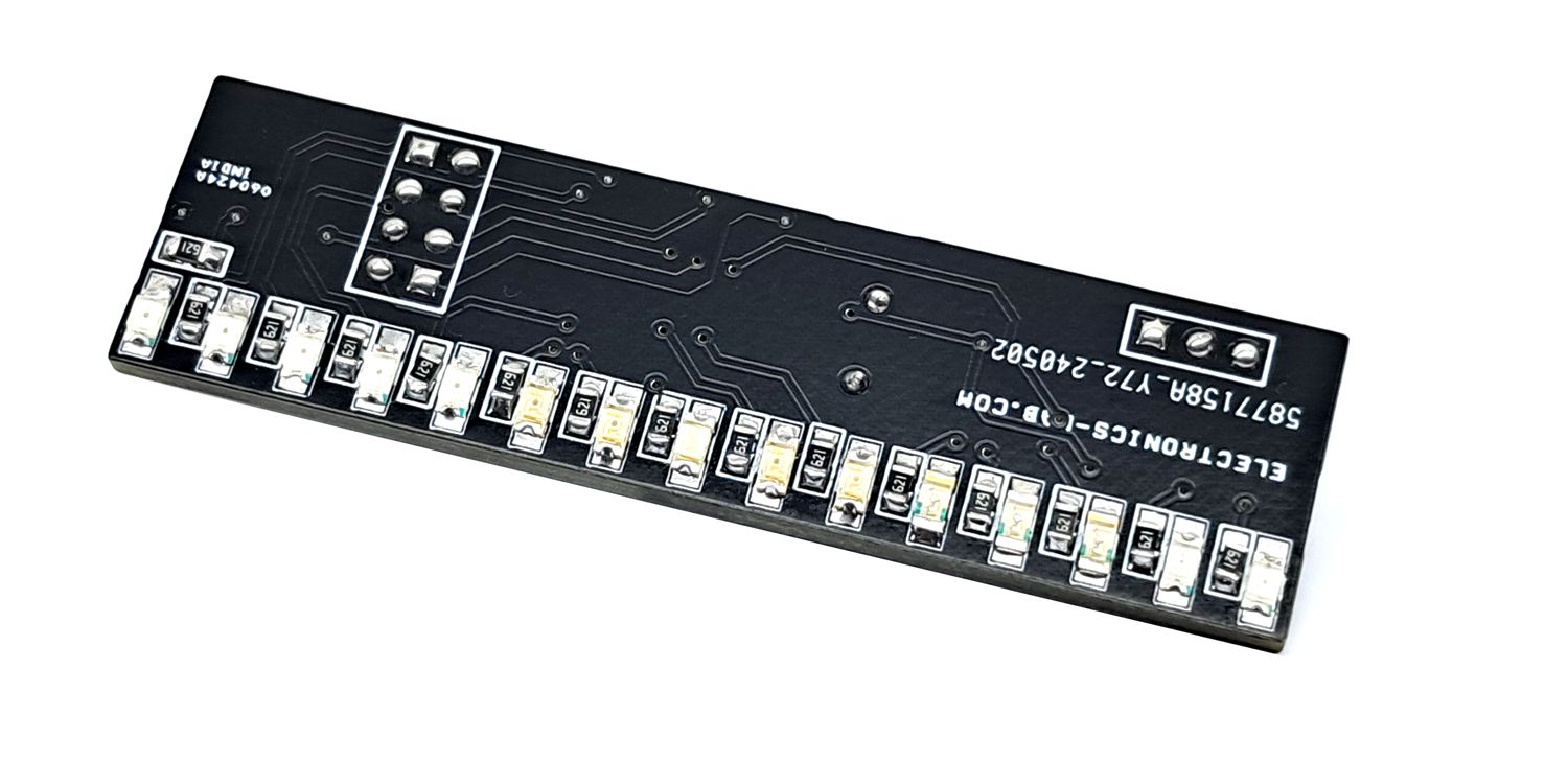
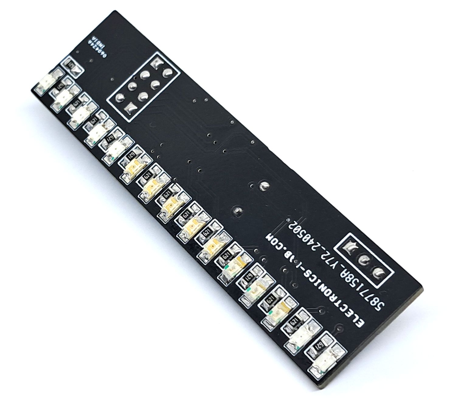
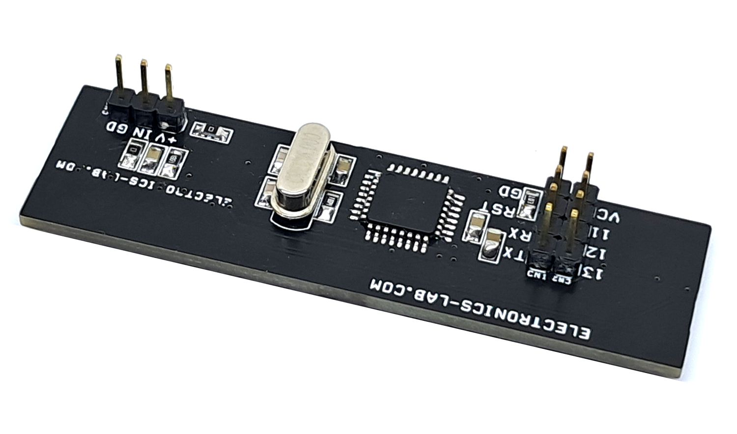
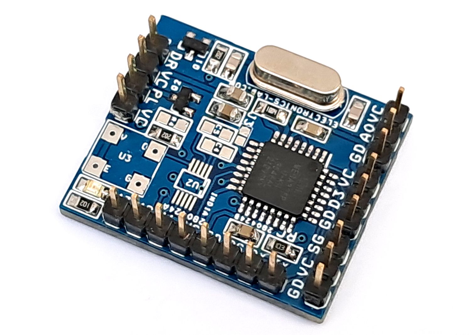
This Fuel level Monitor allows users to measure the fuel level using a resistive float sensor in the fuel tank. The project measures the fuel level and displays it on a 15-segment bar-graph display. The project is Arduino-compatible and consists of ATMEGA328 controller. The resistive sensor with a divider resistor is connected to Analog pin A0 of the MCU chip. The 15 LEDs of different colors are connected to various Arduino pins.
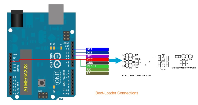
Arduino Code
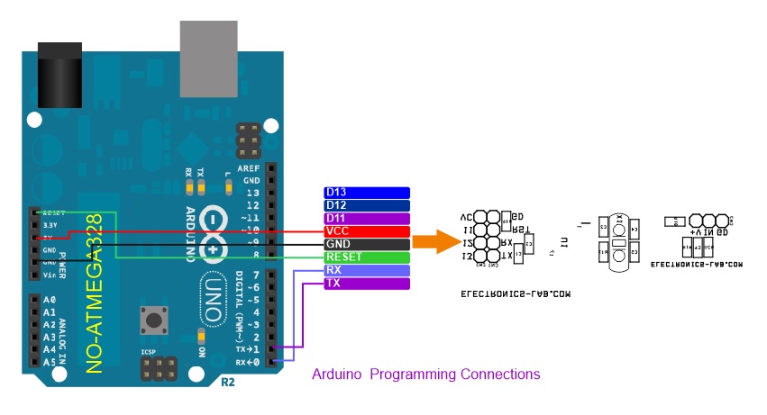
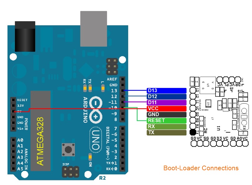
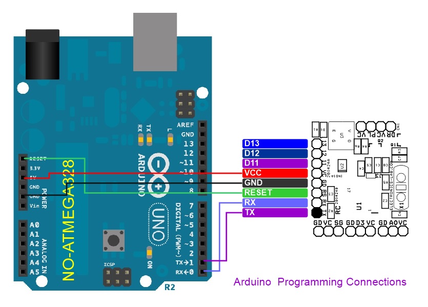
Arduino code is available to test the project. Burn the bootloader and code to a new ATMEGA328 microcontroller using the onboard programming connector. Refer to the connection diagrams below.
A resistive sensor is used to measure the fuel level. This sensor with 1kΩ divider resistor outputs analog values 785 to 984. This analog signal is connected to ADC A0 of the Arduino chip. Arduino chip evaluates input signal and controls 15LEDs. Different sensor provides different outputs. It is advisable to map the right value in Arduino code as per the sensor’s output.
Features
Power Supply 5V DC
15 Segments Bar-Graph Display
Arduino Compatible Project
Project Accommodates Any Resistive Sensor 2 Wire or 3 Wire
Multicolor LEDs Used for Easy Visualisation
On Board Connector for Bootloader and Arduino Programming
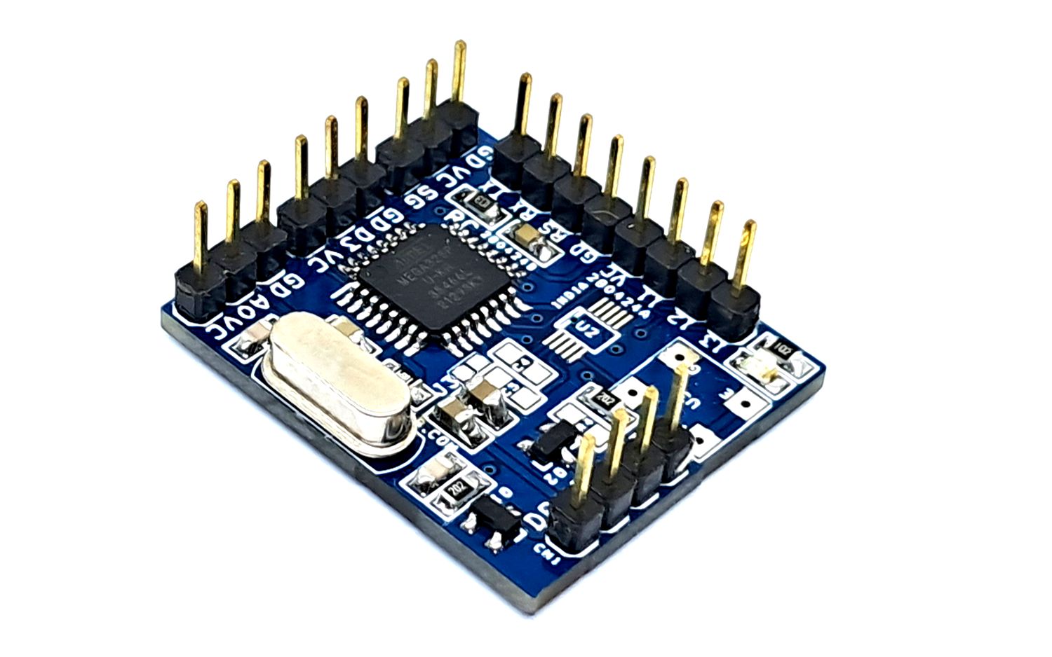
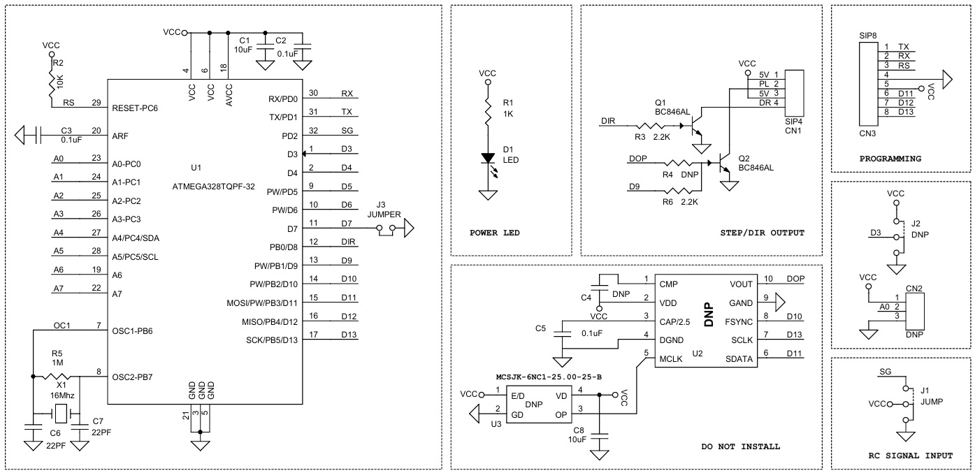
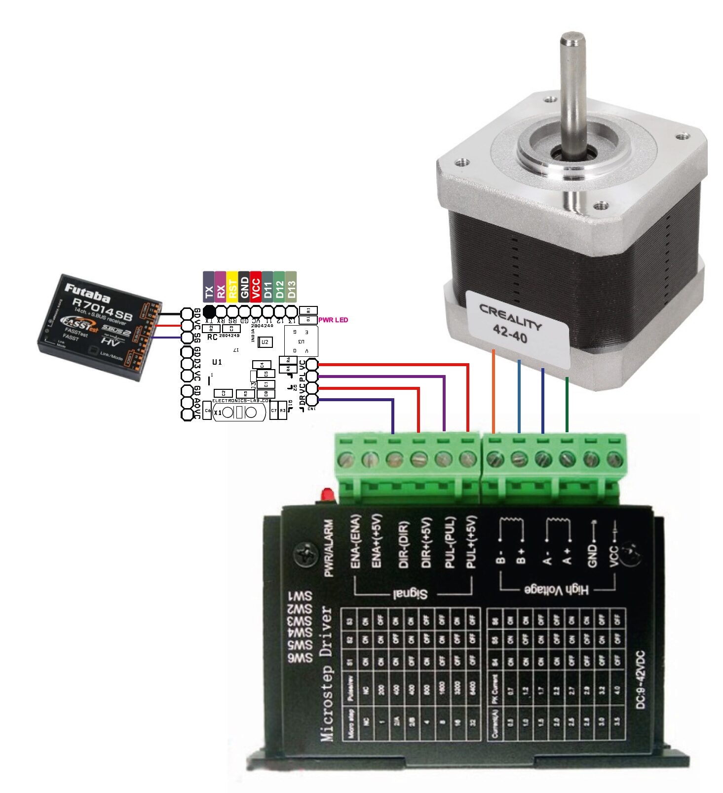
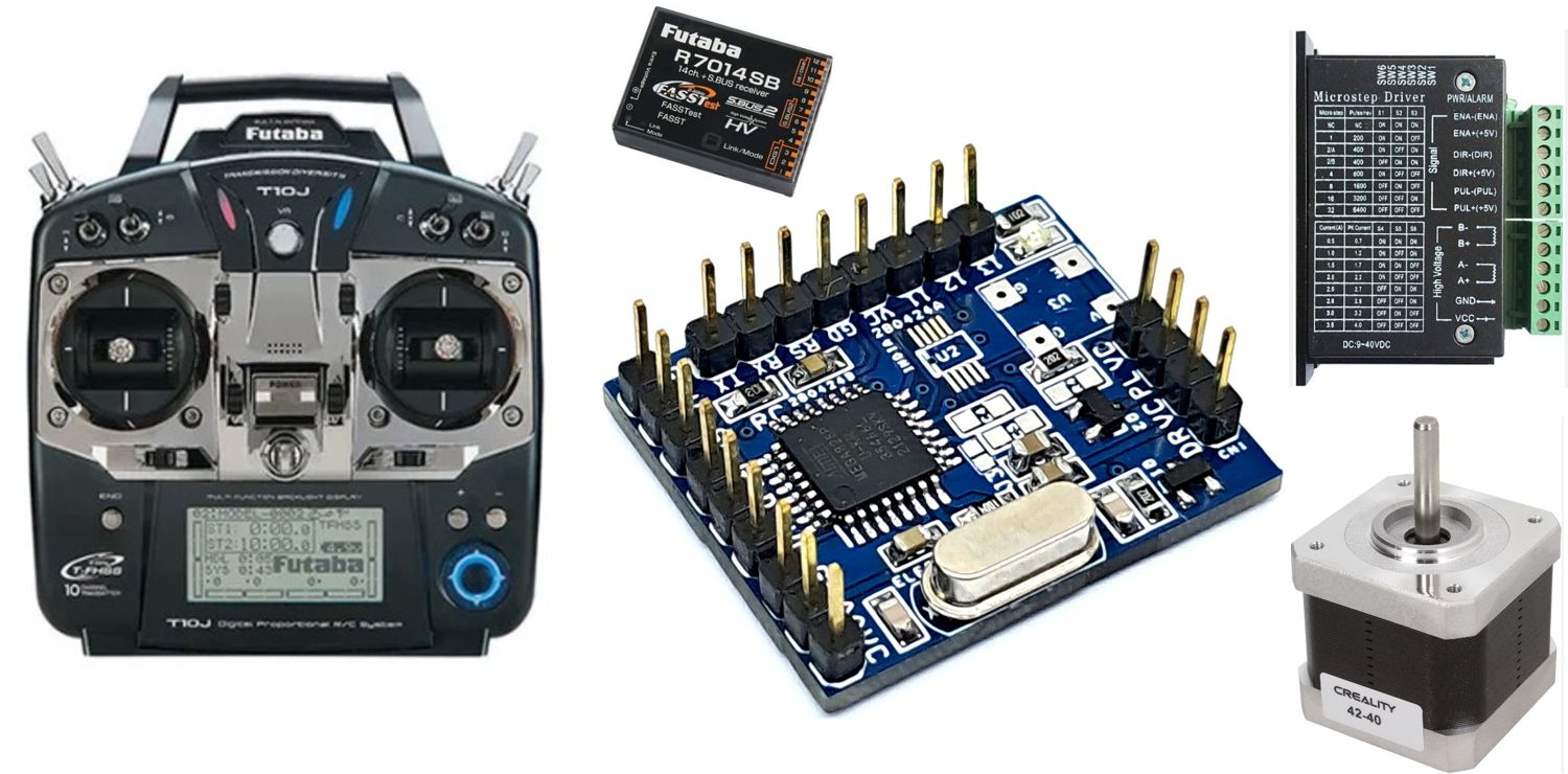
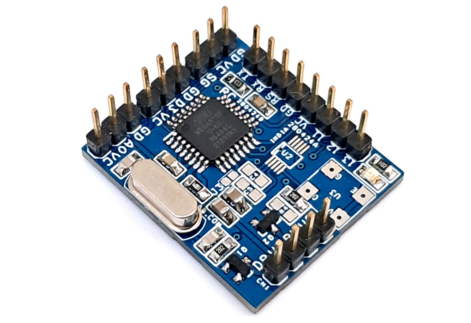
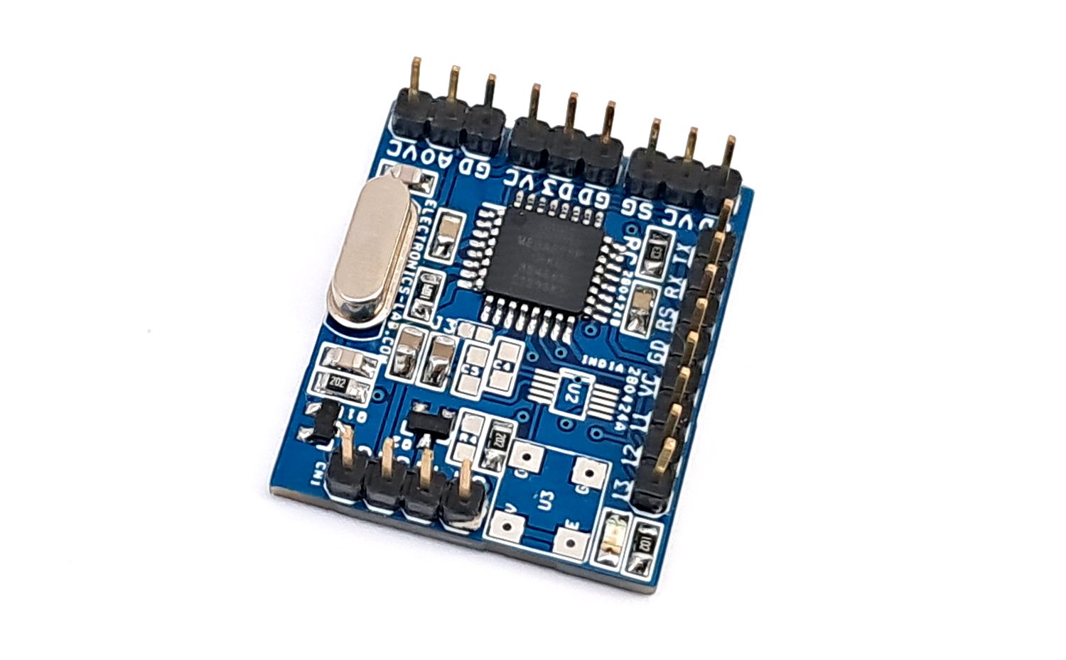
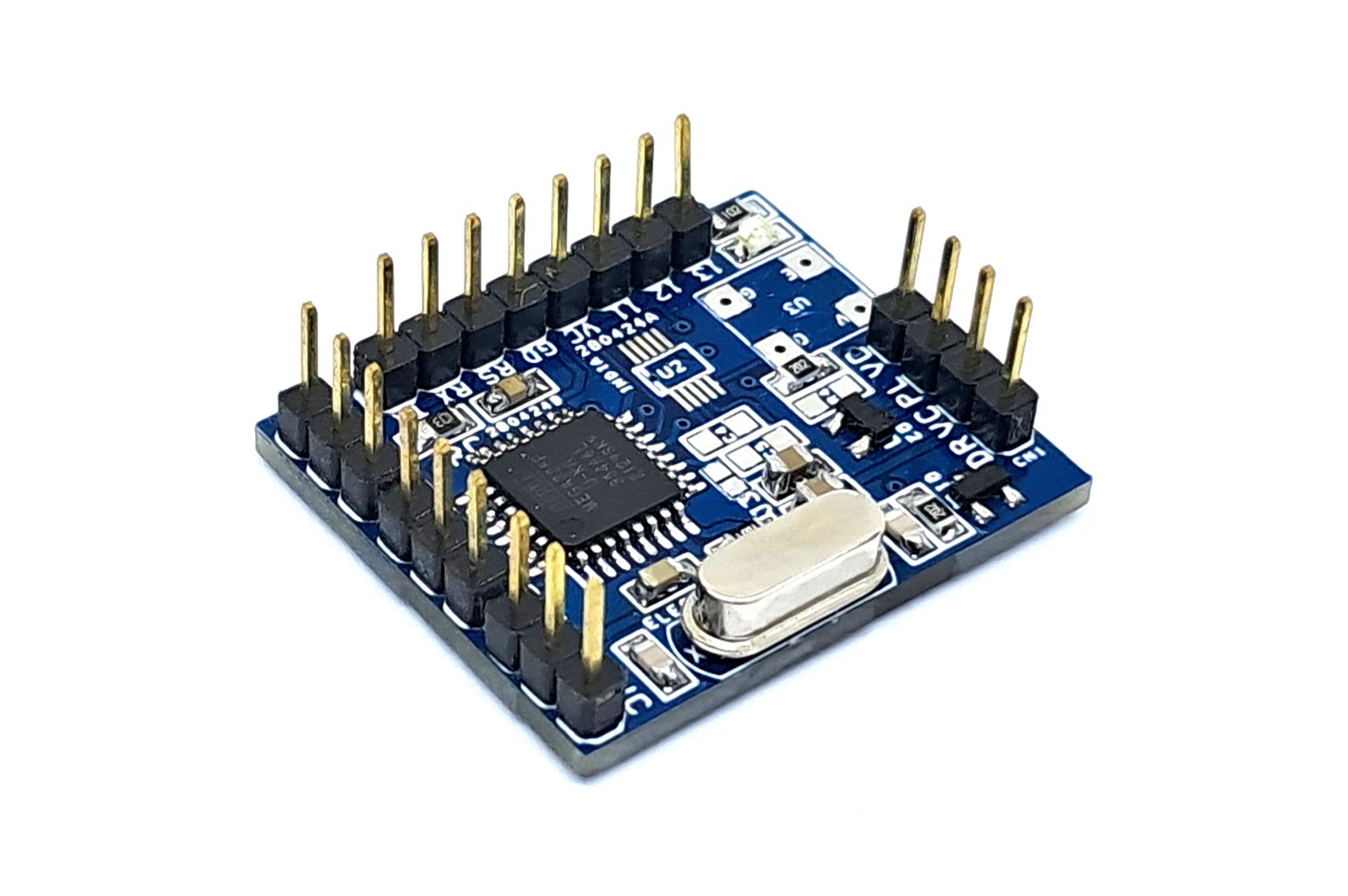
This simple Arduino compatible project reads an RC PWM signal (1000μs to 2000μs) and provides 0 to 500Hz pulse output to drive a stepper motor. Step and Direction outputs are open collector types 5V signals. Both signals can directly drive LEDs of optocoupler of stepper drivers. The board consists of ATMEGA328 chip and 2 x BC847 transistors. The transistor helps drive the optocouplers.
Arduino Code
A sample Arduino code is available to test the project.
Burn the bootloader and Arduino code into the new ATMEGA328 microcontroller using an onboard programming connector. Refer to the bootloader and Arduino programming diagram for Connections.
Credits: This is modified code, original code written by: Brandon Tsuge (theboredrobot.com)
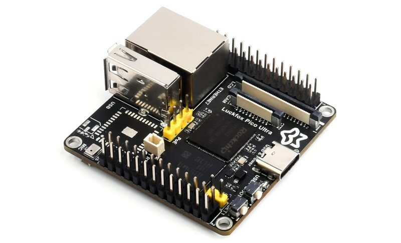
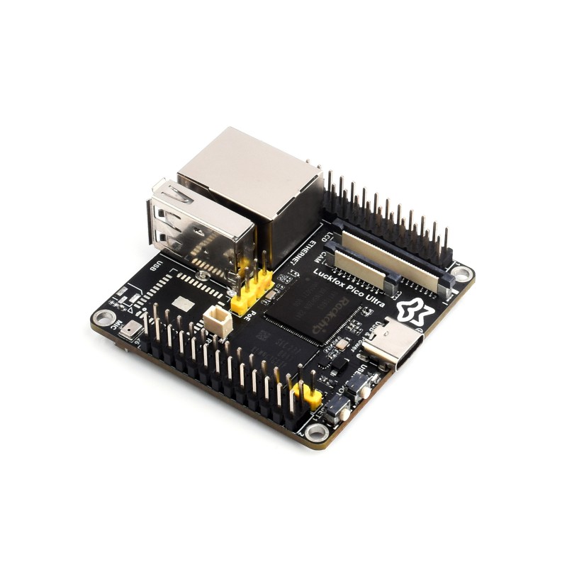
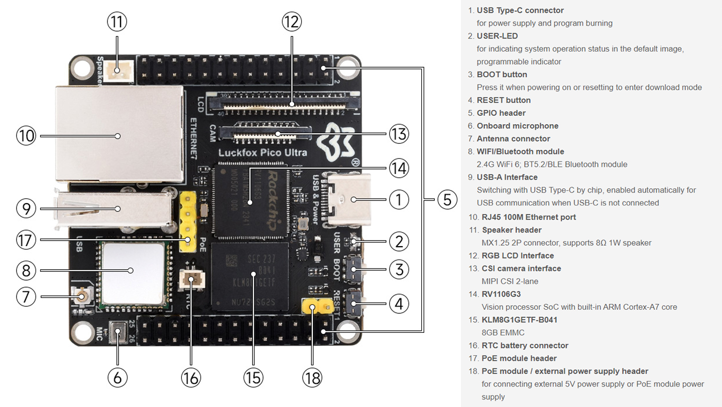
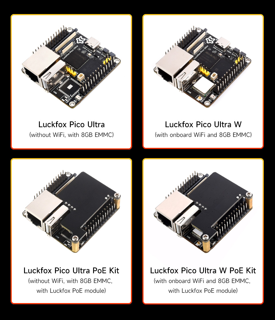
Luckfox Pico Ultra is a Rockchip RV1106-based micro Linux dev board with 0.5 Tops NPU to run AI that can be configured to run AI tasks. The board also features a MIPI CSI port, an Ethernet port GPIO, UART, RGB LED header, SPI, I2C, USB, a speaker interface, and much more. Waveshare also offers two variants of this board one with the wireless module (The W variant) and one without the wireless module, both modules can be equipped with PoE HATs so there are four variants available for this dev board Kit.
In terms of features and specification, the board is very similar to the LuckFox Pico Pro and Pico Max that we wrote about a few months back but the only difference is the form factor and the option to add a wireless module and/or PoE support. Additionally, we have written about dev boards like the feel free to check those out if you are interested in the topic.
The Rockchip RV1106G3 is a fourth generation of Rockchip NPU that supports int4, int8, and int16 hybrid quantization meaning that this NPU can deliver 0.5 TOPS when using int8, and 1.0 TOPS with int4. Additionally, it has support for third-generation ISP 3.2 with support for up to 5 megapixels camera module, High Dynamic Range and Wide Dynamic Range algorithms.
Luckfox Pico Ultra Specifications
SoC: Rockchip RV1106G3
CPU: Arm Cortex A7 @ 1.2GHz with an integrated RISC-V co-processor
NPU: 0.5 TOPS, supports INT4/INT8/INT16, compatible with TensorFlow, MXNet, PyTorch, Caffe, Onnx NN
10/100Mbps Ethernet controller and embedded PHY with optional PoE
2.4GHz WiFi 6 and Bluetooth 5.2/BLE (available only in Luckfox Pico Ultra W)
USB Ports:
1x USB-C port
1x USB-A port (switches with USB Type-C by chip, enabled automatically for USB communication when USB-C is not connected)
GPIO:
2x 26-pin headers
Miscellaneous:
BOOT and RESET buttons
User LED
RTC battery connector
PoE module header
Power Supply:
5V via USB-C port or PoE port (802.3af compatible)
Dimensions:
50 x 50 mm
In terms of software, the board supports build root and Ubuntu 22.04 systems, and as mentioned earlier the board comes in four variants so you can customize the one that fits your needs at the time of purchase. You can find more details about the products on the Waveshare wiki page.
The Luckfox Pico Ultra dev board is available on AliExpress for $26.27+ based on options like WiFi and PoE. It will soon be on Amazon. It can also be bought from Waveshare’s official store for $17.99-$29.99, excluding shipping.
ilyT-Glass is an ESP32-S3-powered smart glasses with a smart Bosch AI IMU. The Bosch IMU is an AI smart sensor that integrates a 6-axis IMU, a 32-bit customizable programmable microcontroller, and various software functionalities. With these functionalities, this can be used in applications like navigation, machine learning analytics, and orientation estimation. All the main features of this board are very similar to the Google Glass2 but with open-source code and a lot of room for development.
The display used in this glass is a JD9613 full-color LTPS AMOLED display with 294 x 126 pixels of resolution, but the actual display area is less than the full display spec of the module as there is a prism attached in the form of the glass to give it a 3D look.
Previously we have written about Voxos smart glasses and other smart glasses feel free to check that out if you are interested in the topic.
Looking at the BHI260AP sensor we find that it is an always-on type self-learning sensor with a 6-axis IMU, and a 32-bit MCU with example software and ML models making it ideal for remote monitoring applications. It also supports sophisticated machine learning analytics, which makes it easy to capture precise motion.
LILYGO T-Glass Specifications
Wireless SoC: Espressif Systems ESP32-S3FN4R2
CPU: Dual-core Tensilica LX7, capable of up to 240 MHz, with vector instructions for AI tasks
Memory: 512KB RAM, 2MB PSRAM
Storage: 4MB flash
Wireless: 2.4 GHz WiFi 4 and Bluetooth
Display:
1.1-inch LTPS AMOLED, JD9613
Resolution: 294 x 126 pixels
Full color
Sensor:
BOSH BHI260AP includes a 6-axis IMU and AI features
Audio:
Integrated microphone
Interface:
Touch-sensitive button
USB:
1x USB Type-C port for power (5V/500mA) and programming
Additional Features:
Real-Time Clock (RTC)
3D-printed holder for the prism display
Example open-source software provided
Dimensions:
Glass: 140 mm
Display mount: 160 mm x 80 mm
Weight: Not specified
3D Printed Component:
Prism display mount
More information about the product along with code like real-time clock, touch buttons, and voice activity detection can be found on the company’s GitHub repository.
The LILYGO T-Glass can be purchased from both Amazonand Aliexpress, on Amazon it’s priced at $48, and on Aliexpress it’s also priced the same, it can also be purchased directly from the LILYGO store, but currently at the time of writing it’s out of stock in every location.
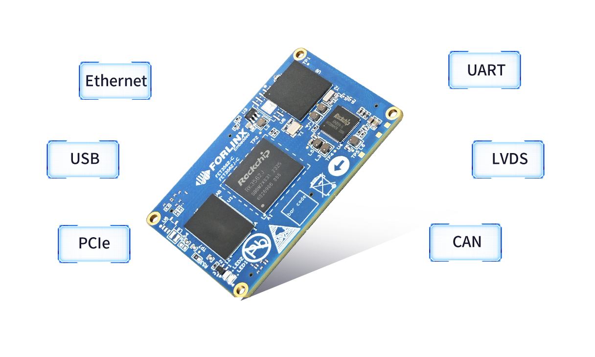
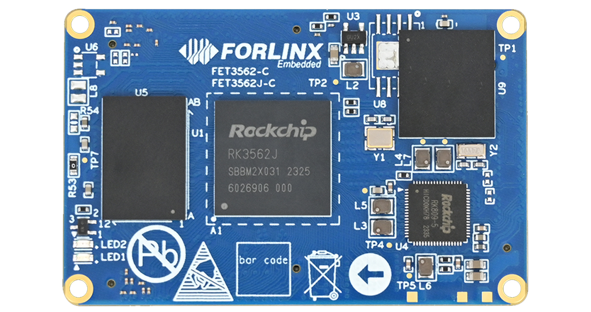
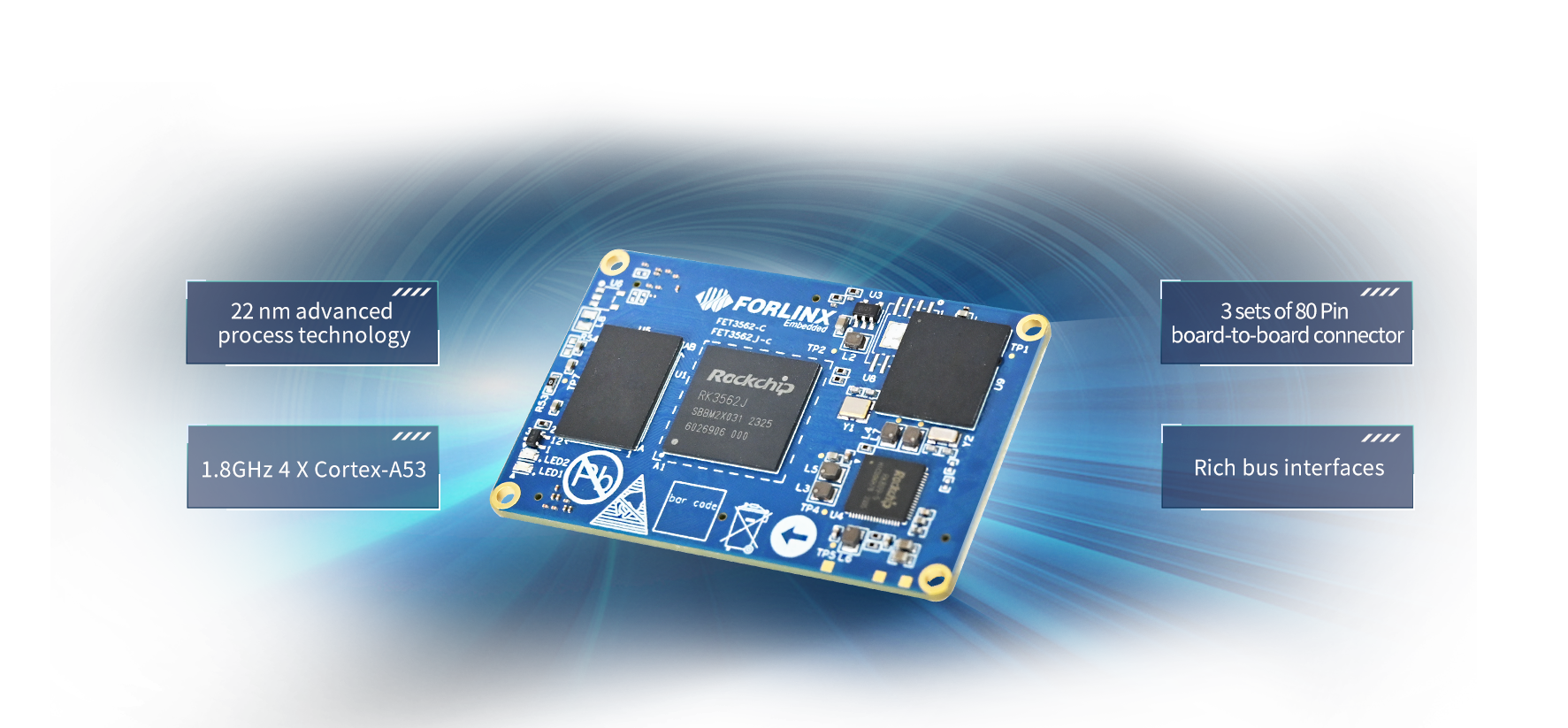
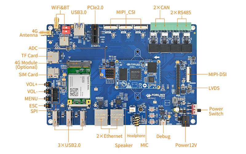
Forlinx FET3562J-C is a Rockchip RK3562/RK3562J-based System On Module (SoM) designed for IoT, automation, and consumer electronic applications. The SoC used in the module is built with the latest 22nm process with ARM Cortex-A53 cores running at up to 2GHz, which makes it very power-efficient. In terms of storage, it can be configured with LPDDR4 RAM and can be configured with up to 16GB eMMC storage.
Additionally, it features 1 TOPS NPU, Ethernet, Wifi, Bluetooth, LVDS, MIPI DSI, and much more. Making this device useful for applications like IoT, automation, and consumer electronic applications.
The company offers a System on Module (SoM) that can be configured with either the RK3562J or the RK3562 SoC. The RK3562 features 2.0GHz ARM Cortex-A53 cores and a 1 TOPS NPU, delivering higher processing speeds. In contrast, the RK3562J has cores clocked at up to 1.8GHz, ensuring reliable operation in a temperature range of -40 to +85°C, but it does not include an NPU. This SoM supports various graphics and compute acceleration technologies, including OpenGL ES 1.1/2.0/3.2, OpenCL 2.0, and Vulkan 1.1. It is also equipped with a dedicated 2D hardware engine and a high-quality JPEG encoder and decoder.
The company also offers a carrier board, to you can attach the som and access all its functionality that is shown above.
Forlinx FET3562J-C SoM and Carrier Board specifications
SOM Specifications
Processor Options:
Rockchip RK3562J:
CPU: 4× Cortex-A53 @ 1.8GHz
NPU: None
Rockchip RK3562:
CPU: 4× Cortex-A53 @ 2.0GHz
NPU: 1TOPS INT8, supports INT4/INT8/INT16/FP16
Graphics and Video:
GPU: Mali-G52-2EE
Supports OpenGL ES 1.1/2.0/3.2, OpenCL 2.0, Vulkan 1.0/1.1
The company has not released any pricing information for the Forlinx FET3562J-C SoM. More information about the Rockchip RK3562(J) system-on-module and associated development board can be found on the product page.
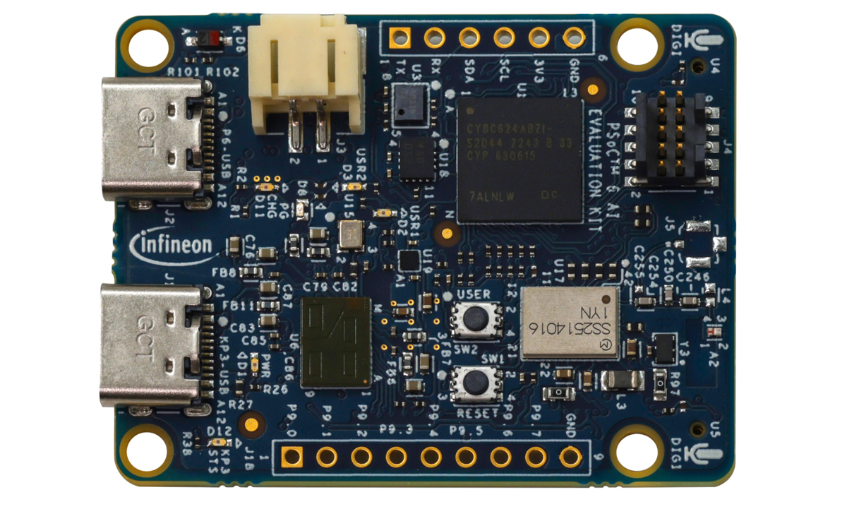
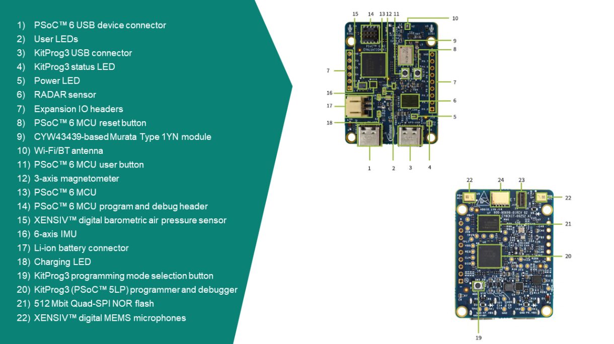
Infineon CY8CKIT-062S2-AI Dev Kit is a PSoC 62S2 MCU-powered development board built to create and test edge AI applications. The unique aspect of this board is that it features a plethora of sensors including a microphone, radar, IMU, magnetometer, and an air pressure sensor which can be configured to get environmental data, and with the help of a prebuilt AI model that data can be processed very easily.
In terms of connectivity the board has Wi-Fi and Bluetooth connectivity and complementing that is an additional expansion header that can be used to connect extra sensors and modules. This feature with an AI-compatible processor makes this device useful for applications like industrial monitoring, wearables, healthcare devices, robotics, and more.
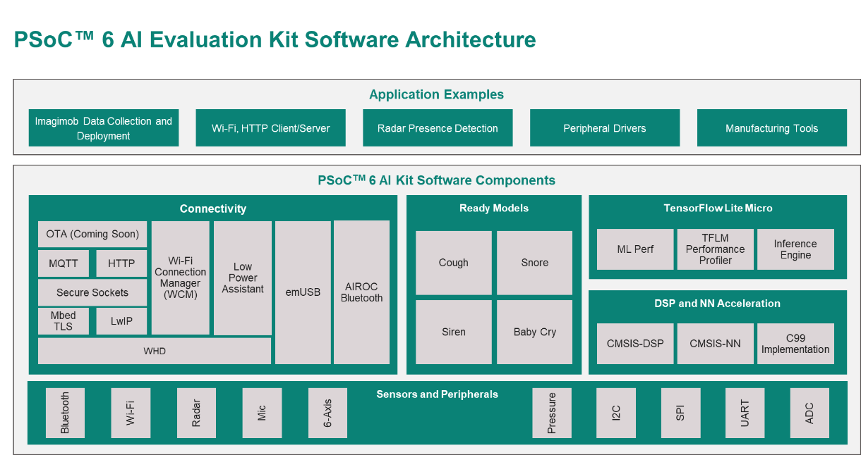
The most unique aspect of this board is its software support as it comes with ready-to-use machine learning models which makes it easy to develop Edge AI applications around it, also it has support for ModusToolbox, Infineon’s software tool for embedded development and we have seen it used in the PSoC 64 IoT Security Workshop Development Kit. The board also supports the Imagimob Studio platform with which you can create machine-learning models and use them on small devices.
Infineon CY8CKIT-062S2-AI Dev Kit Specifications
MCU: PSoC 62S2 (Arm Cortex-M4F and Cortex-M0+, up to 1MB Flash, 288KB SRAM)
Wireless: Murata LBEE5KL1YN-814 (Wi-Fi 4, Bluetooth 5.2)
The Infineon CY8CKIT-062S2-AI Dev Kit also supports TensorFlow Lite Micro and neural network acceleration via CMSIS-DSP and CMSIS-NN libraries. This, combined with MQTT, HTTP, and AIROC Bluetooth connectivity, facilitates rapid prototyping and AI application development. The kit is available for purchase at $37.50 on Mouser Electronics and $50 on DigiKey.