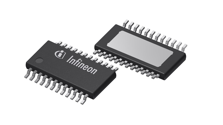
LITIX™ Power TLD5191ES is a synchronous 4 – switch buck-boost DC/DC controller with built-in protection features.
This concept is beneficial for driving high-power LEDs with maximum system efficiency and a minimum number of external components for automotive exterior lighting.
Key features
MOSFET 4 – switch buck-boost DC/DC controller for high power buck-boost LED control
Constant current and constant voltage regulation
Wide VIN range (4.5 V to 40 V)
Wide LED forward voltage range (Vout range from 2 V to 55 V)
Additional features
LED current accuracy +/-3% at Tj=25° C and 4% over the whole automotive temperature range
Switching frequency range from 200 kHz to 700 kHz
Maximum efficiency in every condition (up to 96%)
EMC optimized device: spread spectrum always active
Overvoltage, shorted LED fault, and over-temperature diagnostic outputs
Adjustable soft start
Enhanced dimming features: analog and PWM dimming (from digital input or sourced by embedded PWM engine)
Available in a small thermally enhanced TSDSO-24 package
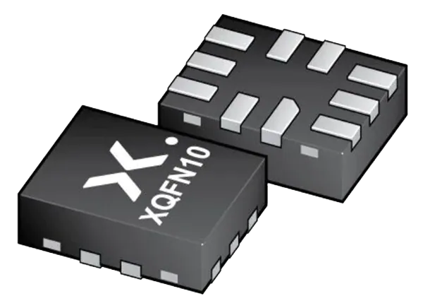
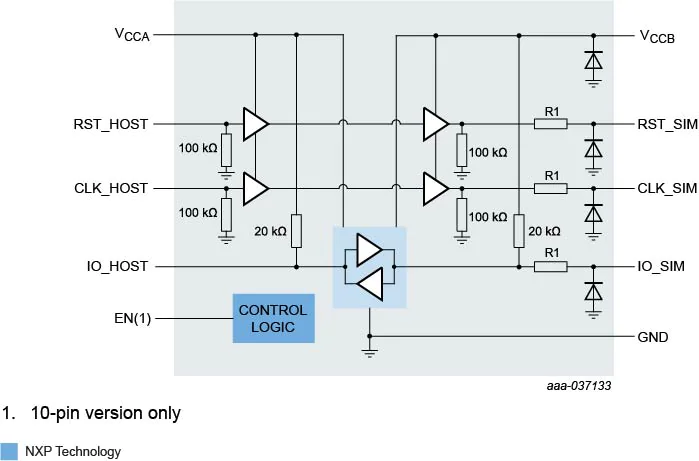
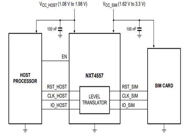
Nexperia NXT4557 SIM Card Interface Level Translator is built for interfacing a SIM card with a single low-voltage host-side interface. The NXT4557 consists of three-level translators to convert the data, RST, and CLK signals between a SIM card and a host microcontroller. The translator features a high-speed level translation capable of supporting class-B, class-C SIM cards, and HIGH EN pin that enables the normal operation of the translator. The device is compliant with all ETSI, IMT-2000, and ISO-7816 SIM/Smart card interface requirements. Typical applications include a wide range of SIM card-attached devices, including mobile and personal phones, wireless modems, and SIM card terminals.
Features
Support SIM cards and eSIM with supply voltages 1.62V to 3.3V
1.08V to 1.98V host micro-controller operating voltage range
Automatic level translation of I/O, RST, and CLK between SIM card and host side interface with capacitance isolation
Incorporates shutdown feature for the SIM card signals according to ISO-7816-3
High Vdis(UVLO_AC) switching level, arranging quick shut down when VCC_SIM powers down
Integrated pull-up resistors; no external resistor required
Integrated EMI Filters suppress higher harmonics of digital I/Os
A HIGH EN signal enables the translation of the signals
Low current shutdown mode <1μA
Supports clock speed beyond 5MHz clock
Pb-free, Restriction of Hazardous Substances (RoHS) compliant, and free of halogen and antimony (Dark Green compliant)
ESD protection:
HBM ANSI/ESDA/JEDEC JS-001 exceeds 2kV
CDM ANSI/ESDA/JEDEC JS-002 exceeds 1kV
IEC61000-4-2 level 4, contact and air discharge on all SIM card-side pins are 8kV and 15kV
Rigol has created a 7GHz differential probe to go with the 5GHz DS70000 oscilloscopes that it announced at the beginning of the year.
Called PVA8000, the probe also comes in a 3.5GHz variant, and there are single-ended types. Inside is the same ‘Phoenix’ ASIC that the company designed for the scopes.
“As soon as you connect a probe to the DS70000, it is automatically recognized by the oscilloscope and a calibration is requested, which can be carried out on the oscilloscope,”
according to the company.
Typical minimum rise time is 70ps, and the (frequency-dependent) common-mode rejection can be as high as 40dB. The inputs present 50kΩ to differential sources (25kΩ single-ended).
“With the differential version, the distance between the tips can be adjusted quickly,” according to the company. “You can also store three different distances and call them up again automatically at the push of a button.”
LEDs on the probes show the same color as the scope’s input channel.
To help reach a variety of physical situations, four different probe heads are included.
The single-ended probe has three different probe tips for a thermistor and four different terminals for the ground connection. Three replacement pins are supplied as standard.
“In addition, an additional probe is available for both variants, where the wires can be soldered to the device-under-test,” said Rigol. “Here, too, a replacement wire and a ruler for measuring the exact length of the replacement wire are included as standard.”
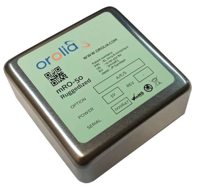
Orolia has introduced a ruggedised version of its mRO-50 miniature (51 x 51 x 20mm) rubidium atomic clock.
Called ‘mRO-50 Ruggedized’, its vibration rating has been raised from 4Grms to 7.7Grms (lock retained, MIL-STD-810H method 514.8 annex E – was annex C), and shock raised from 30G to 50G (MIL-STD-202G 11ms half sine) – qualification to the shock rating is still on-going, according to the datasheet.
Maximum temperature of the thermal chamber (with air flow around unit) is now -40 to +80°C, which was an option on the standard model – which is normally rated only -10 to 60 or +65°C.
Timing specifications include one-day hold-over <1µs, said Orolia. Lock is <2 minutes at over the full temperature range.
The unit weighs 80g and consumes 45mW (1.5W at start) in the 5V version and 360mW (1W) in the 3.3W version.
Underwater, military communications, radar, low earth orbit, electronic warfare, airborne and unmanned vehicle applications are forseen.
Based in Neuchatel Switzerland, Orolia was founded in 2006 and has supplied timing products to ESA, NASA, JPL, Space-X, Blue Origin, NPL, CNES, DLR and JAXA. ESA awarded itcontracts to provide atomic clocks for the first 12 satellites for the Galileo 2nd generation. – each satellite will contain three of its Rubidium atomic frequency standards and two of its atomic clock physics packages integrated with Leonardo’s passive hydrogen masers.
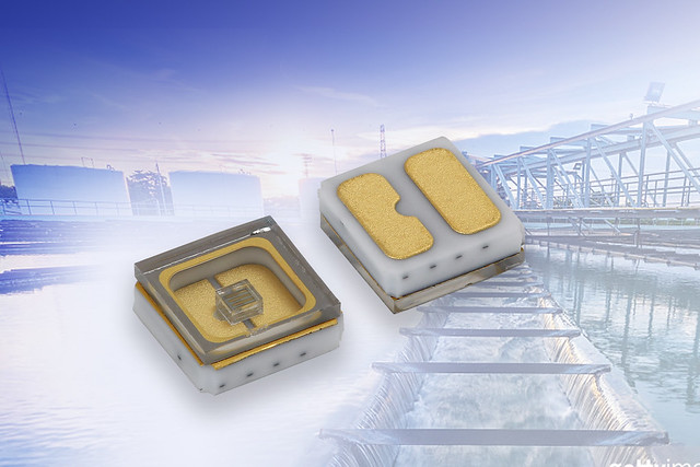
Devices Combine Typical Radiant Power of 37 mW With a Longer Service Life of 27 000 Hours and a Shorter Typical Wavelength of 274 nm for Higher Disinfection Efficiency.
Vishay Intertechnology, Inc. today introduced two new UVC (short wavelength ultraviolet) emitting diodes in a ceramic / quartz-based package for sterilization in medical, industrial, and consumer applications. Compared to previous-generation solutions, the Vishay Semiconductors VLMU35CR40-275-120 and VLMU35CR41-275-120 deliver higher radiant power at a lower cost, while offering higher disinfection efficiency and longer service life.
The devices released today feature high typical radiant power of 37 mW at 250 mA, which in terms of mW/$ performance is 30 % higher than lower power emitter diodes and 12x better than previous-generation solutions. In addition, the VLMU35CR41-275-120 provides a minimum radiant power of 30 mW at 250 mA, which is the same as the closest competing device at 350 mA.
Product Benefits:
Delivers an extremely long lifetime
Features a compact 3.5 mm by 3.5 mm by 1.2 mm surface-mount package with a quartz window
Emission angle of ± 60°
High radiant power to 3.2 mW at 20 mA or 7.5 mW at 50 mA
Maximum forward voltage of 6.5 V
Wavelength range of 265 nm to 285 nm
Forward current up to 70 mA
RoHS-compliant, halogen-free, and Vishay Green
Compatible with reflow soldering processes
Features a Moisture Sensitivity Level of 3 in accordance with
The emitter diodes offer a wavelength range of 265 nm to 280 nm, with a typical wavelength of 274 nm. Not only is this suitable for direct disinfection of surfaces, air, and static water, but compared to 280 nm solutions, the VLMU35CR40-275-120 and VLMU35CR41-275-120 deliver 20 % higher sterilization efficiency. Available in a compact, thermally optimized surface-mount 3.45 mm by 3.45 mm by 1.7 mm package with a ceramic substrate and quartz window, the devices ensure a long service life of 27 000 hours at 250 mA and 25 °C.
Built on AlGaN technology, the VLMU35CR40-275-120 and VLMU35CR41-275-120 are designed to replace low-pressure UVC mercury tubes, especially in compact designs where small components are required. Typical end products will include sterilization devices for ear buds, toothbrushes, water bottles, refrigerators, air purifiers, door handles, medical instruments, coffee machines, ATMs, toilet seats, vacuum cleaners, and more.
The devices feature DC forward current up to 300 mA, forward voltage down to 5.2 V, and an emission angle of ± 60°. RoHS-compliant, halogen-free, and Vishay Green, the VLMU35CR40-275-120 and VLMU35CR41-275-120 are compatible with reflow soldering processes and feature a Moisture Sensitivity Level of 3 in accordance with J-STD-020.
Samples and production quantities of the new UVC emitting diodes are available now, with lead times of eight to 16 weeks.
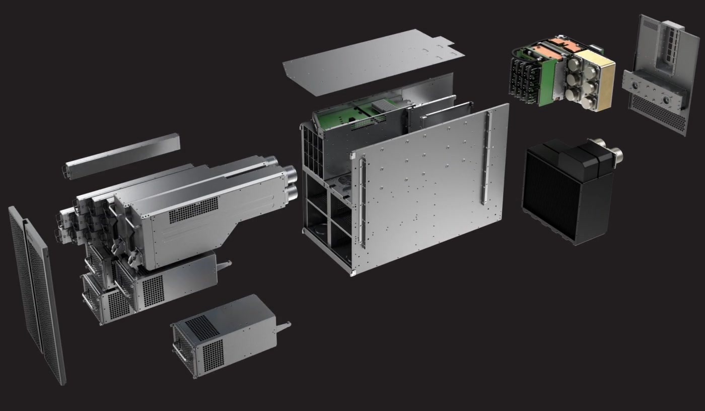
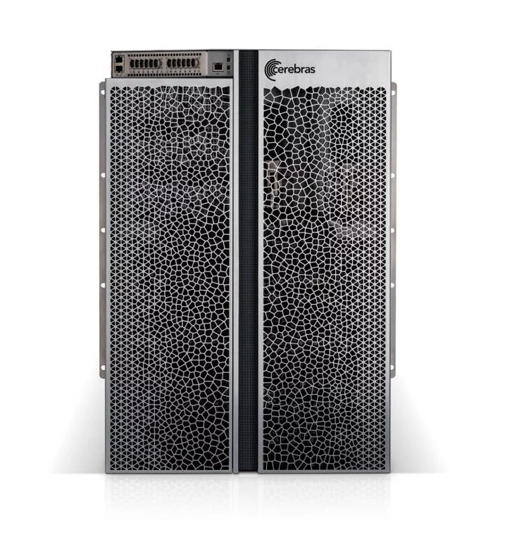
Cerebras Systems recently achieved an incredible milestone in the field of Artificial Intelligence (AI) model training. Cerebras announced the ability to train multi-billion parameter AI models on a single CS-2 system.
The Cerebras Systems claims to be able to train complex Natural Language Processing (NLP) models with up to 20 billion parameters on a single CS-2 System. Hence, reducing the system engineering time to train large AI models from months to minutes.
In NLP, the models trained on a larger amount of data perform more accurately than those trained on smaller datasets. Conventionally, the training of AI models involves the batch-processing approach. The batch-processing approach involves splitting up the data over a number of smaller processing units. Batch processing reduces the load on particular hardware and training time. However, the new record set by the Cerebras Systems enables the training of multi-billion parameter AI models on a single CS-2 System with enhanced computational speed.
As stated by Andrew Feldman, CEO, and Co-founder of Cerebras Systems, they are
“Proud to democratize access to GPT-3 1.3B, GPT-J 6B, GPT-3 13B, and GPT-NeoX 20B, enabling the entire AI ecosystem to set up large models in minutes and train them on a single CS-2”.
This engineering marvel is achieved by the amalgamation of the computational resources and small size of the Cerebras Wafer Scale Engine-2 (WSE-2) and the Weight Streaming software architecture enhancements made available by the Cerebras Software Platform, CSoft’s release of version R1.4. The Cerebras WSE-2 is one of the largest processors ever built. The computational resources of the WSE-2 enable the training of huge AI models without splitting the data over multiple GPUs.
Training Multi-Billion Parameter AI Models on a Single CS-2 System in Minutes
With the new Cerebras WSE-2, training of multi-billion parameter NLP models over a single CS-2 System is possible. The powerful WSE-2 along with the Weight Streaming software architecture enables the training and evaluation of huge AI models without the requirement of load distribution or batch processing over multiple GPUs. Moreover, it reduces the system engineering required from months to minutes. The Cerebras Systems’ WSE-2 is a revolution in the field of AI model training and evaluation.
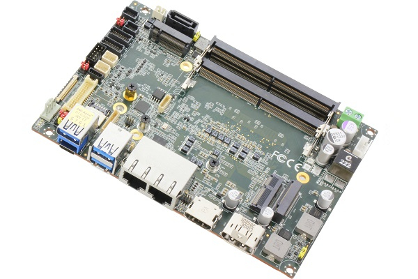
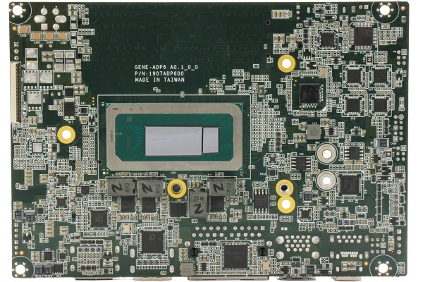
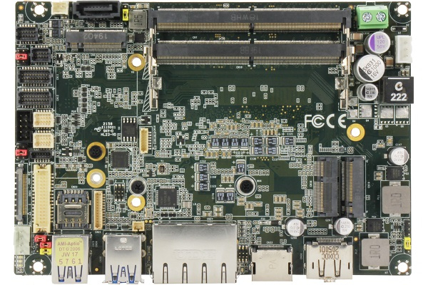
With a 15% boost in CPU performance, 50% faster data transfer speeds, and four independent displays with Intel Iris® Xe Graphics, the GENE-ADP6 is the perfect board for machine vision solutions.
AAEON’s new GENE-ADP6 unlocks the door to elite edge computing, digital signage, and machine vision applications with enhanced features across the board. The GENE-ADP6 provides a 15% improvement in CPU performance through the Intel® 12th Generation Core™/Celeron® CPU (formerly Alder Lake-P), featuring hybrid platform processor architectures with up to 12 cores and 16 threads.
Along with an improvement in CPU power, the GENE-ADP6 shows greater AI-readiness, with Intel’s Deep Learning Boost AI accelerator providing enhanced inferencing capabilities to make the GENE-ADP6 perfect for 5G and AI edge computing.
For faster, more advanced storage speeds, the GENE-ADP6 introduces 64GB system memory via two dual-channel DDR5 SODIMMs, being AAEON’s first 3.5″ SubCompact Board to do so. This improvement from DDR4 to DDR5 offers up to 50% faster data transfer speeds and a new, more efficient power management structure.
The GENE-ADP6 supports M.2 3052/3042 and M.2 2230 modules, enabling 5G and Wi-Fi for enhanced application connectivity. Additionally, the board’s FPC expansion slot provides sophisticated, high-performance PCIe x4 (Gen 4) speed. This also gives users the flexibility to expand the board’s additional PCIe x4 slot for machine vision, smart retail and industrial automation applications.
This is all supported by AAEON’s dense, yet intricate I/O featuring three USB 3.2 slots, four USB 2.0 slots, and a display interface for four independent displays with Intel Iris® Xe Graphics. It is this combination of features that AAEON believes will see the GENE-ADP6 become the foundation for more refined digital signage and machine vision solutions.
For more information about the GENE-ADP6, please visit our product page or contact the AAEON sales team.
The digital logic circuit whose output, at any instant, is dependent on its inputs only is referred to as a combinational logic circuit. The output state(s) of the combinational logic circuit is the logical result of the combination of its inputs and does not involve any kind of memory or storage etc. Contrary to this, the output(s) of a sequential logic circuit is dependent on inputs and the previous state(s) of output. The storage of the previous state of output acts as a memory in the sequential logic circuit and feedback also plays a similar role.
The combinational logic circuit has no memory, storage, feedback, etc. which could affect its logical output besides inputs. At any instant of time, the states of inputs are immediately reflected at the output depending on the logical combination of input states. This means that the output can change state from “0” to “1” or from “1” to “0” at the very moment the state of any input changes, accordingly.
Figure 1: The block diagram of a combinational logic circuit
Components of Combinational Logic Circuit
The combinational logic circuit consists of basic components such as logic gates, input, and output variables. The input and output variables represent digital states i.e. either “0” or “1”. Whereas, the logic gates form the combinational logic and may consist of NAND, NOR, and NOT logic gates. These logic gates are the basic building blocks of any digital logic circuit. The combination of two or more logic gates forms the combinational logic circuit. The NAND, and NOR logic gates, as discussed in the Logic Gates section, are termed “Universal Gates” as any other logical circuit can be constructed using only any of them. The combinational logic circuit can be simple or complex depending on the number of logic gates or logical operations it performs.
The task of a combinational logic circuit is to perform a defined logical function and there are multiple ways to specify a logical function. The function of a combinational logic circuit can be specified or expressed by the following methods:
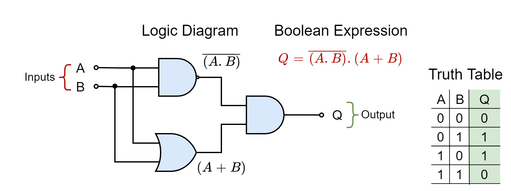
Truth Table
The Truth Table represents the logical function of a combinational logic circuit in tabular form which lists all of the possible combinations of inputs and their states against the respective output(s). Simply, it lists the logical output(s) for each of the possible combinations of its inputs.
Boolean Algebra
The Boolean Algebra expresses the combinational logic in the form of an expression or equation. The expression relates the input and output variables to produce the desired function or output. The expression can be evaluated by feeding the input states i.e. “0”s and “1”s and checking for the outcome against the input states.
Logic Diagram
The logic diagram is the graphical representation of the combinational logic circuit. It consists of logic gates wired together in a specific manner to perform the desired function. The logic diagram details each and every logic gate used in the combinational logic by using a specific graphical symbol of each gate.
Figure 2: The representation methods of combinational logic
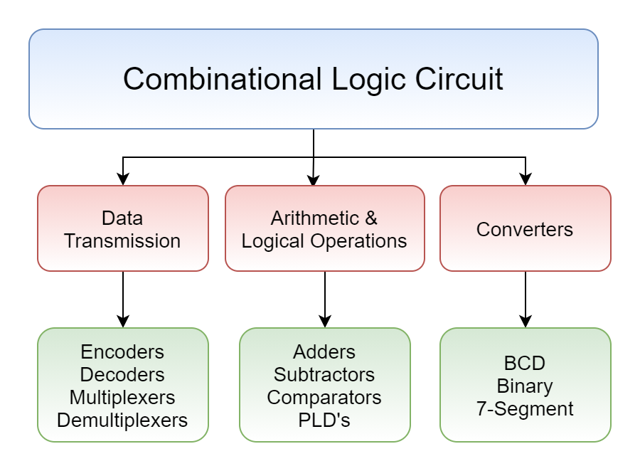
As said earlier, the combinational logic circuit consists of logic gates that are connected together in a combination to perform a specific function or decision, etc. The combinational logic circuit combines two or more input signals to produce at least a single output signal depending upon the logical operation it performs. The typical applications or functions performed by combinational logic circuits are Encoders, Decoders, Multiplexers,De-multiplexers, Adders, etc.
Classification of Combinational Logic
Figure 3: Applications of combinational logic circuits
Amongst the applications of combinational logic, the most important and widely used ones are multiplexer and de-multiplexer circuits. The multiplexers depending on the select lines, route one of the many inputs to a single output line. The select lines represent the code to select the input line which will be routed to the single output. As such, the select lines are decoded to identify the input to be routed. On the other hand, the de-multiplexer performs the reverse of the multiplexing, that is, it routes a single input to one of the many output lines depending on the select lines. The multiplexer consists of essentially two parts: decoder and solid-state switches. The application and working of the solid-state switches are described before discussing multiplexing, de-multiplexing, encoding, decoding, etc.
Solid-State Switches
Conventional electro-mechanical switches and relays are not used in digital systems mainly due to their high transition time. On the other hand, silicon-based solid-state switches have a fast transition time and they incur negligible losses. The Transistor-Transistor-Logic (TTL) based solid state switches use a transistor as a switch which is a unidirectional device. The field-effect-transistor (FET), Complementary-Metal-Oxide-Semiconductor (CMOS) based, devices act as bidirectional switches and are nearly perfect to be used in applications requiring bidirectional solid-state switches. The solid-state switches are commonly classified depending on the switching applications and have different types and ratings etc.
Switching Applications of Solid-State Switch
The three (3) main switching applications of a solid-state switch are listed below:
Analog Switches: They are used in routing signals such as audio, video, data switching/ communication, instrumentation and process signals, etc.
Digital Switches: They are involved in high-speed signal routing, data transmission, and performing switching in digital peripherals such as USB, LAN, USART, Ethernet, etc.
Power Switches: They are used in passing high voltage and current signals such as used in power supply modules, rectifiers, inverters, etc.
Analogue Bilateral Switches
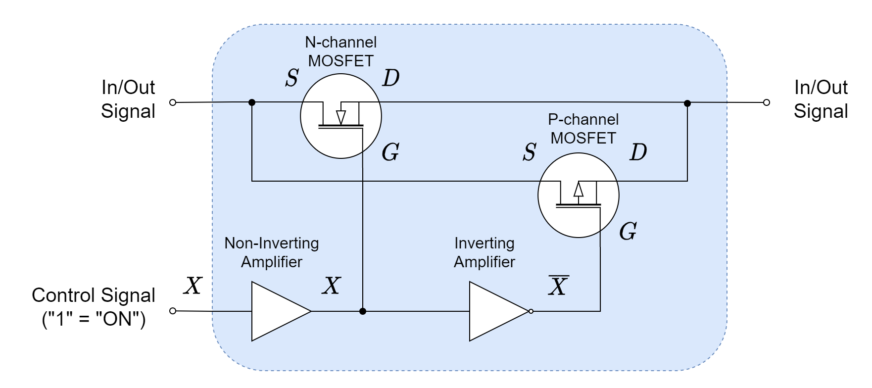
The analog bilateral switches are those which suppress (block) switching of data and signal currents when in the “OFF” state and allow the same when in the “ON” state only. The triggering of the switch state is carried out by a digital signal applied at the control gate of the switch. The switching, between “OFF” and “ON” and vice versa, is rapid. The switch offers a negligible resistance (ideally zero) in the “ON” state and very high resistance (ideally infinite) when it is “OFF”. In the following figure, a typical bidirectional solid-state switch consisting of N & P-channel MOSFETs is shown.
Figure 4: The typical diagram of bidirectional MOSFET-based switch
The direction of signal or data can switch from left to right or from right to left depending on the states of MOSFETs and the voltage level of both sides. The states of MOSFETs are triggered by the “Control” signal. When the “Control” signal is “1” then N-channel MOSFET is “OFF” and P-channel MOSFET is “ON”. The states of MOSFETs are reversed when the “Control” signal is “0”.
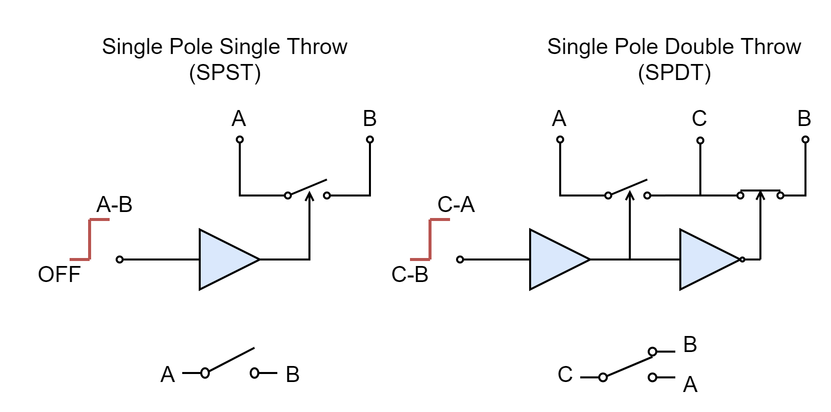
Types of Contact
Just like electro-mechanical switches, the solid-state switches are also termed according to the number of throws and poles each switch offers. For example, Single Pole Single Throw (SPST), Single Pole Double Throw (SPDT), Single Pole Quad Throw (SPQT), etc. The state of each contact is either “Open” or “Closed” and under normal conditions i.e. unenergized state they are standardized as “Normally Open (NO)” and “Normally Closed (NC)”, respectively. Moreover, they also include configurations such as make-before-break and break-before-make, etc.
In the following figure, a few contact types are illustrated.
Figure 5: The Single-Pole-Singe-Throw (SPST) and Single-Pole-Double-Throw (SPDT)
The analog switches are commercially available in the form of IC packages and each IC includes multiple switches to form multi-channel multiplexers. For example, the 74HC4066 has four (4) independent bidirectional switches. The commonly known multiplexer and demultiplexer have Multi-way Bilateral Switches which are variants of CMOS analog switches.
Conclusion
The digital circuit whose output is dependent on the combination of inputs only is called a combinational logic circuit.
The combinational logic circuit has no “memory”, “timing”, or “feedback”. There is no storage or role of the previous state(s) of output(s) in the determination of the next output state(s).
The output(s) of the combinational logic circuit changes in accordance with the inputs only, instantaneously.
The combinational logic circuit performs the function which can be specified or expressed by a truth table, Boolean expression, or a logic diagram.
The most common applications of combinational logic are multiplexers, demultiplexers, half adders, full adders, encoders, and decoders.
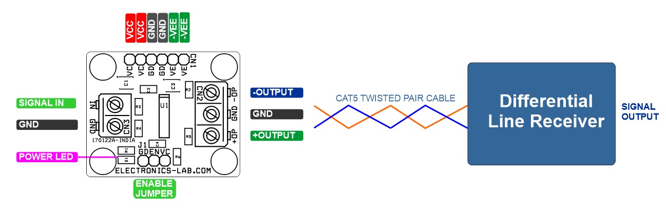
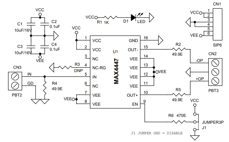
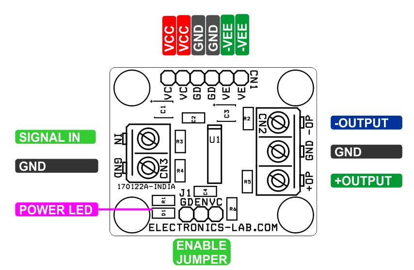
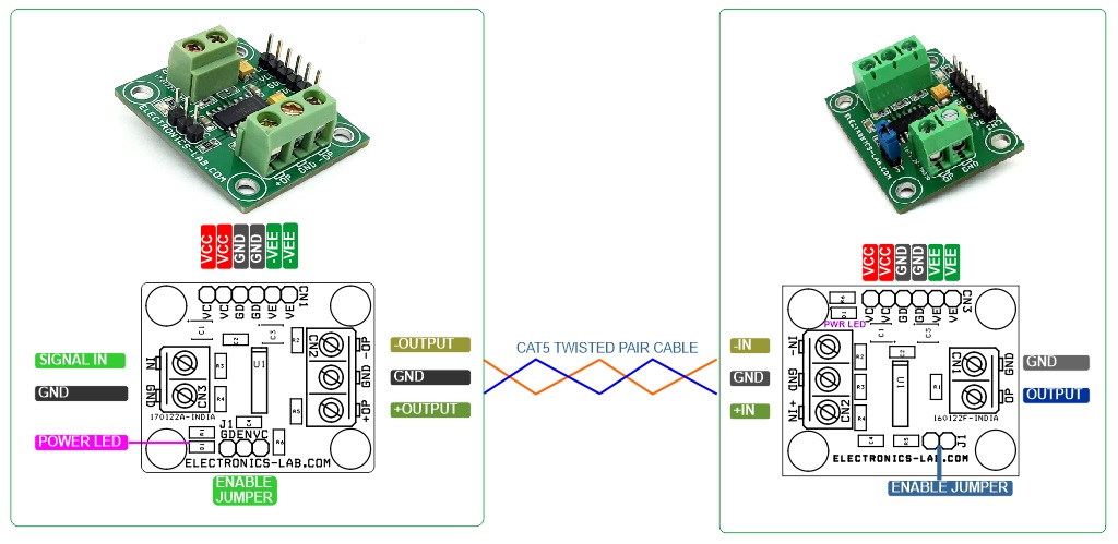
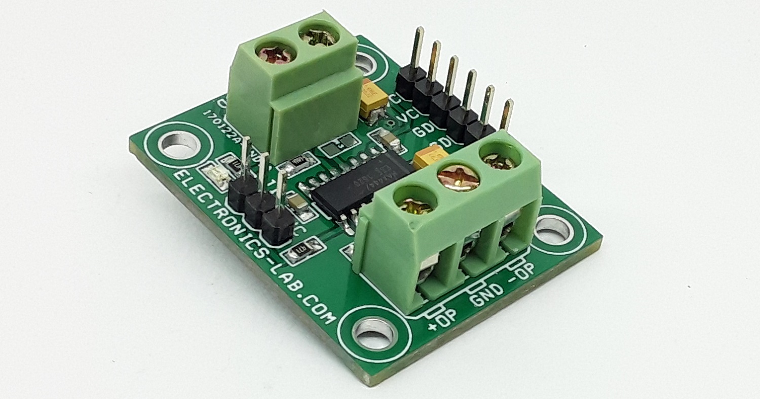
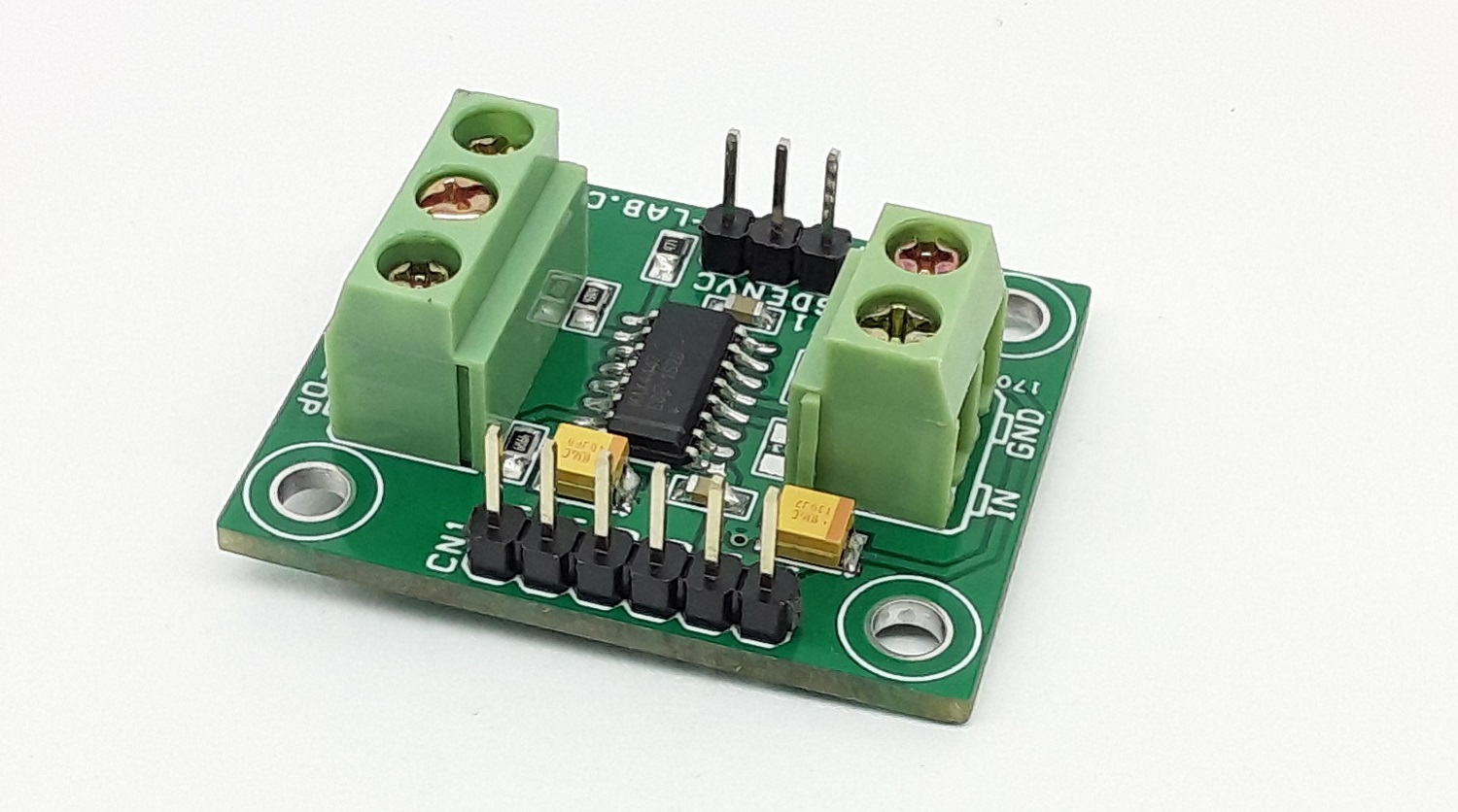
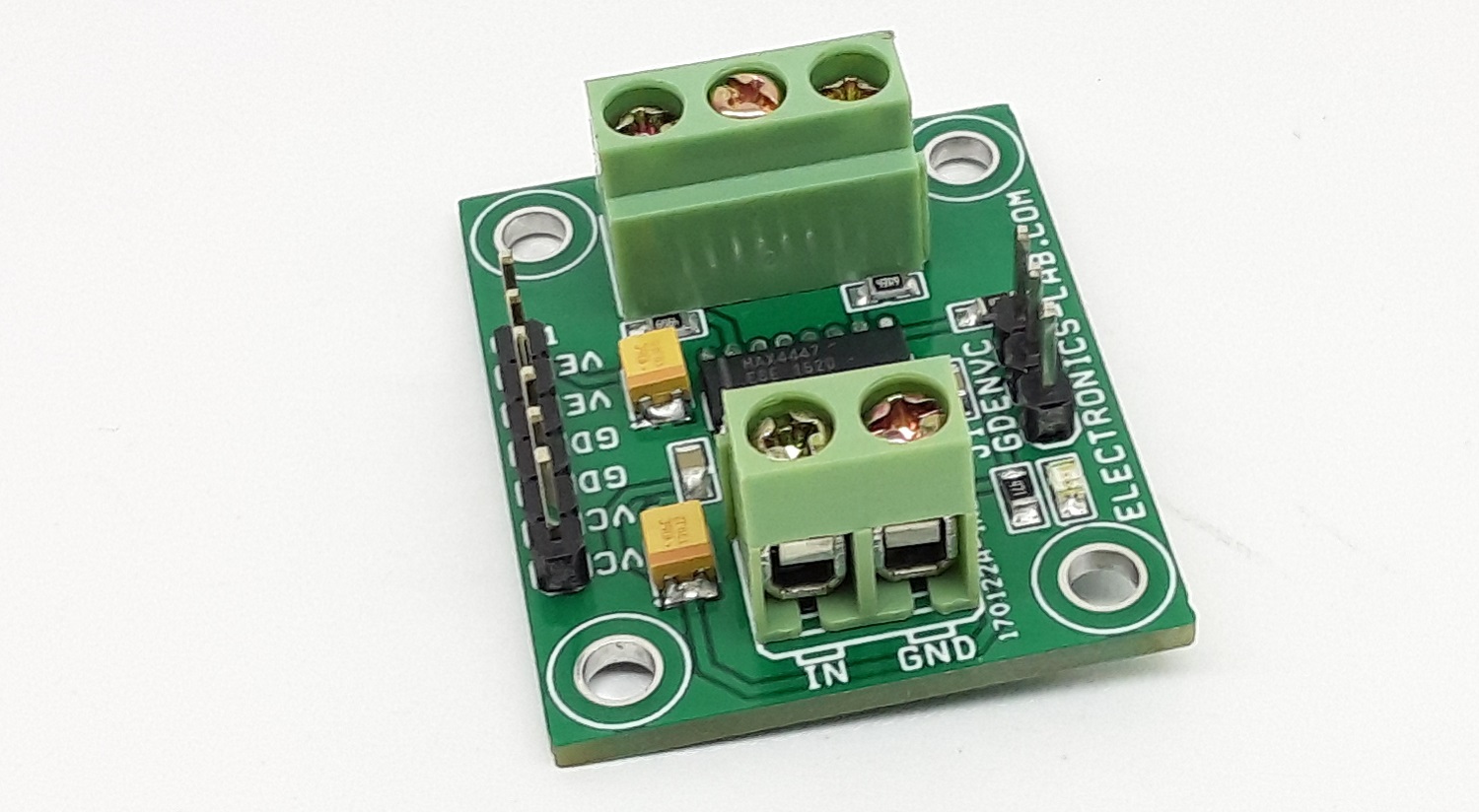
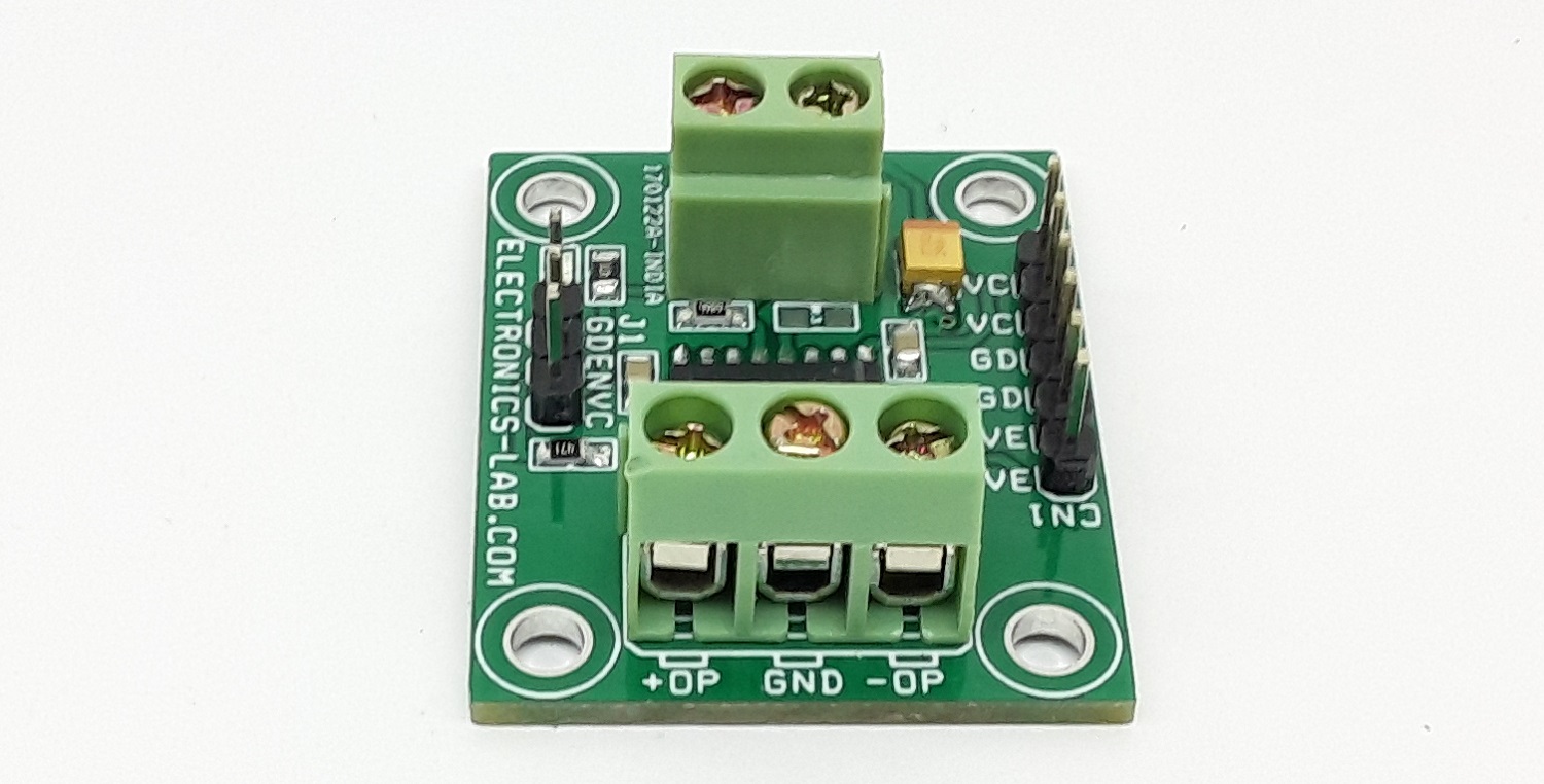
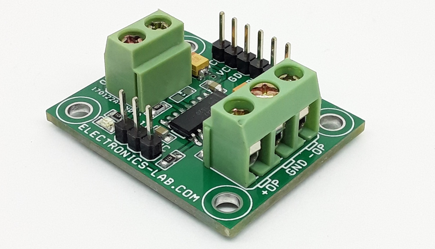
This is a Line Driver project. This single-ended-to-differential line driver is designed for high-speed communications. Using current feedback for greater bandwidth, this project delivers full-power bandwidth up to 405MHz and features slew rates as high as 6500V/µs. The MAX4447 has a fixed gain of +2V/V and a small-signal bandwidth of 430MHz. A low-power enable mode reduces current consumption below 5.5mA and places the outputs in a high-impedance state, Jumper J1 is provided to selectively enable and disable. The circuit can deliver differential output swings of ±6.2V from ±5V supplies with a 50Ω load. Excellent differential gain/phase and noise specifications make these project ideal for a wide variety of video and RF signal-processing and transmission applications. It is advisable to use gold-plated PCB and high-quality connectors for high-frequency operation.
The project is well-suited to drive twisted-pair cables. It is advisable to use a high-quality twisted pair cable like CAT5. The 24AWG telephone wire widely used, produces losses at higher frequencies.
Connections and Other details
CN1: Power Supply Input >> Pin1 =+5V DC, Pin2=+5V DC, Pin3=GND, Pin4=GND, Pin5= -5V DC, Pin6= -5V DC
CN3: Signal Ended Signal Input >> Pin1= Signal Input, Pin2=GND
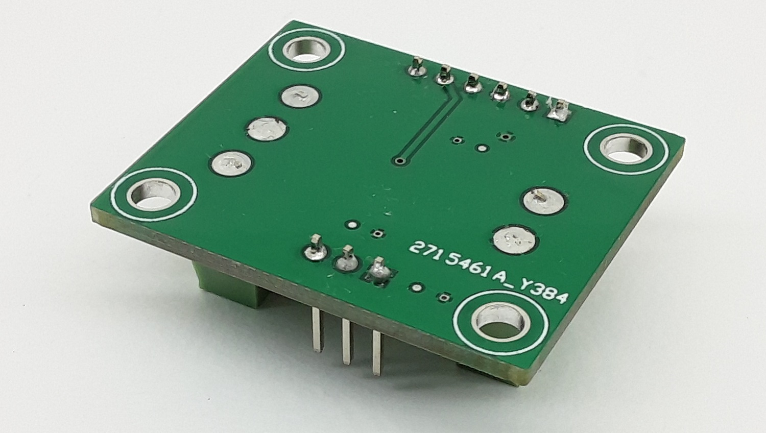
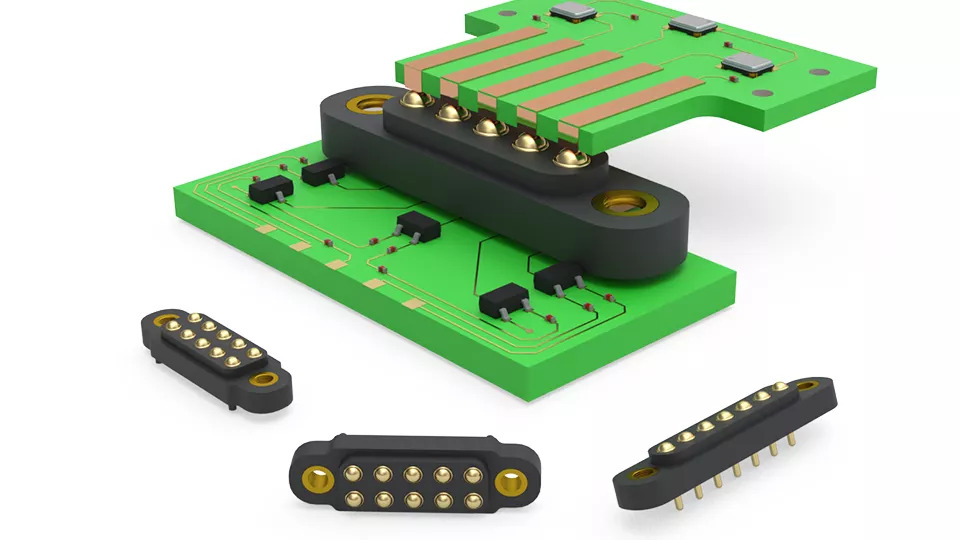
Introducing new Omniball® spring-loaded connectors for applications requiring multiple points of contact in sliding or rotational orientations. The unique Omniball® spring-loaded contact (patent pending) features a rolling ball interface, enabling contact to be made between components in axial and non-axial alignments. These versatile connectors facilitate creative solutions for innovative interconnect arrangements while providing optimal electrical, mechanical, and structural reliability.
The connectors utilize Omniball® contacts, spring-loaded pins in which the traditional plunger has been replaced by a gold-plated, brass ball. They are designed to optimize connections between components that slide or revolve into contact. When engaged, the ball compresses and rolls, allowing the mating surfaces to make contact and then easily slide parallel to each other while spring force acts to ensure consistent electrical contact is maintained. This rolling action prevents binding, premature wearing, and structural failure that traditional, plunger style, spring pin connectors can be prone to in these types of applications.
Omniball® connectors, offered in single and double row configurations, have a pin-to-pin spacing of 4 mm (.1575”), a .266” (6.76 mm) above board height, and are available in through-hole or surface mount termination styles. There are options for threaded inserts to provide secure mounting in rugged applications and for alignment pegs on the SMT connectors. Insulator material is Nylon 4/6, characterized by excellent high-temperature performance, dielectric strength, and mechanical toughness. Omniball® contacts feature .030” (.762 mm) maximum stroke, gold plating on all components, and a .091” (2.3 mm) diameter ball interface. These spring-loaded pins are durable, they have been tested to 1,000,000 compression cycles and rolled over 67 miles (108 km) at half stroke while still meeting specifications for contact resistance of 30 milliohms, and spring force of 55 grams at mid-stroke (.015”, .381 mm). Single row connectors are offered in 2-10 positions; part numbers are 845-22-0XX-10-0X1101 (through-hole) and 845-22-0XX-30-XX1101 (SMT). Double row connectors are offered in 4-20 positions; part numbers are 847-22-0XX-10-0X1101 (through-hole) and 847-22-0XX-30-XX1101 (SMT).
These new connectors are an excellent choice for any application that involves sliding or rotating connections, such as: “twist & lock” cable connectors; docking stations; rack and server drawers as well as quick connects and blind mating applications. They can be mounted in vertical or horizontal orientations and can be used to eliminate cables where circuit board to bus bar connections are made in tight spaces.
Need technical help or looking for a custom design? Use the form below to contact Mill-Max Technical Services.