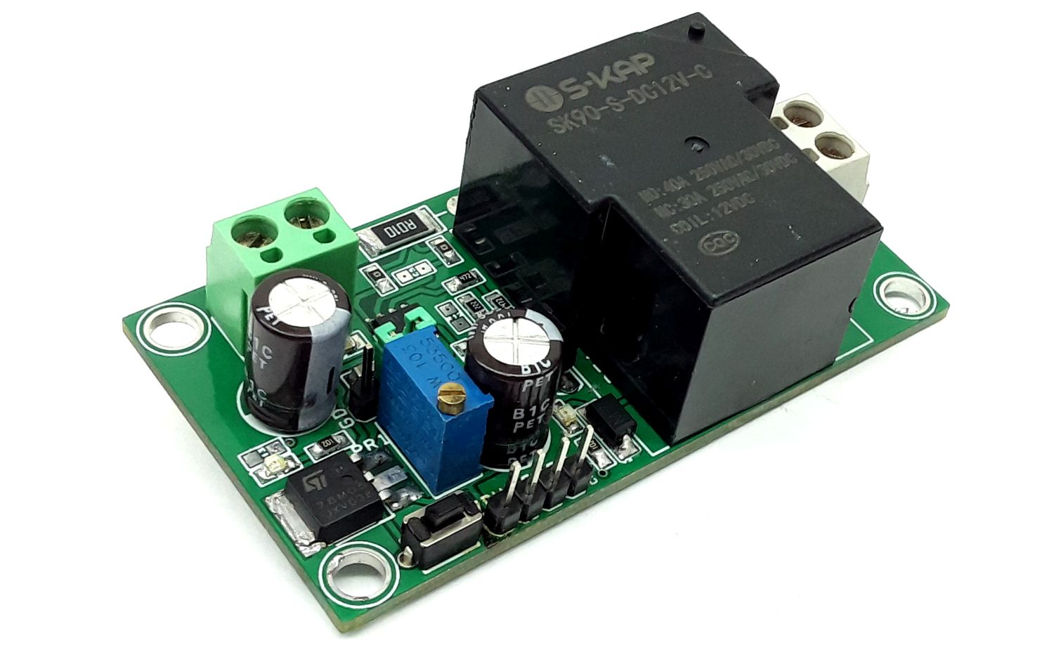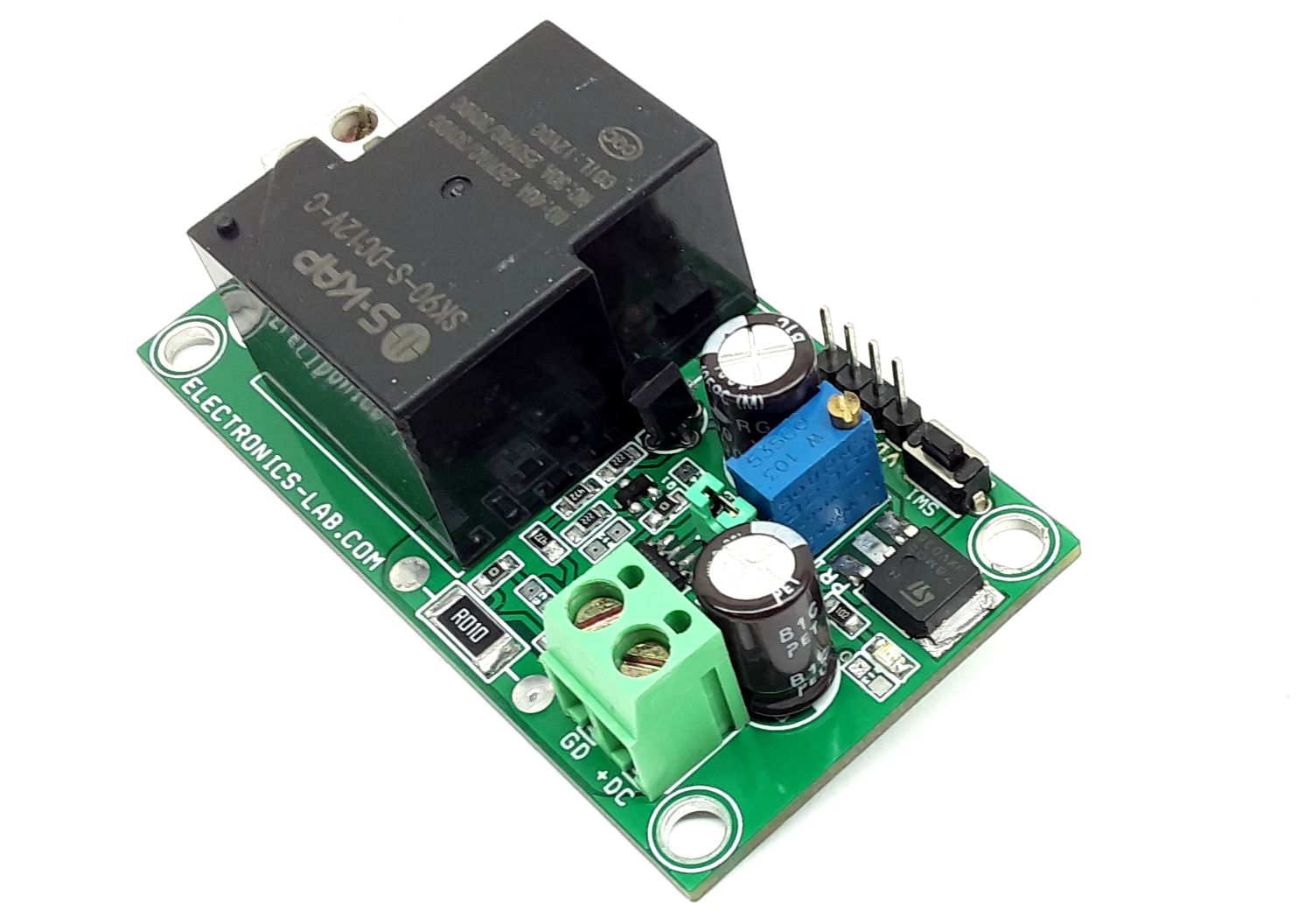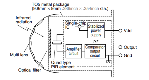
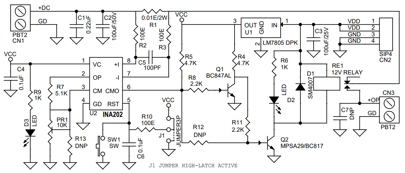
The project presented here is an over-current trip switch. It provides protection to a load when over current condition occurs. Basically, the project trips the relay when there is a short circuit or the load starts drawing much current. When the condition is favorable, press the tactile switch to power the load again. The threshold voltage of the comparator is 0.6V, the over-current limit can be adjusted using the trimmer Potentiometer PR1. Operating supply 12V DC @ 80mA when the relay is ON, load supply 0V to 48V.
The project is built using INA202 chip from Texas Instruments. The INA202 chip includes the high-side current-shunt monitor with voltage output and an integrated comparator. The device measures current through the shunt resistor R1 with current flowing in one direction that enables detection of an overcurrent event only when the differential input voltage exceeds the threshold limit. When the current reaches the set limit of the divider R7/ PR1, the output of CMPOUT transitions high, which turns Q1 on, pulls the base of the BJT transistor Q2 low which then switches OFF the relay, and turns the flow of the current OFF through relay contacts.
Trip Current Threshold
Trip current is adjustable from 250mA to 3A, PR1 trimmer potentiometer is provided to adjust the trip current, and load supply range is from 0 to 48V.
This project can be used for higher current trip and higher Voltage load with a few changes. Please refer to Datasheet for more details.
- Shunt Resistor R1 (Choose a lower value for higher current Trip), Maximum range 30A (Due to Relay Contacts Limit of 30A)
- R7 and PR1/Optional R13 Resistor Divider (Trip Voltage Threshold), Internal Reference Threshold 0.6V
- For Higher voltage up to 80V, Choose Capacitor C1 and C2 100V
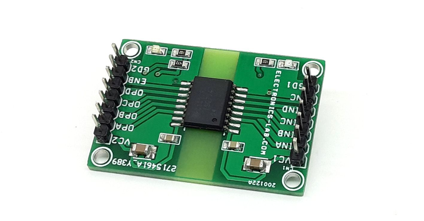
Connections and Other Details
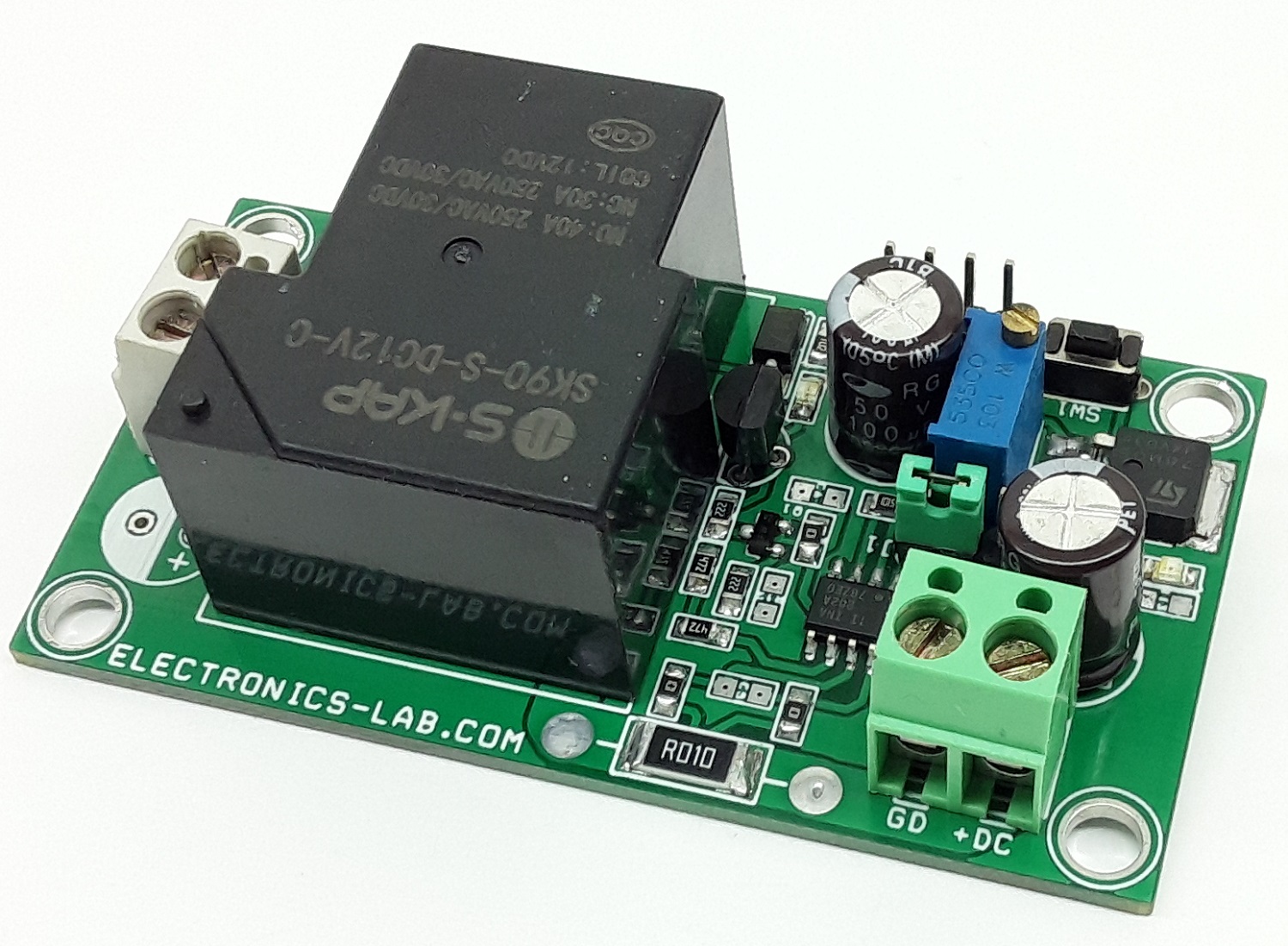
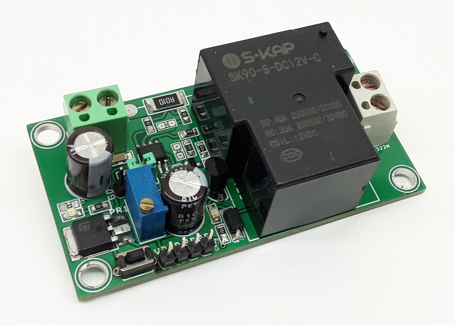
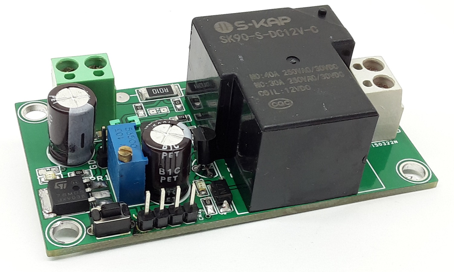
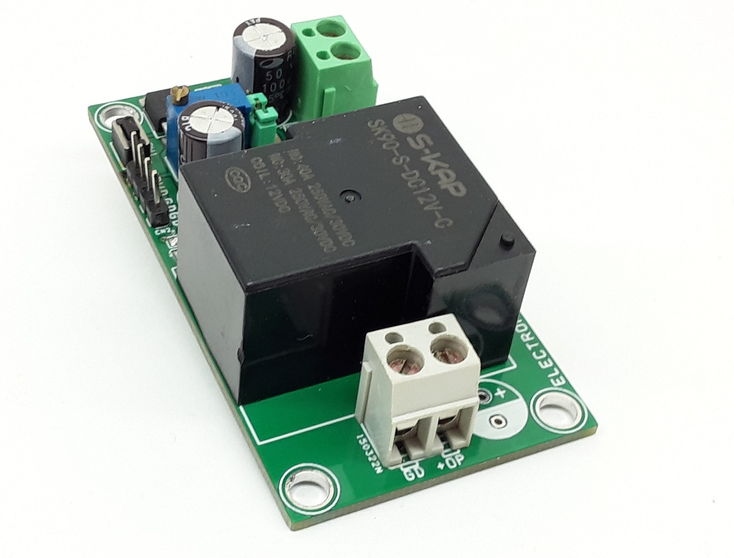
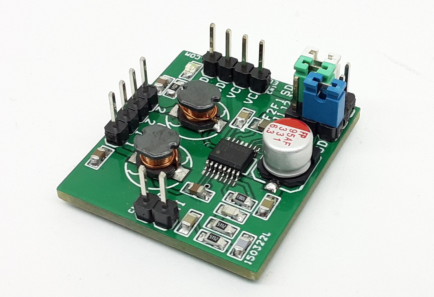
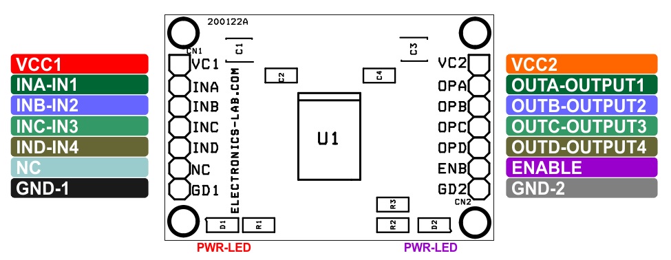
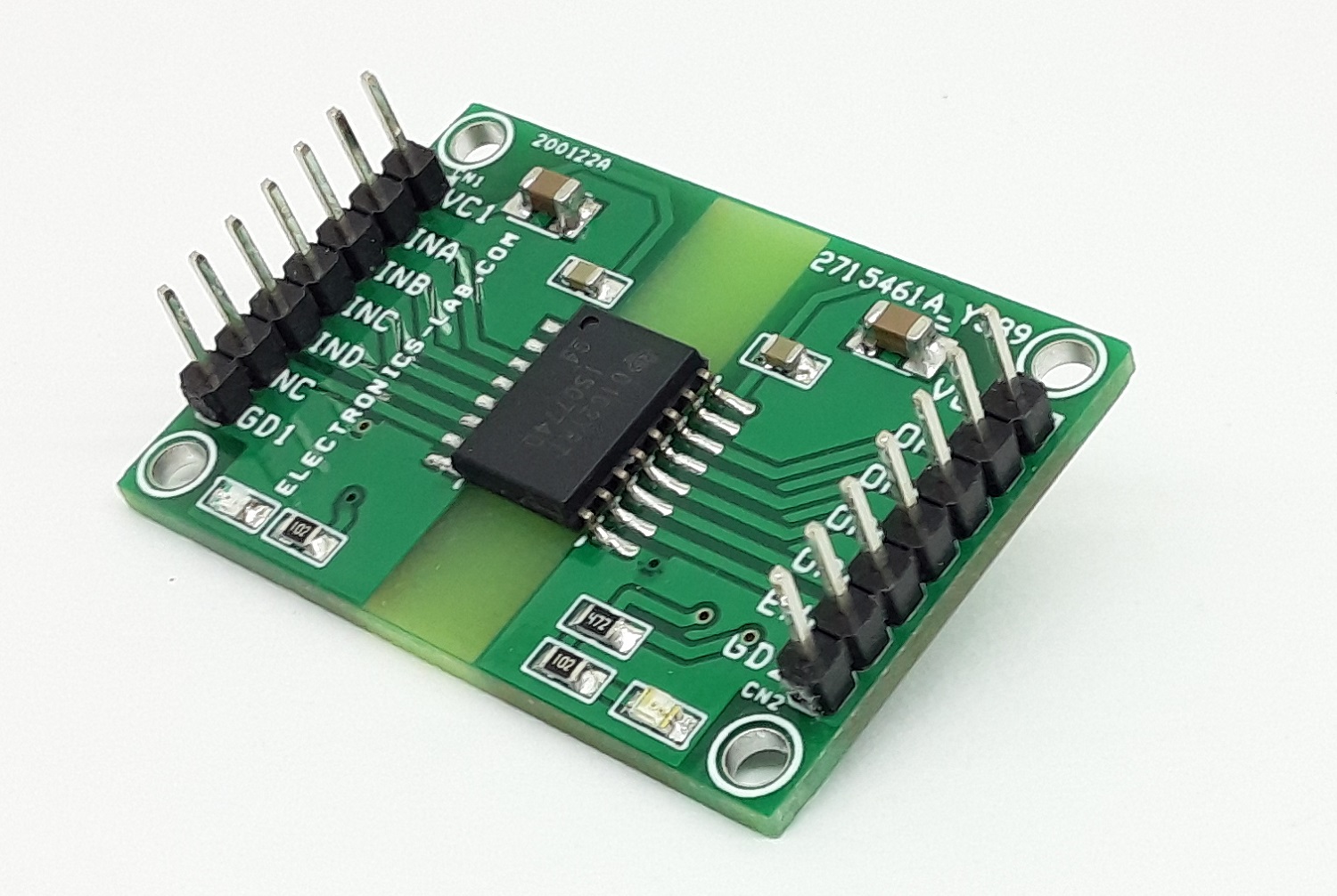
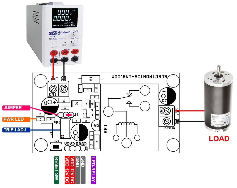
- CN1: Load Supply Input 0 to 48V DC, Current Up to 5 Amps (Pin 1 = + DC Input, Pin 2 = GND)
- CN3: Load Connection (Pin 1 = + DC Output, Pin 2 = GND)
- CN2: Logic Supply 12V DC @ 80mA (Pin 1 = VDD, Pin 2 = VDD, Pin 3 = GND, Pin 4 = GND)
- LED D3: Power LED
- LED D2: Function LED (LED On = Relay Function)
- Jumper J1: Latch or Non-Latch (Connect to VCC for Latch)
- PR1: Trip Current Adjust 250mA to 3Amps (Approx.)
Features
- Operating Supply 12V DC @ 80mA
- Load Supply 0 to 48V DC (Higher Voltage up to 80V Possible Read Note)
- Load Current Trip Range 250mA to 3Amps Approx.
- Power LED and Function LED
- Screw Terminals for Load Supply and Load
- Header Connector for Load Switch
- Trimmer Potentiometer for Trip Threshold Adjust
- 4 x 4 mm Mounting Holes
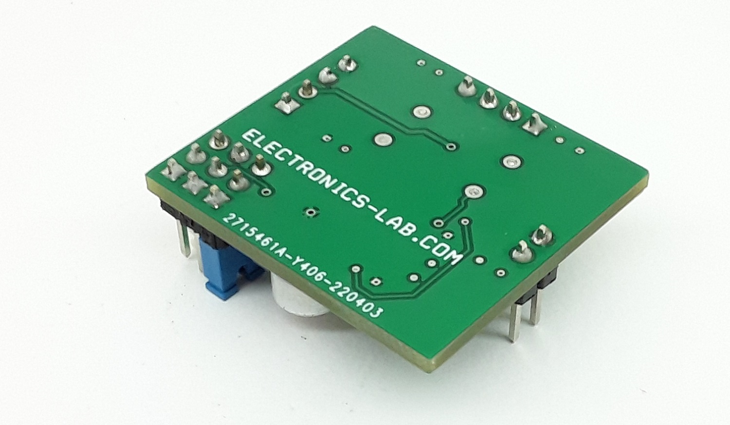
- PCB Dimensions 71.12 x 37.94mm
Schematic
Parts List
| NO | QNTY. | REF. | DESC. | MANUFACTURER | SUPPLIER | PART NO |
|---|---|---|---|---|---|---|
| 1 | 2 | CN1,CN3 | 2 PIN SCREW TERMINAL PITCH 2.54MM | PHOENIX | DIGIKEY | 277-1247-ND |
| 2 | 1 | CN2 | 4 PIN MALE HEADER PITCH 2.54MM | WURTH | DIGIKEY | 732-5317-ND |
| 3 | 1 | C1 | 0.22uF/50V SMD SIZE 1206 | YAGEO/MURATA | DIGIKEY | |
| 4 | 1 | C2 | 100uF/50V | NICHICON | DIGIKEY | 493-4508-1-ND |
| 5 | 1 | C3 | 100uF/50V OR 100uF/25V | NICHICON | DIGIKEY | 493-4508-1-ND |
| 6 | 2 | C4,C6 | 0.1uF/50V SMD SIZE 0805 | YAGEO/MURATA | DIGIKEY | |
| 7 | 1 | C5 | 100PF/50V SMD SIZE 0805 | YAGEO/MURATA | DIGIKEY | |
| 8 | 3 | C7,R12,R13 | DNP | |||
| 9 | 1 | D1 | SM4007 | SMC DIODE | DIGIKEY | 1655-1N4007FLCT-ND |
| 10 | 2 | D2,D3 | LED RED SMD SIZE 0805 | LITE ON INC | DIGIKEY | 160-1427-1-ND |
| 11 | 1 | J1 | 3 PIN MALE HEADER PITCH 2.54MM | WURTH | DIGIKEY | 732-5316-ND |
| 12 | 1 | PR1 | 10K MULTI-TURN TRIMMER POT | BOURNS | DIGIKEY | 3296Y-103LF-ND |
| 13 | 1 | Q1 | BC847AL | INFINION | DIGIKEY | BC847BE6327HTSA1CT-ND |
| 14 | 1 | Q2 | MPSA29 OR (BC817-CHECK PIN CONFIGRATION) | ONSEMI | DIGIKEY | MPSA29-ND |
| 15 | 1 | RE1 | 12V/30A RELAY | CIT RELAY | DIGIKEY | 2449-L115F11CM12VDCS.9-ND |
| 16 | 1 | R1 | 0.01E/2W SMD SIZE 2512 | VISHAY DALE | DIGIKEY | 541-WSL2512R0100FTA18CT-ND |
| 17 | 3 | R2,R3,R10 | 100E 5% SMD SIZE 0805 | YAGEO/MURATA | DIGIKEY | |
| 18 | 2 | R4,R5 | 4.7K 5% SMD SIZE 0805 | YAGEO/MURATA | DIGIKEY | |
| 19 | 2 | R6,R9 | 1K 5% SMD SIZE 0805 | YAGEO/MURATA | DIGIKEY | |
| 20 | 1 | R7 | 5.1K 1% SMD SIZE 0805 | YAGEO/MURATA | DIGIKEY | |
| 21 | 2 | R8,R11 | 2.2K 5% SMD SIZE 0805 | YAGEO/MURATA | DIGIKEY | |
| 22 | 1 | SW1 | TACTILE SWITCH | TACTILE SWITH | DIGIKEY | EG2510-ND |
| 23 | 1 | U1 | LM7805 DPK | ONSEMI | DIGIKEY | MC78M15ABDTRKGOSCT-ND |
| 24 | 1 | U2 | INA202 | TI | DIGIKEY | 296-INA202AID-ND |
| 25 | 1 | J1-S | SHUNT FOR JUMPER | SULLIN CONNECTOR | DIGIKEY | S9001-ND |
Connections
Gerber View
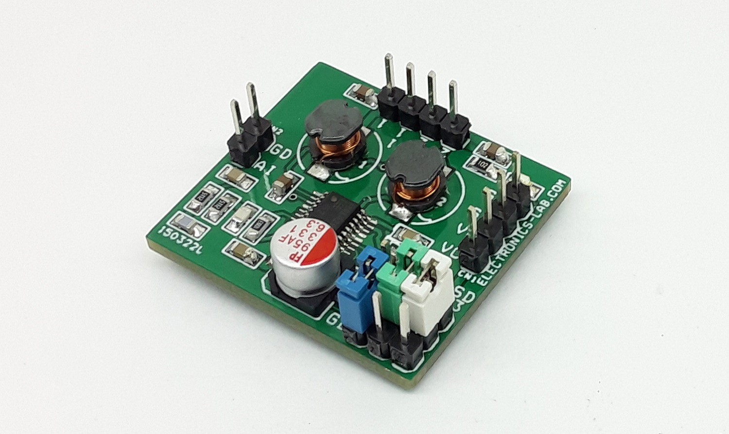
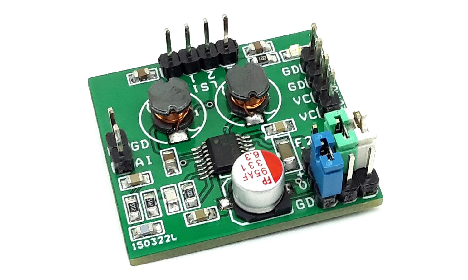
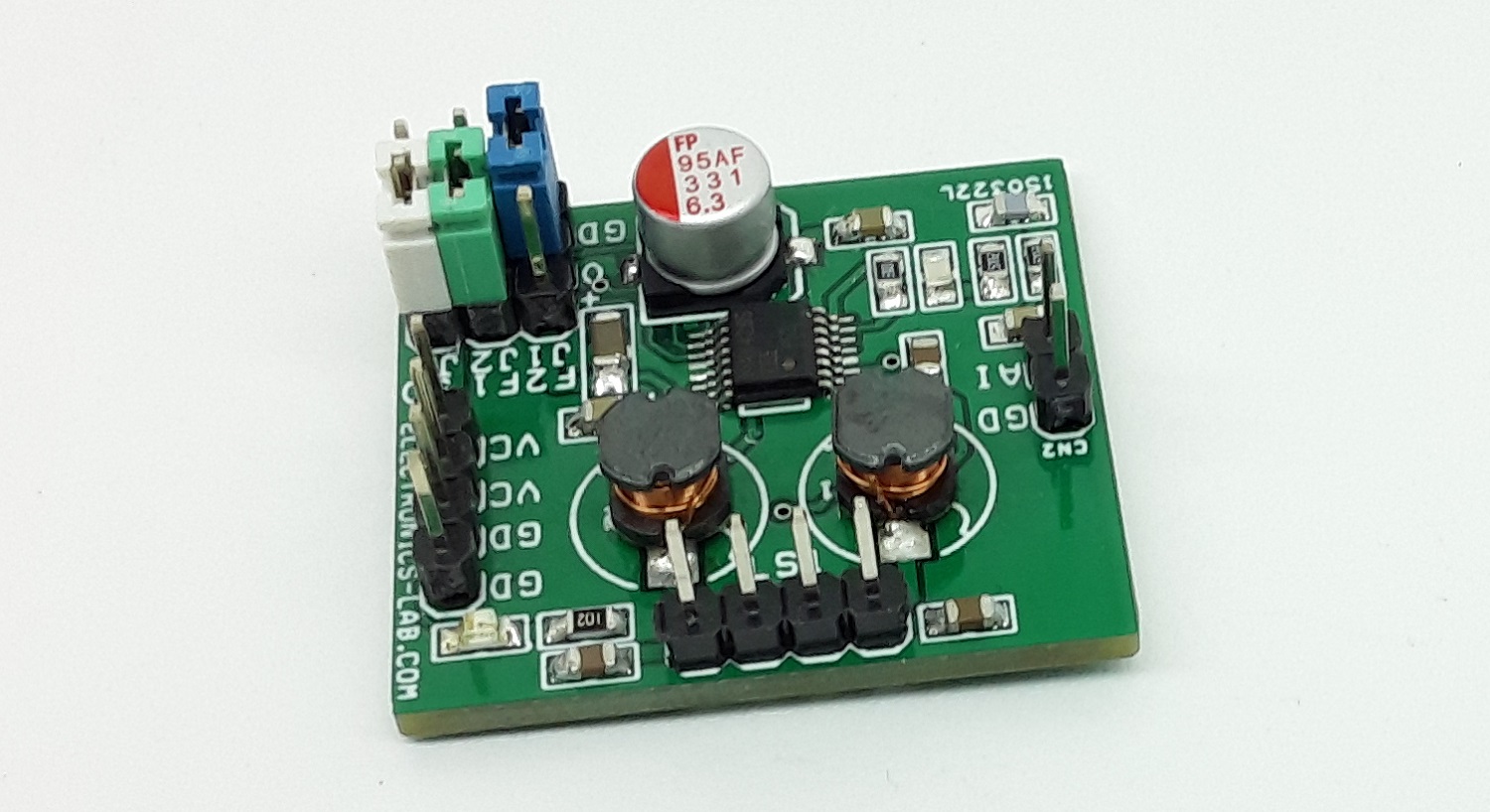
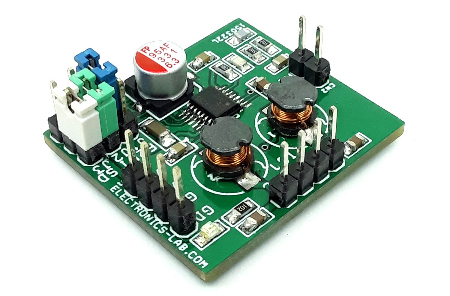
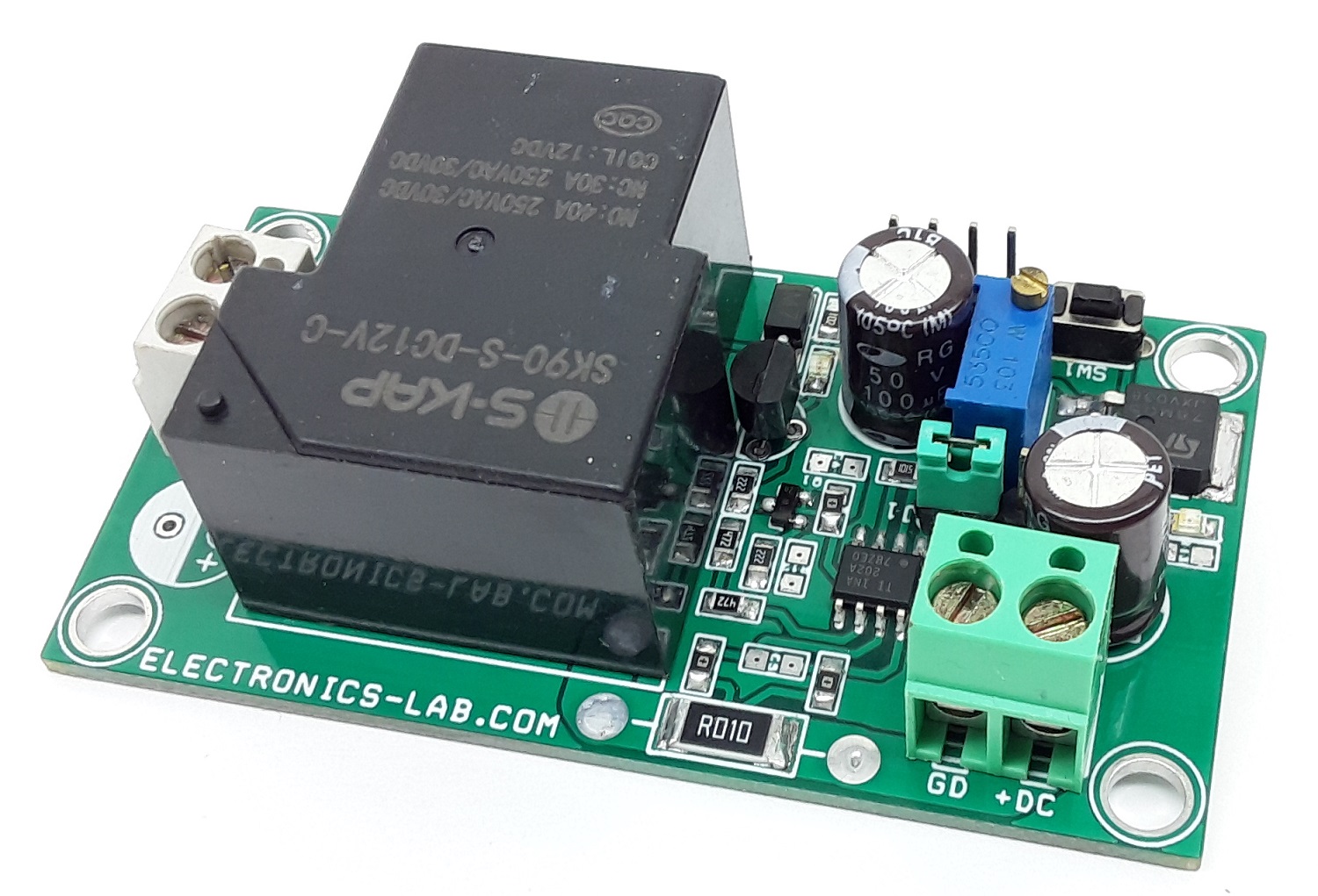
Photos