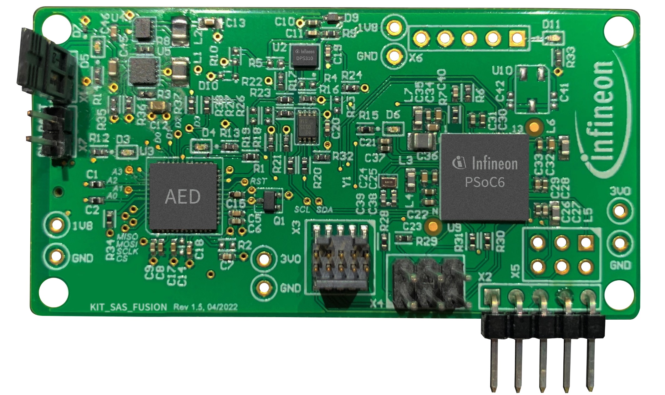
We recently witnessed the market position of Infineon in the embedded systems with the integration of its CYW43439 wireless chip into the very famous Pico family, Raspberry Pi Pico W microcontroller board. The company recently announced a battery-powered Smart Alarm System, which is a sensor fusion based on artificial intelligence and machine learning. The technology of low-power wake-on acoustic event detection provides high performance for smart builds and homes while achieving greater battery life compared to complex IoT solutions.
Infineon’s advanced security system is based on the company’s sensor fusion powered by the PSoC and XENSIV sensors. The combined technology of Infineon’s multi-layered security system that uses XENSIV microphones and XENSIV barometric pressure sensor with acoustic event detection provides the sensor fusion algorithms running on PSoC a protection and monitoring features against burglary and intruders.
“We are excited to enable a unique and differentiated approach to bring AI/ML capabilities to cost-sensitive, battery-powered home security sensor systems, without sacrificing battery life,” said Laurent Remont, Vice President of IoT and Sensor Solutions at Infineon’s Power & Sensor Systems Division.
The home alarm system needs to be robust and should not be triggered by other household sounds or background noises to avoid false alarms. Infineon Smart Alarm System supports three events that the technology can protect against– glass breaks, intruders, smoke detectors, and carbon monoxide detectors. For all the specific applications, the system is capable of understanding the intensities in the frequency spectrum, avoiding false alarms and providing greater accuracy.
The proposed alarm system incorporates the company’s signal-to-noise ratio analog XENSIV MEMS microphone, XENSIV digital pressure sensor, and a PSoC 62 microcontroller. The system also provides sensor fusion algorithms used to precisely train tinyML models to combine acoustic and pressure sensor data for accurate detection. With increased accuracy, AI models are able to eliminate background sounds that usually generate false positives.
“Current home security solutions are unreliable for detecting events such as glass breaks. Our new solution combines a number of best-in-class technologies to create an alarm system that is smart, reliable and power-efficient. We look forward to bringing more innovative solutions into the home security market.”
Alarm system reference design technology is available today, while the board will be available later this fall starting in September 2022.
JLCPCB for faster electronics manufacturing, carrying out its new standard PCB assembly service as an ace project created by JLCPCB, has been committed to reducing PCB assembly costs, improving ordering experience, speed up SMT lead-time, therefore, it gives the hand for professional electronics engineers to focus on their electronics business which allows industrial companies to manufacture high-quality electronics product.
Although the SMT project of JLCPCB was officially launched in 2019, the foundation of the entire project started in 2006, and it has been stable for 16 years. JLCPCB is good at summarizing SMT industry standards. The components angle is an industry problem that plagues SMT. JLCPCB was one of the first companies to stand out and popularize the standard. The latest IPC-7351C may also adopt this standard.
The electronics industry people involved getting to say “…”
Procurement staff: I can’t source complete parts
Electronics Engineers: JLCPCB helps me to save time and cost. I have more time available for validating scenarios.
Factory workers: Entire production line will arrange orders on the production line efficiently.
Entrepreneur: JLCPCB helps me to improve my business through time and cost-saving
How does the Global Parts Sourcing service greatly save time and money?
Building up parts lib by JLCPCB parts pre-order service (launched in 2021) and parts global sourcing service (launched in 2022) is PCB assembly technology innovation. Welding of more than 100 pieces has always been painful and difficult for the PCB manufacturing industry, this causes chip manufacturers to be unwilling or refused to provide such services for various reasons. JLCPCB pioneer another shortcut invests huge sums of money, and creatively adopts no replacement individual feeder models to cure SMT sample production pain. Sufficient-components SMT service for JLCPCB’s new and forward-looking global parts sourcing service is on its self-developed and one-stop platform build up supply amid the global parts shortage problem which allows people to prepare parts in advance. Knowing
there is a keen demand for components hinders the industry’s development. JLCPCB launches a global sourcing service in order to expand the parts supplying source for our customers, such a decision will provide customers with high-quality authentic components more stably, allowing them to achieve self-sufficiency on the JLCPCB SMT platform.
Compare to buy-as-you-go mode, pre-order parts allow people to get a favorable price. Pre-order service adopts real-time quotation service, and the price is transparent and open. JLCPCB does not earn any price difference, and also implements a policy of multiple refunds and multiple supplements for pre-purchased components. Customers can purchase on-demand without worrying about the loss of payment due to the failure of the pre-order service. JLCPCB is able to obtain more low-cost but high-quality parts from reliable global parts suppliers. And we know that component agents or original components will have corresponding purchase prices. In order to protect
their own interests, MOQ is a common method used by component suppliers. The bargaining power of JLCPCB can help small and medium-sized enterprises or individual customers reduce cost risks, collect various component needs, and negotiate prices with trusted component suppliers
first to obtain more favorable prices and to save customers money and effort.
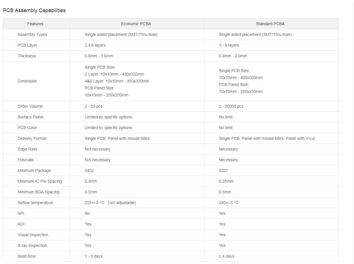
What’s the newest 1-6 layer double-side Assembly
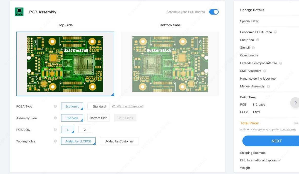
JLCPCB newest standard PCB assembly service allows SMT batch production and double-sides soldering of boards (patch + plug-in). No limit on PCB quantity, no limit on PCB process, no limit on parts kinds, V -cut panelization.
Standard PCBA service is more cost-effective
Assembly fee: $0.0017 per joint
Setup fee:$8 (JLCPCB $54 New User coupon free your setup fee)
Stencil Fee: Free
Example: There are 5 boards that require SMT, each with 200 solder joints, total: 10 solder joints assembly fee + Setup fee:$8 + $0 Stencil Fee
Standardized independent online ordering mode, real-time quotation of patch order, real-time display of patch effect, what you see is what you get, and short ordering process that you can master safely. In this era, disturbing users as little as possible in the pursuit of a good product.
Why is JLCPCB Standard PCBA Service faster easier cheaper?
JLCPCB integrated 4 major departments to improve SMT at full speed The 4: PCB, component, the stencil, and SMT are in the same industrial zone. Compare to other companies, JLCPCB transfer components, stencils, and SMT expressly, saving a lot of time through the AGV in the zone.
In order to ensure the most extreme SMT experience, JLCPCB Group also established a special working team for SMT lead-time and packaging in mid-March 2022. All businesses must take SMT as the highest priority.
JLCPCB Economic PCBA
JLCPCB Standard PCBA:
Quality-assured Standard PCBA service is faster and easier
The PCB stencil components are all self-operated, and they are all in the same production zone. This is the cornerstone to ensuring the quality, delivery time, and price of JLCPCB Assembly. Meanwhile by streamlining the entire process from ordering, parts sourcing and PCBA prototyping, you can get your products in hands as fast as one week. Allowing you to iterate, improve
and deliver on time or even faster:
Easier Ordering for Standard PCBA
Ordering process:
Place an order for PCB (circuit board)
Place an SMT (SMD) order
Payment
Production
QC
Shipping
What materials do you need to prepare?
Components: You don’t need to provide it, JLCPCB provides the required components
PCB (Circuit Board): Use PCB order
What documents do you need to prepare? GERBER+BOM+CPL
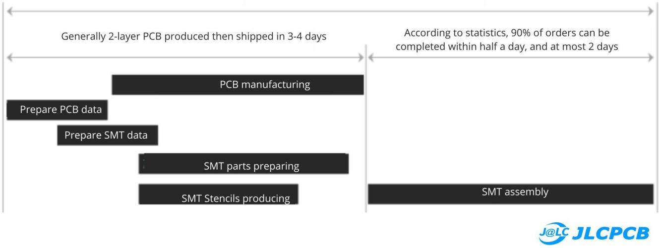
90% of SMT orders only take half a day of production
We deeply think about the effectiveness of our offered services, that’s why every single second counts, because the faster we go the more effective we become, through this equation, we could offer more reliable service to our customers. So we started thinking about the execution of the simultaneous task while producing the PCBs Assembly supporting lines are also getting ready simultaneously, such as components preparing, SMT stencils preparing. So, the overall construction period becomes shorter.
The following figure exemplifies the construction period of a 2-layer board:
Free $54 New User Coupon for Standard PCBA with 10M+ parts
Free $54 New User Coupon offered
Standard PCB Assembly supports double-side soldering, and unlimited quantity, order as many as you want
JLCPCB SMT Parts Library 200k+ in-stock components (689 Basic components and 200k+ Extended components); and 10M+ global parts
10M+ parts from reliable parts suppliers worldwide
Parts Pre-Order service from Global Reliable Parts Suppliers
Build Personal library Inventory, Save parts for current or future orders
How does JLCPCB keep Superior SMT quality by 6 self-operated industrial zones?
JLCPCB owns 6 Self-operated factories with high-end equipment quality process double-sided patch with plug-in wave soldering. Advanced Yamaha automatic placement machines and all equipped with electric mast, 10 temperature zone lead-free reflow soldering, automatic printing machine, mature and reliable management team, and self-developed supporting software. All LDI production equipment is used, with high precision, and there will be no line offset and assembly welding alignment offset. The four-layer board adopts LDI equipment, and the double-layer board adopts LDI+ automatic exposure machine equipment. JLCPCB only uses A-grade raw material
board, and never adopts less cloth, high filler, and non-flame retardant board. JLCPCB 4-layer PCB are all made of grade A-boards from real Taiwan Nanya and KB material, with real materials, and the price is around $72 / ㎡ ; The double-sided panels are all made of “true A-grade” boards, around $45.74 / ㎡.
“What you see is what you get” by free DFM checking
JLCPCB Free DFM file Checking offered a 3D simulation map of physical objects. After manual matching, you can see the patch effect from what you see and what you get. And one key Get a $54 New User Coupon. A special value-added service with a $24 SMT coupon every month.
After the matching, we will output a report (PDF can be exported in the upper right corner). Customers can use this PDF report for their project documentation and then they can determine the components that JLCPCB does not have and the components that can be pasted. Purchasing staff can search for missing materials offline and this will accelerate the process.
One-click alignment to solve the problem of components deviating from the pad. Due to incorrect automatic data processing or mismatch of component polarity, the loaded components sometimes deviate from the pad Taiyuan. At this time, manual adjustment is very time-consuming. In order to solve this problem, we provide a one-click adjustment:
For example, your design looks:
Press the Auto-Align button on the toolbar to automatically align all components:
Does JLC PCB Assembly make progress in the Electronics Industry?
Absolutely! JLCPCB PCB Assembly sincerely helps electronics engineers stay healthy. Manual welding is time-consuming and labor-intensive, with a high error rate, and is the number one killer of health, lung disease, and blindness. You should quickly order from who will help you solder common components, and let your PCBA boards are ready to use, in an industrial-grade quality.JLCPCB Standard PCB Assembly service produces PCBA in double sides (patch + plug-in). You can get assembled boards as quickly as 7 days. The standard PCBA production line equipment is also adjusted, such as automatic solder paste printing machine, SPI (solder paste inspection), AOI, and other equipment to better ensure product quality which helps the electronic industry and electronic business make progress. Get 54 New User Coupon to redeem a unique double-side PCBA journey now!
The Octal numbering system is another digital numbering system that uses the Base-8 system like the previously discussed Hexadecimal numbering system having the Base-16 system. The Oct- is a combining form used as a prefix meaning “eight” and that is why Base-8 (eight) system is termed an Octal numbering system. Likewise the Hexadecimal number, the octal numbering system reduces the size of an equivalent large binary number and makes it convenient to read and write to the original large binary number.
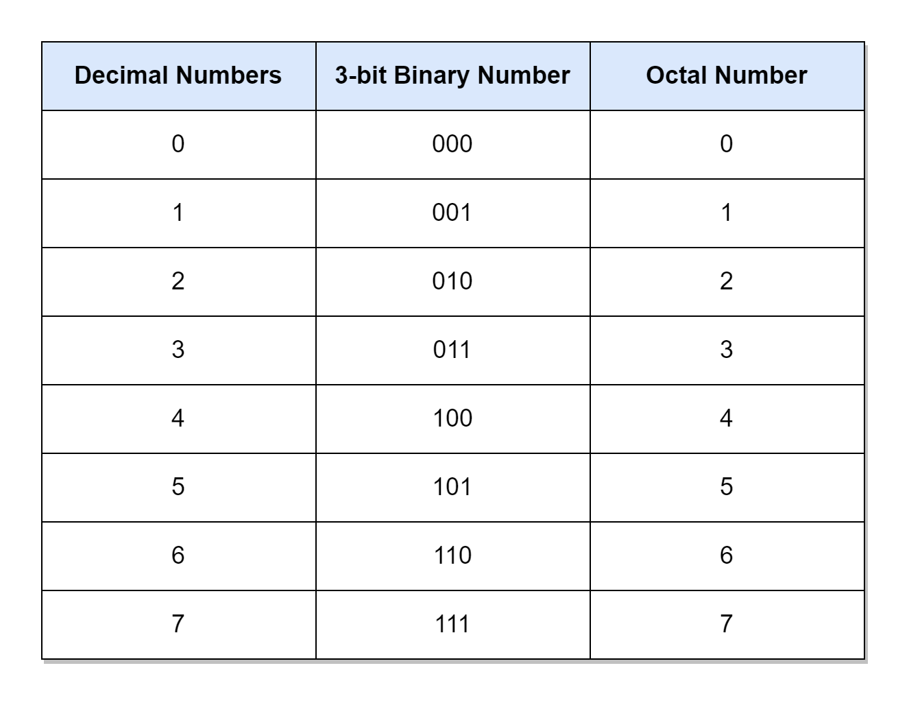
A numbering system’s digit has a range of numbers that it can use to express its value. This range is dependent on the base value of the numbering system i.e. Base-10 (decimal), Base-16 (Hexadecimal), or Base-8 (Octal), etc. For example, Base-10 and Base-16 systems have ranges of “10” and “16” numbers, respectively. Similarly, Base-8 (Octal) numbering system has a range of only “8” numbers from “0” to “7” i.e. 0, 1, 2, 3, 4, 5, 6, and 7. The octal numbers have only eight (8) distinct values for each digit and each digit has a weight of eight (8) starting from the least significant digit (LSD). In order to accommodate and express “8” numbers in binary, only three (3) bits are required. Following this, the octal values (0, 1, 2, 3, 4, 5, 6, and 7) corresponds to binary equivalent values (000, 001, 010, 011, 100, 101, 110, and 111), respectively.
The octal number is formed by grouping binary numbers in sets of 3-bits. It follows the same procedure adopted, previously, in the Hexadecimal article. However, in Hexadecimal numbers, a binary number was segregated into groups of 4-bits (as Base-16 uses the “0” to “15” range and requires 4-bits). The Octal numbering system is simple compared to the Hexadecimal numbering system as it uses only numbers compared to Hexadecimal using numbers plus alphabets. Moreover, it has only eight “8” distinct values compared to Hexadecimal’s sixteen “16” distinct values. In the early era of digital computing, the octal numbering system was very famous as digital inputs (D0 to D7) and outputs (Q0 to Q7) were in counts of eight (8). However, with the increase in the number of digital inputs and outputs, system architecture and memory size, etc. the hexadecimal numbering system has become more convenient for representing large binary values.
Representation of an Octal Number
The octal numbering system uses the Base-8 system and, as such, an octal number is represented by a subscript “8”. For example, the (1428) is identified as an octal number as it has a subscript of “8”. Further, it is noticeable that each digit of an octal number has a value between 0 and 7. For example, an octal number (1288) is wrong as its least significant digit (LSD) has a value of “8”. Which does not belong to the octal numbering range rather it belongs to the decimal or hexadecimal numbering system. So, a number can be identified to be correct by checking its base value and whether the number of each digit falls within its base range.
Octal Numbers
The following table lists the decimal numbers from 0 to 7 against their equivalents in binary and octal numbers.
Counting in Octal
Each digit of the octal number has a weight of eight (8) starting from the least significant digit. The weight of each digit increases by the power of eight moving from least significant digit to most significant digit. The equivalent weight in decimal of each octal digit, up to the 7th digit, is given.
The octal digit has a number range from “0 to “7” and, for counting above this range, another octal digit is added to the left. The addition of the second digit leads to the counting up to (778) which is, in decimal, equivalent to (6310). So, two octal digits can count up to 63. Similarly, a three-digit octal number can count up to (7778) which gives a counting range up to (51110) in decimal.
Addition of 0’s to a Binary Number
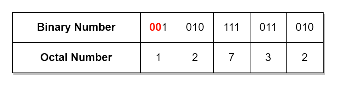
As the binary number is split into 3-bit groups in order to determine its equivalent octal number. This requires a binary number consisting of bits that are multiples of three (3) e.g. 3, 6, 9, 12, and 15, etc. However, this may not be the case when dealing with binary numbers and binary numbers can vary in bit lengths. The solution is to start splitting binary numbers, in groups of 3-bits, from the least significant bit (LSB). In case, the bits of the binary number are not equally divided amongst 3-bit groups then we will be left with less than 3-bits at the end. The leading zeros are added to leftover bits in order to extend their length up to 3-bits. This last group of 3-bits constitutes the most significant digit (MSD) of octal number. In the following table, a non-standard 13-bit binary number (1 0101 1101 101010) is converted to a 15-bit (divisible by 3) binary number by adding leading zeros, and then its equivalent octal number is determined.
In the above example, a 13-bit number requires 2-bits having zero values to be added to the left-most side in order to make it a 15-bit binary number. Similarly, an 11-bit binary number would require one (1) zero bit to be added. The usage of octal numbers reduces the length of binary numbers by three (3) times.
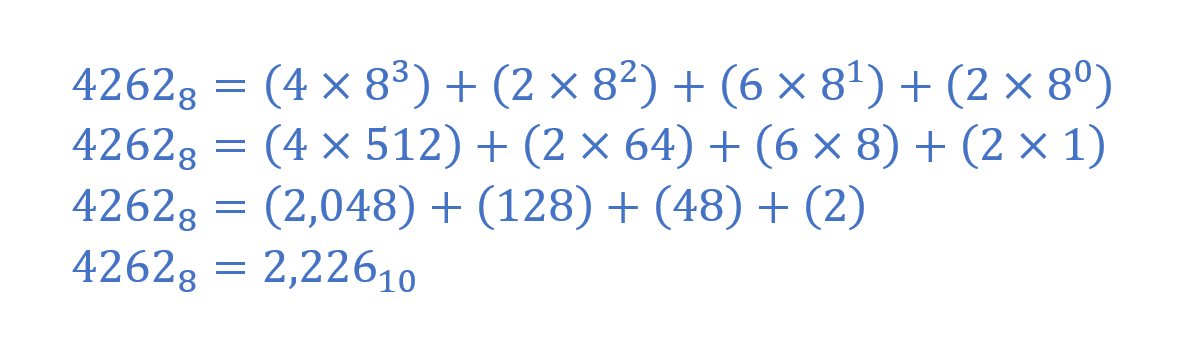
Octal to Decimal Conversion
The conversion of octal to decimal value is achieved by using the weighted sum of digits method described in the previous articles. In the following example, an octal number (42628) is converted to a decimal number.
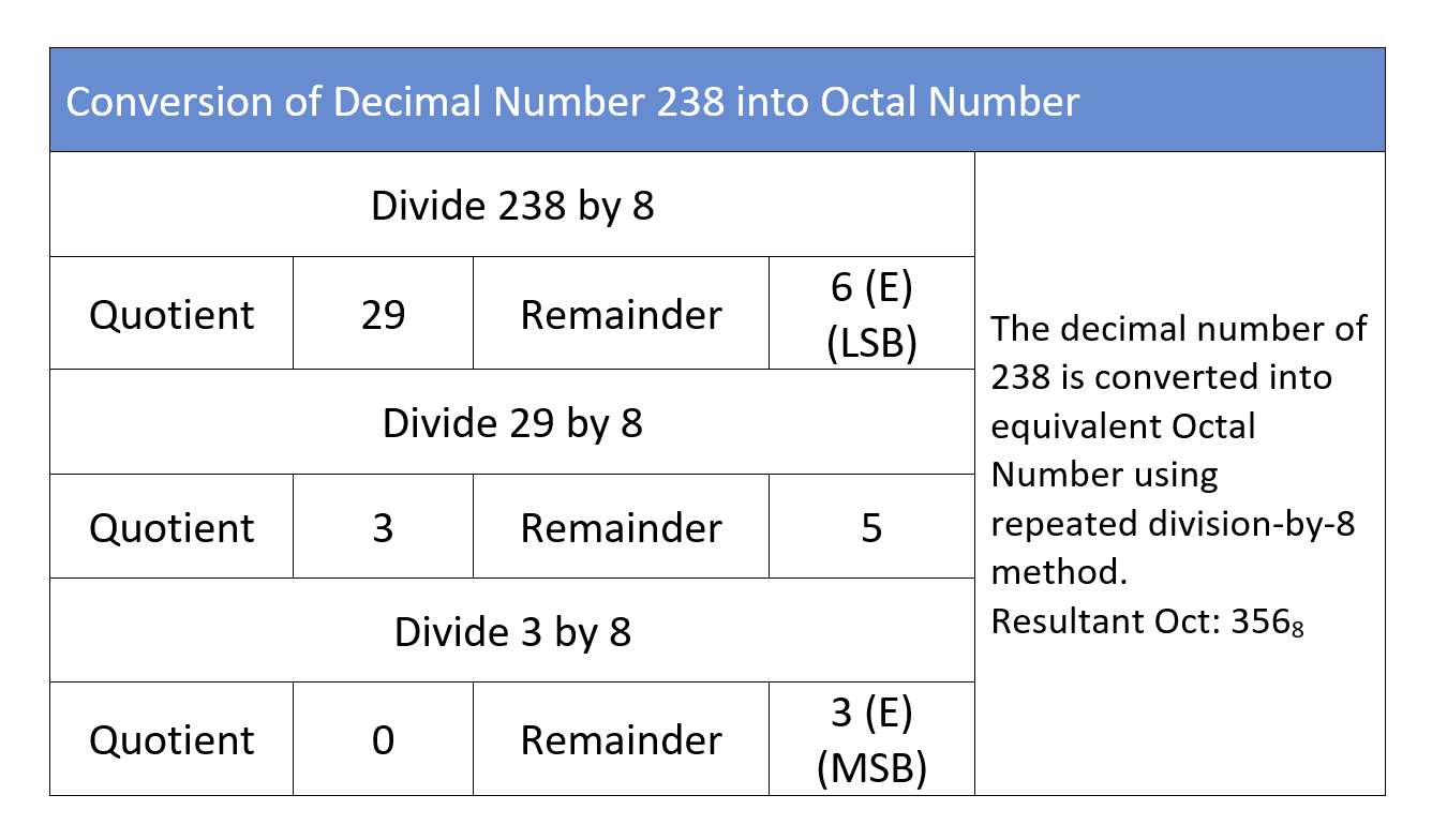
Decimal to Octal Conversion
The conversion from decimal to octal requires the application of the repeated-division-by-8 method. The same method was used to convert a decimal number to its equivalent binary and hexadecimal values in the previous articles. The decimal number (23810) is, hereby again, used to obtain its equivalent octal number in the following example.
Binary to Octal Conversion Example
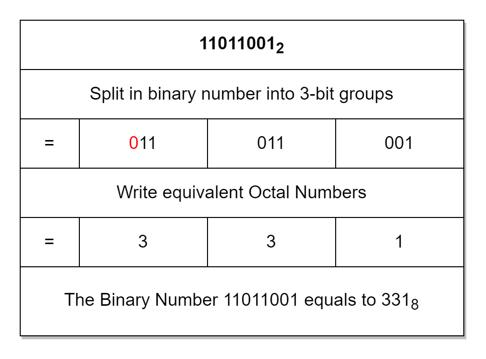
The conversion of an 8-bit binary number (110110012) to an octal number is illustrated below.
Octal to Binary and Decimal Conversion Example
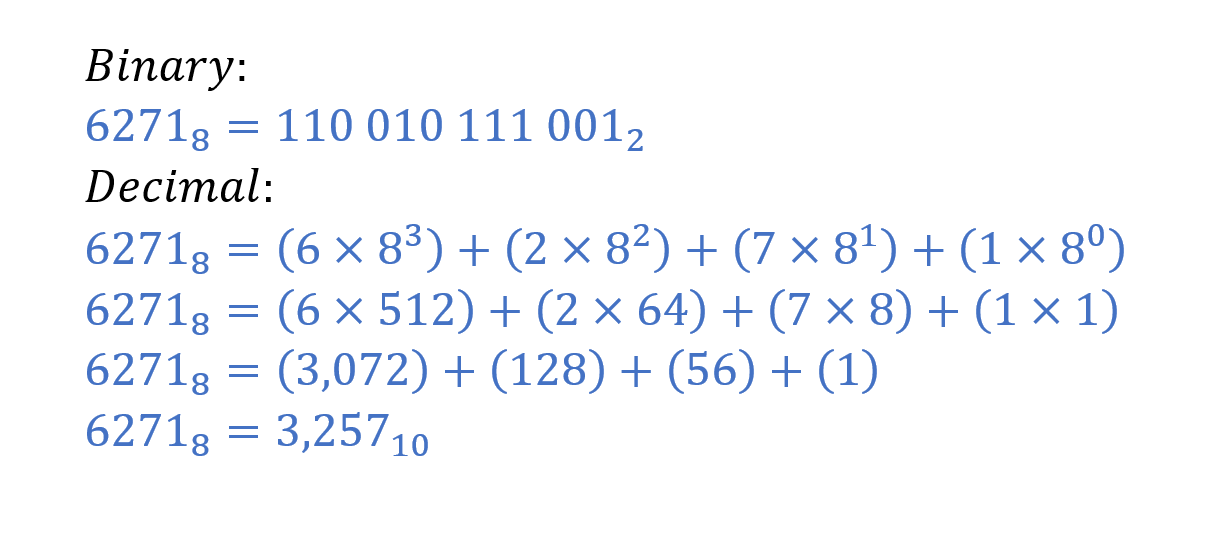
The conversion of (62718) to its equivalent binary and the decimal number is illustrated below as an example.
Conclusion
The Octal number uses a base-8 system and each digit’s value ranges from 0 to 7 i.e. eight (8) numbers.
In an Octal number, each digit is a group or set of 3 bits. The equivalent of a binary number in octal is obtained by splitting the binary number into 3-bit groups and an equivalent Octal value from “0” to “7” is assigned to each group.
The binary numbers may require the addition of leading zeros on the left most (most significant) side in order to form 3-bit groups.
The Octal number is represented by using “8” as a subscript e.g. 7358.
The Octal number can be converted to a decimal number by using the weighted sum of digits method.
The conversion from decimal to octal requires the application of the repeated-division-by-8 method.
The Octal number reduces the length of its equivalent binary number by a factor of three (3). However, octal numbers are seldom used now, and, as previously discussed, the hexadecimal numbering system has taken its place.
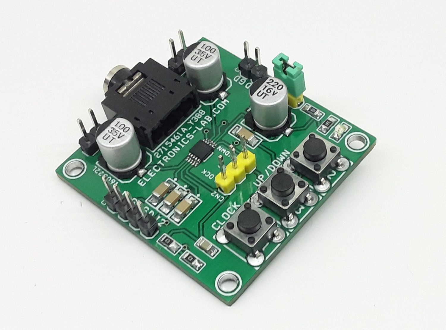
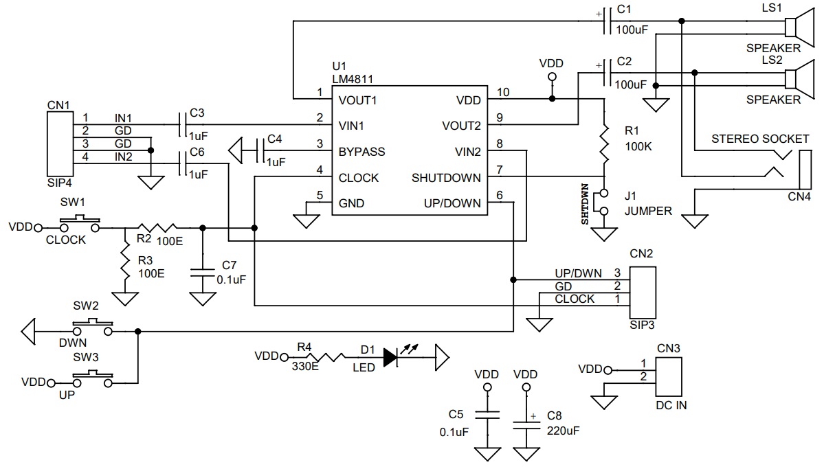
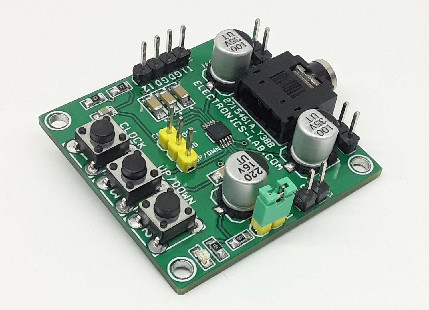
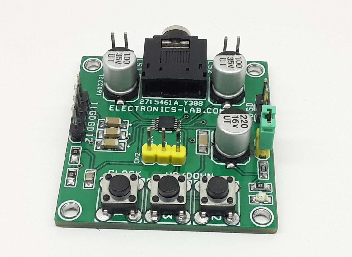
This is a low noise Headphone Amplifier capable of delivering 105mW per channel of continuous average power into a 16Ω load with 0.1% (THD+N) from a 5V power supply. The project is based on the LM4811 chip from the boomer series. The board provides high-quality output power with a minimal number of external components. It features a digital volume control that sets the amplifier’s gain from +12dB to −33dB in 16 discrete steps using a two−wire interface or onboard 3 tactile switches. On-board jumper implements the shutdown feature. The chip also has an internal thermal shutdown protection mechanism.
Connector CN1 Audio Input
Pin 1 Audio Signal Input 1
Pin 2 GND
Pin 3 GND
Pin 4 Audio Signal Input 2
Connector CN3 Power Supply
Pin 1 +5V DC Input
Pin 2 GND
Others
Connector LS1 and LS2: Optional Speaker or Headphone Connection
Connector CN4: 3.5MM Stereo EP Female socket for Headphone
Connector CN2: External/Optional 2 Wire Gain Control
Jumper J1: Closes = Enable, J1 Open Shutdown
LED D1: Power LED
Switch 1: Clock Input, Increment Steps
Switch 2: Volume Down Operation
Switch 3: Volume Up Operation
Features
Operating Power Supply 5V DC
Output 105mW Stereo
On-Board Power LED
Digital Volume Control Range from +12dB to −33dB
“Click and Pop” Suppression Circuitry
THD+N at 1kHz, 105mW Continuous Average Output Power into 16Ω 0.1 % (typ)
THD+N at 1kHz, 70mW Continuous Average Power into 32Ω 0.1 % (typ)
Low Shutdown Current
3 Tactile Switches to set the Gain
Optional 3 Pin Header Connector for 2 Wire Interface for Micro-Controller for Gain
On-Board Stereo EP Socket for Easy Headphone Interface
Optional 2 x Header Connector for Headphone/Speaker Connections
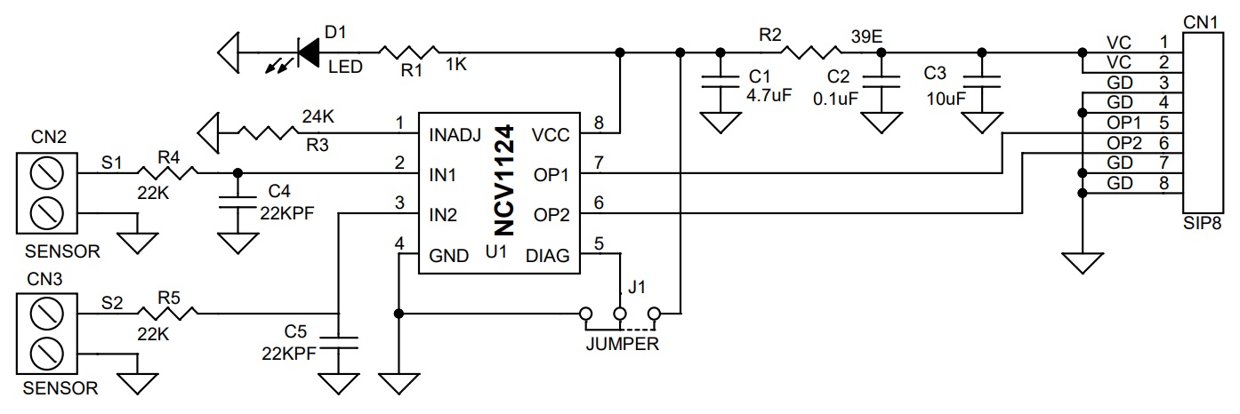
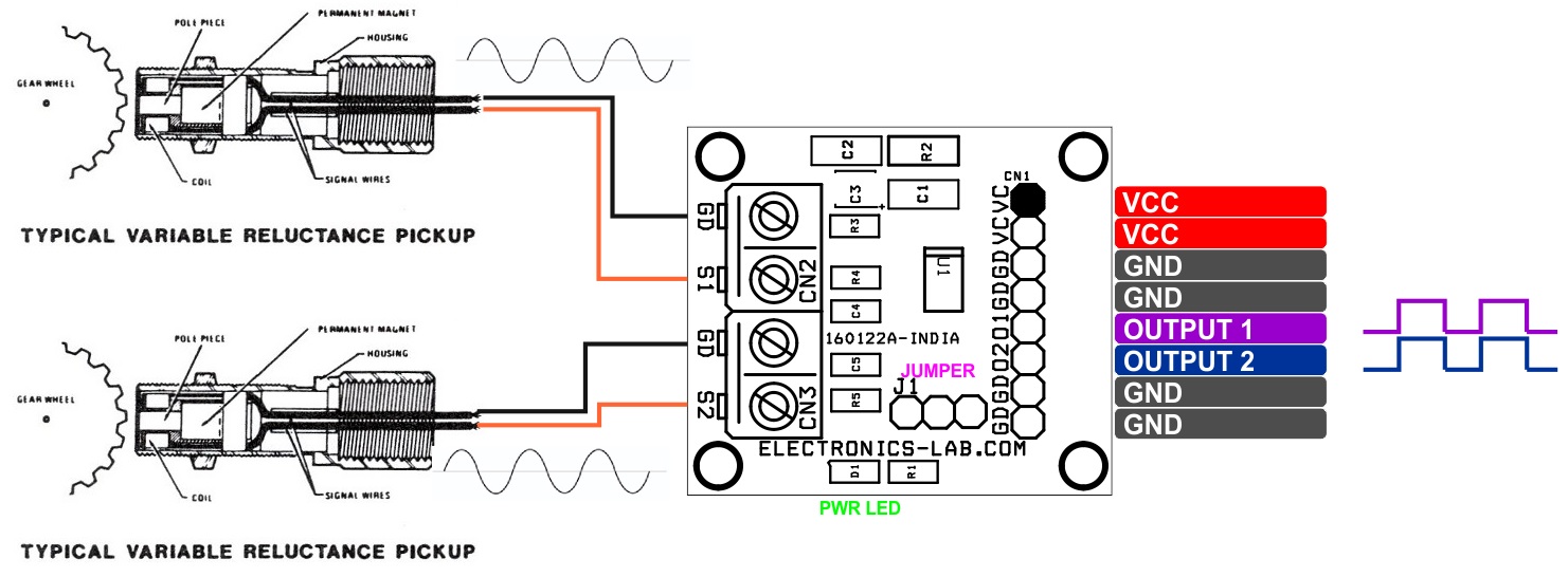
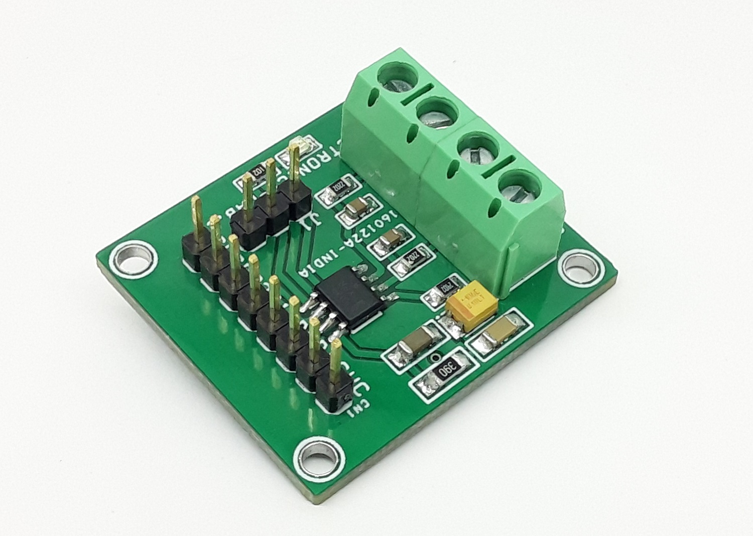
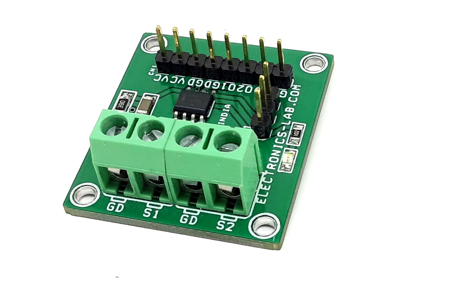
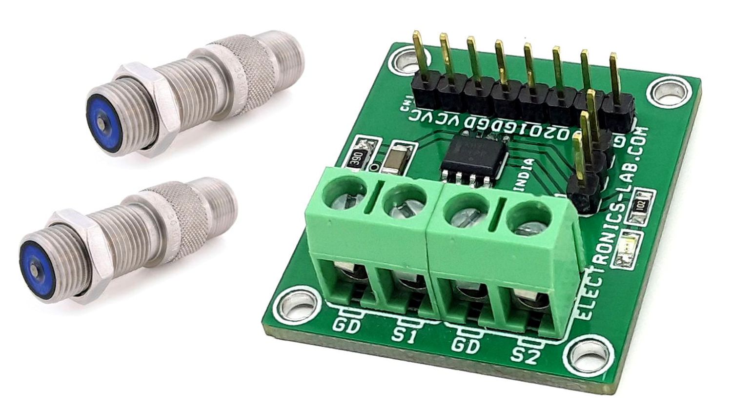
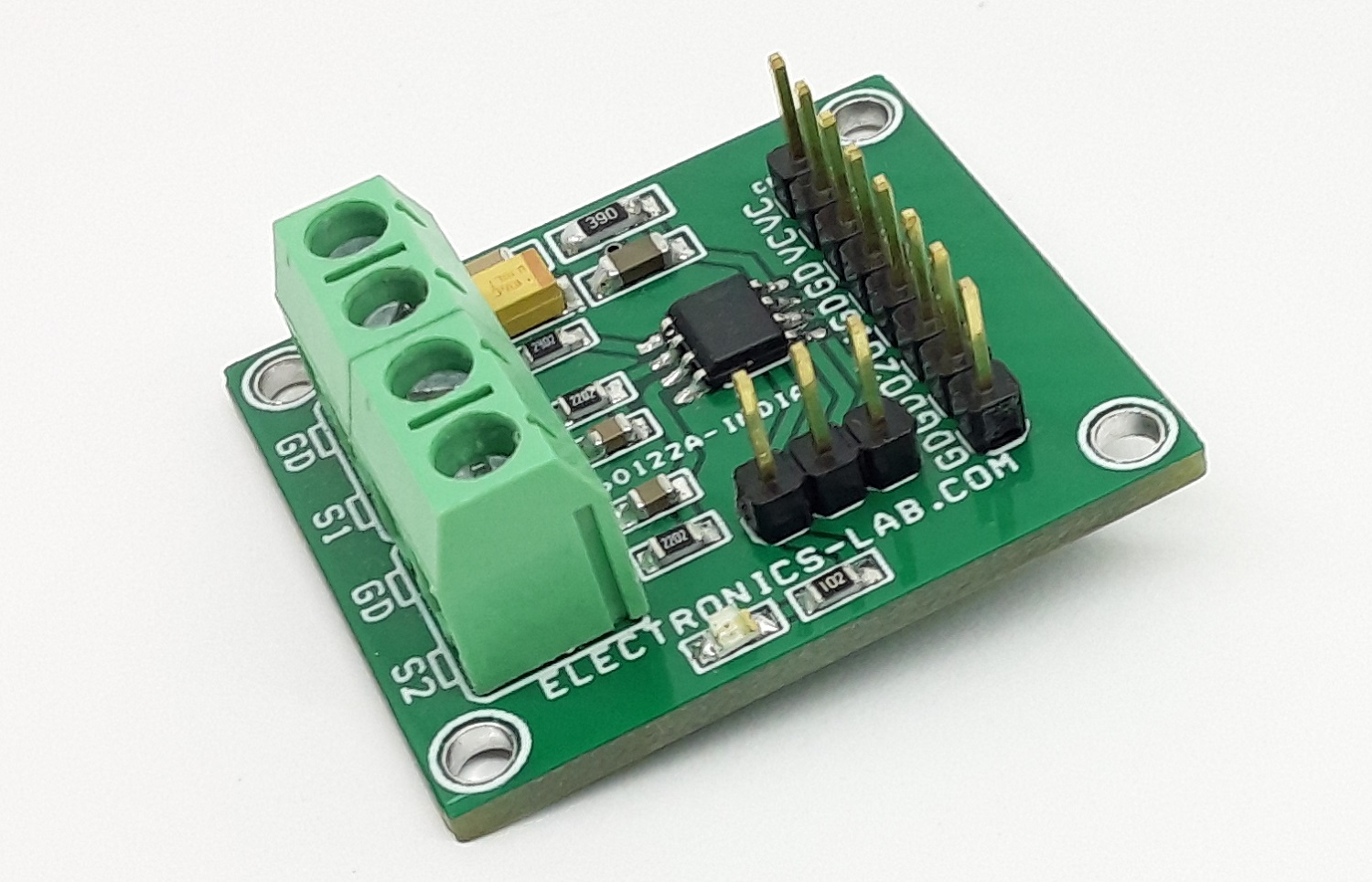
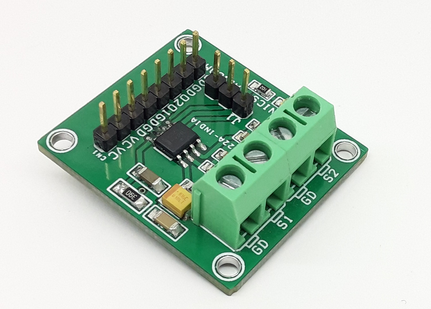
This project offers a dual−channel low component count interface solution for ground-referenced variable reluctance sensors. Each of the two identical channels interfaces with a variable−reluctance sensor, and continuously compares the sensor output signal to a user−programmable internal reference. An alternating input signal of appropriate amplitude at IN1 or IN2 will result in a rectangular waveform at the corresponding OUT1 and OUT2 terminal, suitable for interface to either standard microprocessors or standard logic families. A diagnostic input, common to both channels, provides a means to test for degradation or loss of the physical connector to both sensors. Each channel of the circuit has independent input bias and clamp circuitry, and independent comparators with Hysteresis voltage generators. Both channels share a common reference generator for normal and diagnostic modes. Basically, the circuit converts the sinewave signal of the sensor into a clean rectangular wave signal.
Input Protection
An active clamp is provided on each input to limit the voltage on the input pin and prevent substrate current injection. The clamp is specified to handle ±12 mA. This puts an upper limit on the amplitude of the sensor output. With resistor value R3 = 22 k, then, Therefore, the VRS (pk−pk) IN1 and In2 voltage can be as high as 480 V. The circuit will typically run at a frequency up to 1.8 MHz if the input signal does not activate the positive or negative input clamps. Frequency performance will be lower when the positive or negative clamps are active. A typical performance will be up to a frequency of 680 kHz with the clamps
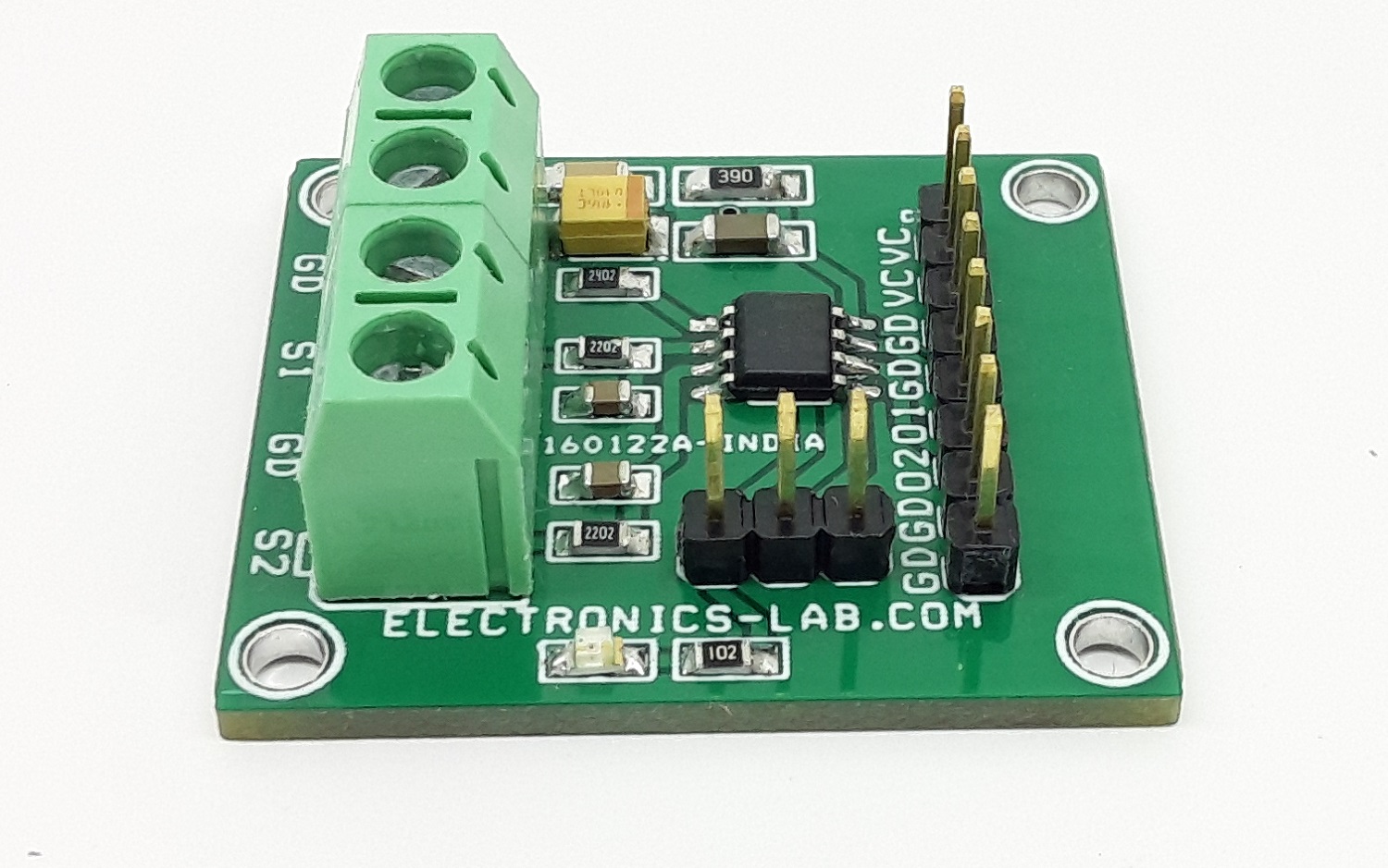
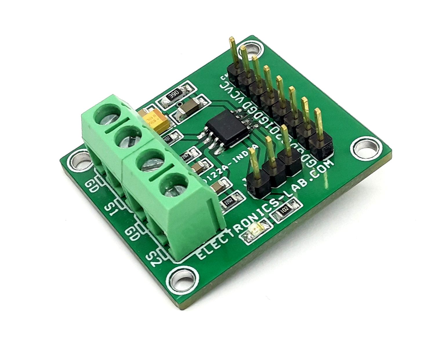
Note: The project is built using an NCV1124 chip, refer to the datasheet of the chip for further information on internal functions.
Connections:
CN2 and CN3 Sensor 1 and Sensor 2 Interface
Jumper 1 Diagnostic Mode Selection
D1 Power LED
CN1: Pin1 and Pin 2 = VCC, Pin 3 and Pin4 = GND, Pin5 = Output 1, Pin6 = Output 2, Pin 7 and Pin 8 = GND
Stepper Motor based 2 Channel Incremental Encoder Channel A and Channel B Phase Shift Output to detect the rotation direction
Other than a reluctance sensor, the project can help to use a stepper motor as a rotary encoder. Connect the 4 wires of a bipolar stepper motor at input terminal S1, GND, and S2 and GND. The project provides 2 channel rotary encoder output channel A and Channel B, the output is 200 Lines per rotation and both outputs are phase-shifted which can help to detect the direction of the encoder.
Applications
Anti−Skid Braking and Traction Control
Vehicle Stability Control
Drive Belt Slippage Detection
Crankshaft/Camshaft Position Sensing
Features
Power Supply 5V DC +/-10%
Two Independent Channels TTL Output
Internal Hysteresis
Input Threshold +/- 160mV
Input Signal Sensitivity 250mV to 250V Peak to Peak
Built−In Diagnostic Mode – Jumper Selection
Site and Control for Automotive Applications
Direct Reluctance Sensor Interface – Screw Terminal Connectors
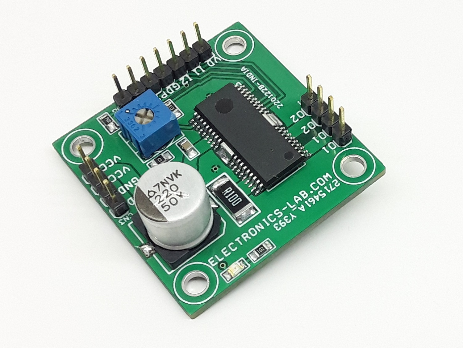
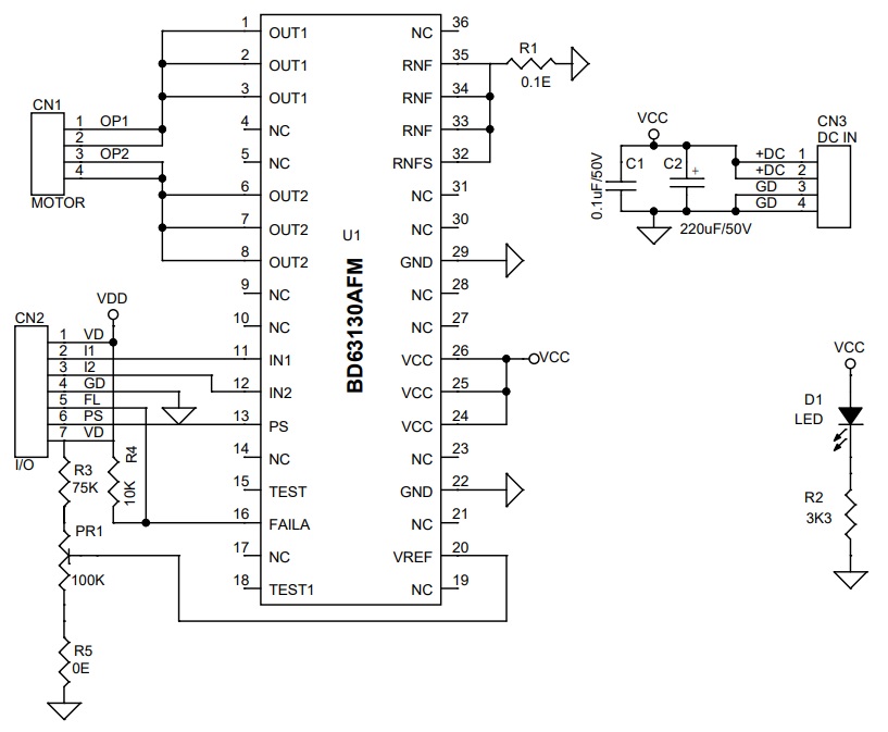
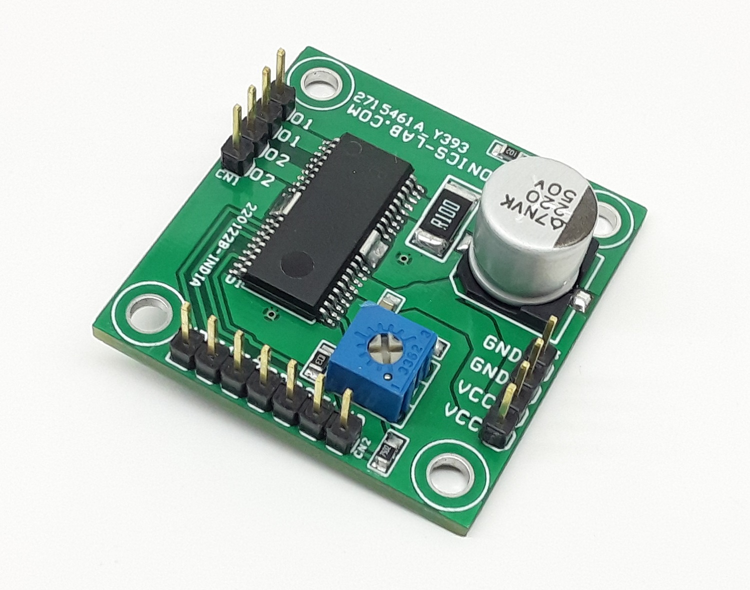
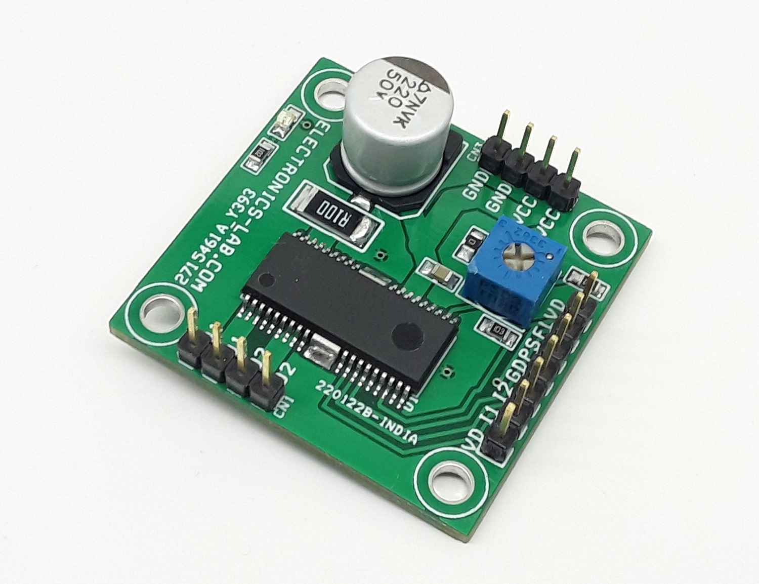
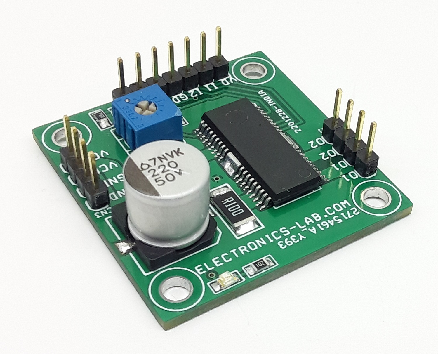
This is a powerful yet small size low profile brushed DC motor drive system with a few key features like adjustable constant current control, direction control, brake controls, Alert output, PWM for speed control etc. BD63130AFM chip is the heart of the project which is an H-bridge motor driver for the DC brush motor. This driver can facilitate low power consumption by direct PWM or PWM constant current control. There are various built-in protection circuits in this IC. It is possible to output an abnormal detection signal for Wired-OR that notifies each protection circuit operation, and this contributes to set high reliability.
Constant Current Mode or Direct PWM Mode Selection
Constant Current Mode: By default, this project works in constant current mode. Constant current can be set using Trimmer Potentiometer PR1. Use Input1 and Input2 of CN2 to control the Motor Forward, Reverse, and Brake, Refer to Table 1 for input logic.
PWM Mode: Replace the resistor R1 with 0 Ohms. Adjust the PR1 trimmer potentiometer to 1 to 2V. Use Input 1 and Input 2 as external PWM/Logic Input, Maximum Allowable PWM frequency 100Khz. Refer to table 4 for input signals.
Features
Single Power Supply Input Range 8 to 46V DC (rated voltage of 50V)
Rated Output Current (peak): 3.0A(4.0A)
Low ON-Resistance DMOS Output
Forward, Reverse, Brake, Open Function
Power Save Function
External PWM Control – PWM Control Mode
PWM Constant Current Control Adjustable (current limit function)
Built-in Spike Noise Cancel Function (external noise filter is unnecessary)
Built-in Logic Input Pull-down Resistor
Cross-conduction Prevention Circuit
Output Detection Signal during Abnormal states (Wired-OR)
Thermal Shutdown Circuit (TSD)
Over-current Protection Circuit (OCP)
Under Voltage Lockout Circuit (UVLO)
Over Voltage Lockout Circuit (OVLO)
Ghost Supply Prevention (protects against malfunction when the power supply is disconnected)
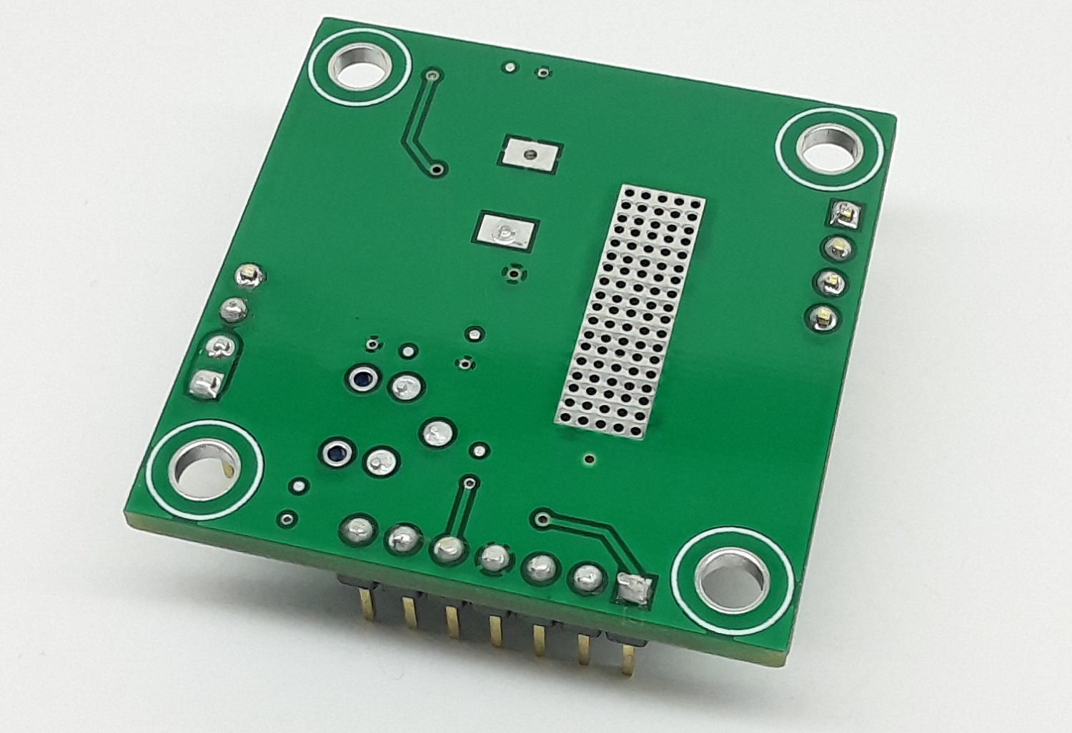
PCB dimensions: 37.47 x 36.83 mm
Inputs and Outputs CN2
Pin1: VDD 5V DC @ 10-20mA- Input
Pin2: Input 1 PWM Input or Logic H/L input Constant for Current Mode
Pin3: Input 1 PWM Input or Logic H/L input Constant for Current Mode
Pin4: GND
Pin5: Fault
Pin5: PS
Pin7: VDD 5V DC @ 10-20mA – Input
CN3 Motor Supply Input
Pin1: +DC 8 to 46V Motor Supply
Pin2: +DC 8 to 46V Motor Supply
Pin3: GND
Pin4: GND
CN4 DC Bushed Motor
Pin1: Motor 1 (Output1)
Pin2: Motor 1 (Output1)
Pin3: Motor 2 (Output2)
Pin4: Motor 2 (Output2)
Trimmer Potentiometer PR1
Constant Current Adjust
LED D1: Power LED
PS/ Power Save Pin Low = Power Same Mode Standby Mode, High=Active
PS can put the circuit into a standby state and make motor outputs OPEN. Be careful because there is a delay of 40μs (Max), as PS=L→H, until it is returned from standby state to normal state and the motor output becomes ACTIVE.
Input1 and Input2 (Refer Table-1)
IN1, IN2/ H Bridge Control Pin It decides the output logic for H-bridge
FAILA/ Fault Signal Output Pin (Refer to Table 2)
FAILA outputs an abnormality detection signal when Over-Current Protection (OCP) or Thermal Shutdown (TSD) operates. Even if Under Voltage Lock Out (UVLO) or Over Voltage Lock Out (OVLO) operates, the FAILA signal doesn’t turn abnormality detection signal (i.e., high). This signal can be connected to the microcomputer and the system can be shut down. This pin is an open-drain type, and a Pull-up resistor R4 is used. Normal output is High, this pin goes low when fault condition arises.
Thermal Shutdown (TSD)
This IC has a built-in Thermal Shutdown circuit for thermal protection. When the IC’s chip temperature rises 175°C (Typ) or more, the motor output becomes OPEN. Also, when the temperature returns to 150°C (Typ) or less, it automatically returns to normal operation. However, even when TSD is in operation if heat is continued to be applied externally, heat overdrive can lead to destruction.
Over-Current Protection (OCP)
This IC has a built-in Over-Current Protection circuit as a provision against destruction when the motor outputs are shorted to each other or VCC-motor output or motor output-GND is shorted. This circuit latches the motor output to an OPEN condition when the regulated current flows for 4μs (Typ). It returns with power reactivation or a reset of the PS pin. The over-current protection circuit aims to prevent the destruction of the IC only from abnormal situations such as when motor output is shorted and it is not meant to be used as protection or security for the device. Therefore, the device should not be designed to make use of the function of this circuit. After OCP operation, if abnormal situations continue and returned by power reactivation or reset of the PS pin happens repeatedly, then OCP operates constantly. The IC may generate heat or otherwise deteriorate. When the L value of the wiring is great due to the wiring being long, if the output pin voltage jumps up and the absolute maximum values may be exceeded after the over current has flowed, there is a possibility of destruction. Also when the current which is the output current rating or more and the OCP detection current or less flow, the IC can heat up to Tjmax=150°C or more and can deteriorate, so the current exceeds the output rating should not be applied.
Under Voltage Lock Out (UVLO)
This IC has a built-in Under Voltage Lock Out function to prevent false operations such as IC output during power supply under-voltage. When the applied voltage to the VCC pin goes 5V (Typ) or less, the motor output is set to OPEN. This switching voltage has a 1V (Typ) hysteresis to prevent false operation by noise etc. Be aware that this protection circuit does not operate during power save mode.
Over Voltage Lock Out (OVLO)
This IC has a built-in Over Voltage Lock Out function to protect the IC output and the motor during power supply over voltage. When the applied voltage to the VCC pin goes 52V (Typ) or more, the motor output is set to OPEN. This switching voltage has a 1V (Typ) hysteresis and a 4μs (Typ) mask time to prevent false operation by noise etc. Although this over voltage locked out circuit is built-in, there is a possibility of destruction if the absolute maximum value for power supply voltage is exceeded. Therefore, the absolute maximum value should not be exceeded. Be aware that this protection circuit does not operate during power save mode.
Ghost Supply Prevention (protects against malfunction when the power supply is disconnected) If a control signal (IN1, IN2, PS, and VREF) is applied when there is no power supplied to the IC, there is a function that prevents a malfunction where voltage is supplied to the power supply of this IC or other IC in the set via the electrostatic destruction prevention diode from these input pins to the VCC. Therefore, there is no malfunction in the circuit even when voltage is supplied to these input pins while there is no power supply.
PWM Constant Current Control(Table 3)
This function can limit the peak current such as switching current in driving the DC brush motor.
Current Control Operation: The output current increases due to the output transistor being turned on. When the voltage on the RNF pin, the output current is converted it due to connecting the external resistance to the RNF pin, reaches the voltage value set by the VREF input voltage, the current limit comparator engages and enters current decay mode. Thereafter the output turned on again after a period of time determined by the CR pin. The process repeats itself constantly.
Blank Time (Fixed in Internal Circuit): In order to avoid misdetection of the current detection comparator due to RNF spikes that occur when the output turns ON, the internal voltage between 0.4V and 0.8V is provided as minimum ON time (tONMIN 1.5µs Typ). During this time, the current detection is disabled after the output transistor is turned on. This allows for a constant-current drive without the need for an external filter.
Internal Timer (Fixed in Internal Circuit): Repeat charging and discharging between 0.4V to 0.9V internal voltage determined by IC internal circuit. When internal voltage is changed charge from discharge, the output is then ON from the current decay mode.
The global semiconductor giant STMicroelectronics has simplified interaction with trained devices with its new inertial sensor ISM330ISN featuring an Intelligent Sensor Processing Unit (ISPU). ISPU is essentially a low-power, high-performance programmable core with high computational efficiency. As a result, this processor will be able to execute the signal processing and AI algorithms in real-time. Before transmitting data to the MCU and gateway/cloud, the ISPU processes data without waking up the system. In addition to 32KB of program memory and 8KB of data memory, ISPU has an FPU capable of performing addition, subtraction, and multiplication. This special processor enhances machine-learning applications and reduces power consumption and also its size by up to 50% making it superior to other typical MCUs.
The ISM330ISN has an “always-on” 6-axis Inertial Measurement Unit (IMU) for detecting precise motion and position. The IMU provides incomparable accuracy and performance for its compact size by using the intelligence embedded in this sensor. ISM330ISN’s embedded intelligence allows it to perform advanced motion detection functions without interacting with an external MCU. Thus, helping in consuming less power at the system level.
ISM330ISN’s Features
The ISM330ISN supports programmable interrupts as well as an on-chip sensor hub with up to six sensors. The six sensors include two internal sensors, a 3-axis accelerometer and the 3-axis gyroscope and four other external sensors.
The selectable full scale for the accelerometer and the gyroscope is ±2/±4/±8/±16 g and ±125/±250/±500/±1000/±2000 DPS respectively.
With sensor hub functionality, it is possible to collect data from up to four external sensors.
The sensor guarantees consistent high accuracy with the ISPU while utilizing merely 0.59mA in combination mode with the accelerometer and gyroscope engaged.
ISM330ISN provides up to 70 μg/√Hz low noise sensing in high performance and the output data rate of 6.6Hz
This inertial sensor gets the support of SPI / I2C serial interface protocols.
The developers can use NanoEdge AI Studio to program the ISPU. It is a market-proven ST product and also a developer’s choice to build AI applications on STM32 microcontrollers. With this tool, anybody can simply construct strong machine learning libraries that use on-sensor learning.
ISM330ISN’s Pin Diagram
The ISM330ISN is a 14-pin sensor that has the same dimensions of 3mm x 2.5mm x 0.83mm as other conventional inertial sensors. While interfacing with the host, ISM330IS provides two modes of operation and functionality.
Mode 1: I2C or SPI (3- and 4-wire) serial interface is available.
Mode 2: I2C or SPI (3- and 4-wire) serial interface and I2C interface master for connecting external sensors are available.
The following table describes the functionality of each pin in mode 1 as well as mode 2 respectively.
See the user manual for more information about ISM330ISN’s pin diagram and features.
During an event, Simone Ferri, General Manager of Marketing, Analog MEMS and Sensors Group, STMicroelectronics said “Intelligence which was once implemented at the network edge, in an application processor, is now being implemented at the deep edge, inside the sensor”. Mr Ferri continued “Our ISM330ISN IMU ushers in a new generation of smart sensors, employing integrated AI to handle complex functions like pattern recognition and anomaly detection with much higher efficiency and performance.”
Coming from ST’s iNEMO family of IMUs, ISM330ISN is ideal for IoT purposes. It has applications in industrial robotics, asset tracking, anomaly detection and condition monitoring. This smart sensor can be equipped with alarms for event detection or even in smart homes. It is also beneficial in complex motion sensing and gesture recognition for personal health
ST’s 10-year longevity program protects the ISM330ISN, which provides a guarantee to the product designers and manufacturers of long-term product availability. The ISM330ISN is set to go into production in H2 2022 and will cost $3.48 for purchases of 1000 pcs. For more updates about this product visit ST’s official website.
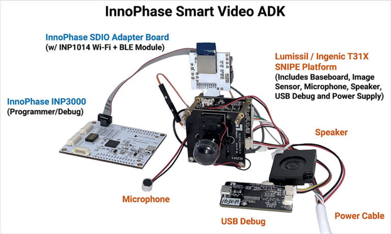
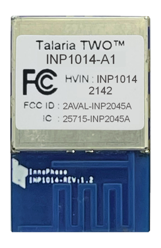
Specialist in extreme low-power wireless IoT modules and a fabless semiconductor company, InnoPhase has announced its partnership with Ingenic Semiconductor Co Ltd. which is known to be superior in the world of microprocessors and CPU technologies. The primary aim of this partnership is to jointly market AI-vision systems. This remarkable collaboration has launched its Smart Video ADK (Application Development Kit) based on InnoPhase’s Talaria TWO WiFi module and Ingenic’s T31 Video Processor.
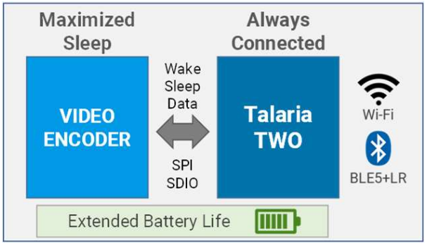
The incredible run of this Smart Video ADK is largely due to Talaria TWO and T31 video processors. Talaria TWO Wifi Module‘s digital radio offers ultra-low power cloud connectivity and T31 Video Processor provides quick, high-performance image processing. Providing deep learning algorithms, Smart Video ADK enables a user to create cutting-edge solutions. Integrating the Smart Video ADK with high-performance video processing and Wi-Fi networking made it possible to build a low-power device.
Specifications of Core Components
The SoC’s novel architecture meets the requirements of video devices such as high-performance processing and encoding of high-quality photos and videos.
The CPU provides ultra high-frequency up to 1.5GHz and an independent RISC-V lite core. This video processor also gets an SMD128-based Vector Deep Learning accelerator enhancing the 3D graphics and audio/video processing.
It consists of an H.264/H.265/MJPEG video encoder having a maximum resolution of 2592 x 1920 at 30fps along with a memory capacity of 512Mbit or 1Gbit.
Ingenic’s T31 video processor includes low light and surveillance scenario-specific optimizations. It features 2D / 3D noise reduction and distortion correction to achieve clear image quality for better object recognition.
The featuring integrated Audio Codec encodes/decodes the echo-less audio with the support of an I2S interface for the video processor.
The T31 video processor has applications such as mobile cameras, security surveys, video analysis, and video and voice communication.
For more information on this video processor, visit the official website.
InnoPhase Talaria TWO Wifi Module
The Talaria TWO platform is the most power-efficient solution with single-band 802.11b/g/n Wi-Fi and Bluetooth Low Energy (BLE) 5.0 long-range wireless standards.
With the Arm Cortex-M3 running at 800 MHz, it supports maximum frequency up to 2.4GHz.
The Talaria TWO consists of an SDIO peripheral interface to link with the T31 video processor.
Ultra-low-power Wi-Fi maintains internet/cloud connectivity for battery-based products. It also features a “Dual-Stack” software that divides the processing work between the T31 and Talaria TWO for low power consumption.
Due to its exceptionally low constant current, the device facilitates a new generation of battery-operated direct-to-cloud IoT devices.
Smart homes and surveillance, asset tracking, smart buildings, and equipment maintenance can be some of its applications.
For more information on InnoPhase Talaria TWO check out our blog.
Smart Video ADK’s modes of operation
A user can operate this smart video kit in two modes:-
Wi-Fi Idle Connected Mode
Talaria TWO is linked to a Wi-Fi router, where it processes beacons and sends Keep-Alive messages as needed.
Ingenic T31 Video Processor platform is completely shut down
Active Video Capture Mode
The Ingenic T31 actively captures video in High-Resolution/30fps and transmits it to the Talaria TWO through the SDIO interface.
Talaria TWO remotely transmits vast data packets utilising high-bandwidth Wi-Fi.
Smart Video ADK’s Long Lasting Battery Life
The main focus of this Smart Video ADK is to provide a less power-consuming battery. As a result, the idle Wifi usage is incredibly low, allowing the active video capturing mode to use its maximum power. The estimated battery life is 14.4 months on a 3000mAh while operating at a 99.3% idle with a 0.7% video capture ratio. This will give rise to AI cameras that can work for several months on a single charge under any circumstances.
Standard Linux commands can easily control and instruct the Wifi and BLE wireless connections. The Ingenic T31 provides Linux drivers as well as AI algorithms for person detection, facial detection/recognition, cry detection, vehicle detection, pet detection and also quick start and user guides. Therefore this Smart Video ADK can be used as security cameras, baby monitors, access control systems, and identity verification systems.
In the press release Wiren Perera, Vice President and the General Manager at InnoPhase said
“The incredible power efficiency of InnoPhase’s wireless modules along with Ingenic’s industry-leading T31 video processor will be a game-changer for our joint customer.”
To know more about the product and its availability, visit the product page.
Since machine vision is increasingly becoming important in the field of robotics development, several top-level companies in the robotic industry are taking interest in projects that aid the rapid development of hardware-accelerated applications for robotics, machine vision, and communication and control.
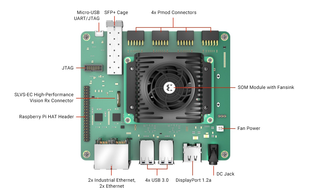
AMD-Xilinx recently designed the Kria KR260 Robotics Starter kit for robotics and industrial applications, complete with the high-performance interface, a standard framework, and native ROS 2 support. The AMD-Xilinx Kria KR260 is indeed a robotic starter kit for the future. It is the latest addition to the Kria portfolio of adaptive SoMs and developer kits, offering a seamless path to production deployment with existing Kria K26 adaptive SoMs.
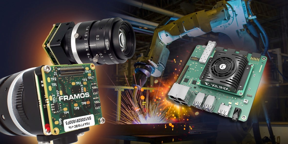
On the other hand, Framos, a certified partner of AMD-Xilinx, and one of the leading companies in the supply of custom vision solutions and imaging components has also now introduced a new fully integrated camera accessory for the Robotics Starter kit.
The newly launched FSM-IMX547 camera accessory is capable of streaming high-quality monochrome or color images to the Robotic starter kit. It is compatible with the 10GigE Vision camera app available for free download and testing purposes at the AMD-Xilinx App store. The camera kit is equipped with a 5 MegaPixel shutter CMOS image sensor which it uses to transmit color or black/white images to the starter kit at up to 12fps. It also uses Framos’ SLVS-EC Rx IP, allowing the starter kit to stream at up to 2472 x 2128 pixels effortlessly. According to Nathan Dinning, the Director of Product Management at FRAMOS,
“the most demanding imaging projects in the robotics industry that require robust data transfer will leverage this technology to its full extent. The SLVS-EC high speed interface paired with the Kria KR260 is a powerful combination that will give Vision to a new age of robotics.”
The camera modules offer input voltages of 1.1V, 1.8V, 2.9V, and 3.3V. They are designed specifically for applications that require mid-to-high resolution with a fully-featured sensor. The FSM-IMX547 camera modules and its versatile adapter framework is also a camera kit for all levels of product creation, especially at the evaluation and proof-of-concept stages where they can be used to interface the Kria KR260 Robotics Starter Kit or other open processing platforms with the latest image sensor technology.
Other specifications include 2.74µm pixel pitch, 1/1.8 type optical format, 5:4 aspect ratio, and I2C communication interface. The kit can also be used to develop machine vision applications with high-speed, high-performance, and high output. Included in the package as accessories are a matching lens and a corresponding amount to give the best out-of-the-box experience to users.
Other useful information and availability of the Kria KR260 Robotics Starter Kit can be found on the company’s product page, while product details of the monochrome version of the FSM-IMX547 camera accessory are available on Mouser’s website here, and the color version can be found here.
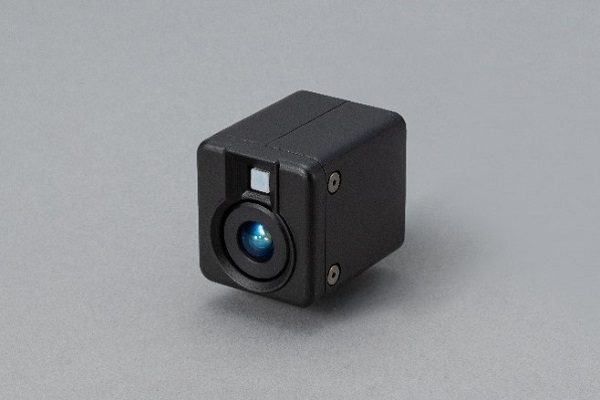
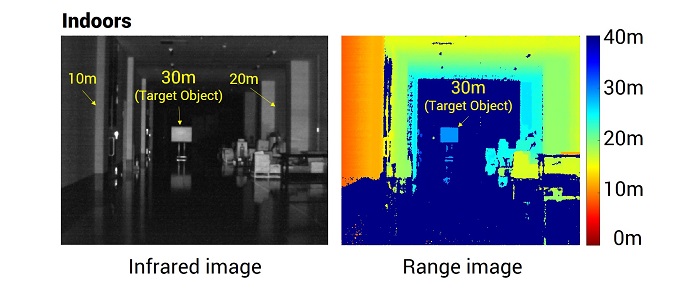
Japanese communications and embedded device manufacturer, Brookman Technology, collaborated on using a hybrid Time-of-Flight method developed by Prof. Shoji Kawahito of Shizuoka University. The collaboration has led to the (as claimed) “world’s first” next-generation 3D Time-of-Flight (ToF) distance sensor, which is capable of operating over a distance of up to 30 meters. This sensor is able to measure an expanded range which is more than 5x that of a traditional indirect ToF-based 3D sensor.
Brookman Technology’s ToF 3D range sensor uses CMOS image sensor capabilities to provide enhanced image quality for autonomous drones and robot carriers. The hybrid ToF 3D sensor also has a light canceling function, which also makes it the “world’s first” CMOS image sensor that can measure a distance of up to 20 meters under illuminance of 100,000 lux.
“Together with Brookman Technology, we hope these new sensors will contribute to greater safety and convenience by functioning as ‘3D sensing eyes’ that expand the possibilities for autonomous robots and industrial devices,” said Tatsuo Noguchi, head of Toppan’s ToF Business Development Center. “Toppan will drive further development of cameras with range sensors employing the new ToF technology.”
The key features of the new ToF sensors are the measurement distance, noise cancellation function, high-speed imaging, and simultaneous operations. As mentioned earlier, the use of a hybrid ToF method makes the new 3D sensor capable of working at a measuring distance of up to 30 meters. For high-speed imaging, the ToF sensor does not blur the image to cause errors but also eliminates ambient light noise in a single frame. The sensor can take a maximum of 120 range images per second, which is approximately four times that of the existing techniques. The simultaneous operations also provide a unique control to cancel out signals emitted from other cameras, making it possible to work with up to 256 cameras without the interference of signals.
Further details on the ToF sensor technology have been presented by Toppan, Brookman Technology, and Shizuoka University at the 2022 IEEE Symposium on VLSI Technology & Circuits (VLSI Symposium). According to the company, testing and validation of the sensors will begin in December 2022 with commercial sales in Fall 2023.