TI unveils new buck converters and LDO linear regulator at APEC

TI introduced two new buck converters and an LDO linear regulator at APEC 2022 that address design challenges for automotive and industrial systems.

Texas Instruments (TI) will launch three new power ICs and address power-management design challenges for electric vehicles (EVs) and industrial systems at the Applied Power Electronics Conference (APEC) 2022. The new products include the LMQ66430 and LMQ66430-Q1 buck converters and TPS7A94 low-dropout (LDO) linear regulator.

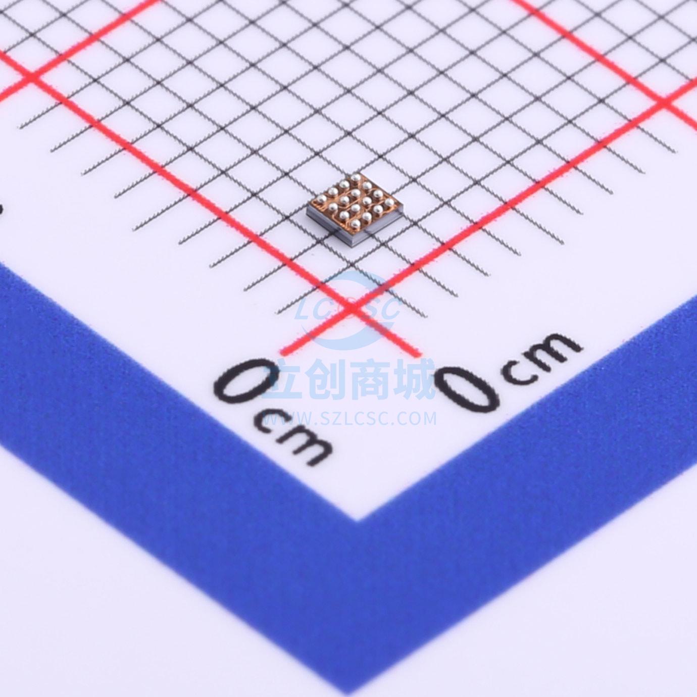
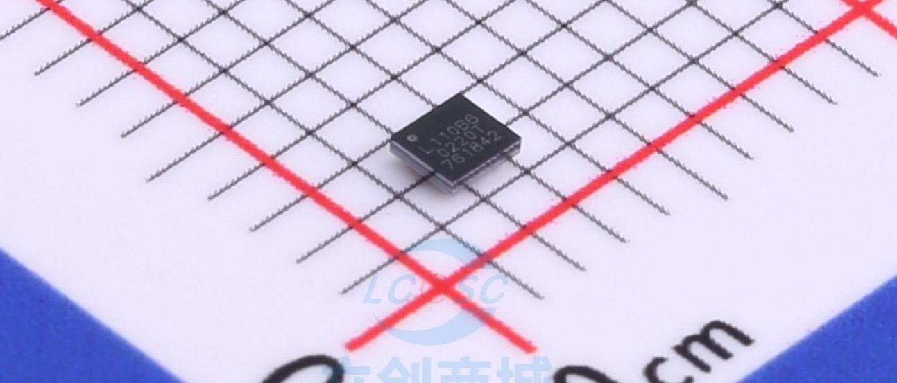
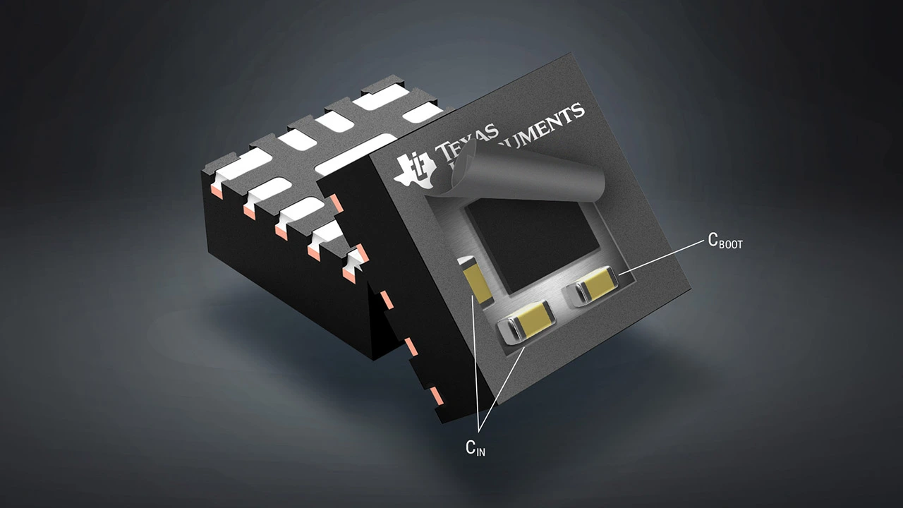
The new 36-V, 3-A LMQ66430 and LMQ66430-Q1 buck converters are designed to lower electromagnetic inductance (EMI) in automotive and industrial applications while improving filter size. The devices integrate two input bypass capacitors and one boot capacitor. This enables engineers to meet Comité International Spécial des Perturbations Radioélectriques (CISPR) 25 Class 5 EMI standards while claiming a best-in-class total solution size of of 114 mm2, 1.5-µA quiescent current (IQ), and reduced bill-of-materials costs.

By integrating the three capacitors in a 2.6 × 2.6-mm enhanced QFN package, it allows for a super small solution, and the benefit to customers is a much smaller EMI passive filter, said Carsten Oppitz, vice president and general manager, buck switching regulators  at TI.

“By integrating the bypass capacitors very close to the die, we are reducing the internal inductance, which means we have very little overshoot in the switching,” he said. “This eliminates the interference where it’s usually produced. This means we don’t have to filter so much compared to a standard solution where there is a big passive filter that leads to increased weight of the system and increased size of the system.”

Designed to enhance the power and signal integrity of low-voltage devices thanks to its low noise, the TPS7A94 LDO linear regulator claims the industry’s lowest noise of 0.46 µVRMS – at least 42% better than competing solutions – with a high power-supply rejection ratio (PSRR). This helps designers improve system accuracy and precision in highly sensitive applications.

“Low noise is especially critical in certain types of high-precision analog systems. This includes test and measurement, medical, and telecom applications that really require a very clean power rail,” said Alex Chin, vice president and general manager, linear power at TI.

“Even a small amount of noise can have a negative effect on the performance of noise-sensitive circuits. So, for example, think about server and telecom applications, they’re evolving to accommodate more users and to keep up with more demand for precise signals and even higher date capacity,” said Chin. “Without super-low-noise power rails, the next generation of communication systems will fail to increase the channel density and even the data rates needed to accommodate the increase in both the number of connected devices and the data that each consumes.”

One of TI’s newest devices, the TPS7A94, offers the lowest noise for high precision and high accuracy applications, he said. “With the TPS7A94 we’re adjusting two main noise sources of a power rail. The first one is driving the inherent noise generated by the LDO down to industry leading levels, while also providing amazing PSRR performance to clean up the noise coming from the upstream power supply.”

“The inherent noise from the TPS7A94 LDO is at the industry’s best at 0.46 µVRMS from 10 Hz to 100 kHz and we’re at least 42% better than competing solutions,” said Chin. “Secondly, we’ve also provided 100 dB of PSRR at 1 kHz, while also achieving more than 60 dB at 1 MHz to filter out the upstream power supply. We do this while also providing the solution with a very low dropout making it the most efficient LDO with a typical dropout of 150 mV at 1 A.

Chin also noted the TPS7A94 does not require additional filtering components, which makes the design smaller and more cost-efficient.

4th Generation Ultra Low Power Temperature Sensor for Battery-Driven Designs

Sensirion has launched its fourth-generation series STS4x which features low power consumption and is well-suited for mass production and battery-driven designs. The digital I2C interface of this series enables operation without external signal disturbance, while proven production processes guarantee the highest reliability in the field. Moreover, with its tiny footprint of only 1.5 × 1.5 × 0.5 mm3, the dual-flat no-leads (DFN) package can easily be integrated into various applications.

With functionalities like enhanced signal processing, three distinctive I2C addresses, and communication speeds of up to 1 MHz, all sensors in this series offer top performance. It features a wide supply voltage range of 1.08 to 3.6 V and low current consumption of 0.4 µA for a typical average current measured once per second that allows the series to be implemented into battery-driven designs.

Key Features

  • Temperature accuracy: up to ±0.2°C
  • Supply voltage: 1.08 V … 3.6 V
  • Average current: 0.4 µA (at meas. rate 1 Hz)
  • Idle current: 80 nA
  • I2C fast mode plus, CRC checksum
  • Available with multiple I2C addresses
  • Operating range: -40…125°C
  • NIST traceability
  • JEDEC JESD47 qualification
  • Mature technology from global market leader

more information: https://sensirion.com/products/catalog/STS40-DIS/

Foundries.io and Arduino presents Pro Portenta X8 for Secure IoT Solutions

Foundries.io and Arduino announce their partnership to deliver secure, cloud-based embedded Linux IoT and Edge solutions for enterprise with the flagship Arduino Pro Portenta X8 system on module (SoM). Arduino Pro Portenta X8 is an SoM that combines a Linux-based PaaS with docker support to the functionality of a Portenta H7 SoM.

Security factor determines the scalability of the target application for IoT or Edge products, thus an agile infrastructure plays a significant role in making the solution fitter for the industry.

This product enables secure management and maintenance of IoT devices because all the software needed to securely update edge devices is provided through a robust DevOps platform. The IoT and Edge devices market is expected to grow in the next five years. It’s the responsibility of every Linux-based device maker to handle security, testing, and maintenance, but for many this requires they branch out into a completely different field of networking and security.

The solutions for enterprise businesses must handle cyber security of these devices and dedicated infrastructure for maintaining the Linux OS., firmware, and applications. Foundries.io solves these issues through a utility called FoundriesFactory, a cloud-based DevOps service to build, test, deploy, and maintain IoT and edge devices. It accelerates product firmware, OS, and applications development, and provides support for monitoring and incremental Over The Air (OTA) updates of the Linux OS, firmware, and applications of devices and fleets.

Hence, Arduino and Foundries.io, each with their respective expertise, simplified the approach for a ready-to-use solution that can help our customers build IoT and edge systems with confidence. By embedding a FoundriesFactory in the Arduino platform, customers can be sure to choose the best solution on the market.

Portenta X8 top
Arduino Pro Portenta X8

Previously, Arduino pioneered a new product category by integrating microcontrollers and microprocessors on a single hardware platform. Now Arduino Pro Portenta X8 aims to take this experience to the next level by providing the same flexibility to enterprises.

The combination of the Portenta X8 and the FoundriesFactory basically provides a robust microcontroller for IoT edge devices with infrastructure to maintain and secure the underlying Linux OS. Besides, cloud support gives freedom of choice for connectivity to public or private cloud services. Plus, docker container support and orchestration can maintain a whole fleet of edge and IoT devices through FoundriesFactory.

FoundriesFactory is accessible for the Pro Portenta X8 hardware platform. Users can immediately connect Arduino Portenta X8-based products to the cloud and start developing container-based applications through in-built docker support, leveraging device management and DevOps capabilities. Some of the support features provided by FoundriesFactory concerning software development, device management, and OTA maintenance are:

FoundriesFactory Software Support

foundries-tech-stack

The FoundriesFactory service provides many open source projects as a service combined to form a complete software platform. Since individual components are open source, they can be easily customized as per product requirements and add your proprietary IP.

FoundriesFactory implements software engineering concepts of CI (continuous integration) for testing and maintenance of edge devices. The user can store privately source code for different builds using git management. The CI pipeline gets triggered for each commit to building the latest code. It also allows testing on local or remote devices without re-flashing.

Once development is completed, it is easy enough to promote to release through the above CI pipeline. This could enable the user to deploy updates as needed based on the use case, compliance and market requirements.

Apart from this, it has full support for Docker containers (optional) to simplify the orchestration of edge devices and services. Also, the user can customize some of the OS code as per the hardware and application use case.

FoundriesFactory Device/Fleet Management

The user can provision secure devices with individual keys during or post-manufacture to leverage external Hardware Security Modules for secure protocols.

Also, the user can update remote devices and fleets using the Factory CLI or REST API and get secure access to remote devices through a VPN service.

To know more about FoundriesFactory services, please visit this link.

FoundriesFactory – OTA Update Feature ArchitectureOTA Architecture

Edge devices communicate with the device gateway using mutual TLS. The device gateway provides a set of REST APIs to support aktualizr-lite, fioconfig and docker authentication.

Aktualizr-lite and fioconfig run as separate daemons that periodically poll the device gateway with HTTP GET requests on configurable intervals. Due to the fact devices are polling the server, REST API changes requested by fioctl happen asynchronously.

Aktualizr-lite validates available targets that a device may install. The algorithm followed for OTA updates on edge devices is:

  1. Check for new root.json. This allows a device to know about key rotations before going further.
  2. Request for timestamp.json metadata.
  3. Request for the snapshot.json metadata.
  4. Ask for the targets.json metadata.

At this point, the device will have all the details regarding new updates and install the latest target build accordingly.

This explains all about Arduino Pro Portenta X8 and FoundriesFactory integration to deliver enterprise-ready cloud-based Linux solutions to secure and maintain hardware OS.

Doogee S98 Set To Launch On March 28th With A Fresh New Look And A Maasive Discount

The new S98 rugged phone was announced last week by Doogee. The company will launch the rugged phone next month on AliExpress and Doogemall (the company’s official shopping platform).

To recap the features of the Doogee S98. Firstly, it comes with a round rear display. The second display looks like a smartwatch completed with stylish bezels. The display also allows a great level of customization by users. Uses include controlling music, checking the time, battery level, and keeping up with notifications among others.

Also on the back of the phone is a Triple camera setup, the main 64MP main, an 8MP wide-angle camera, and the most interesting of the set, a 20MP night vision camera. The night vision camera allows you to capture and record videos in pitch-black environments. Thanks to the infrared light on the side, a clear picture is almost always guaranteed.

Under the hood, MediaTek helio G96 runs the show. The octa-core processor is designed for gaming which means faster performance.

Doogee S98 – | Gaming performance test | Antutu benchmark score |

The battery on this beast is a 6000mAh battery capable of carrying you 2-3 days of active use depending on your usage behavior. It comes with a 33W fast charger and supports a 15W wireless charger.

The main screen is a 6.3” FHD+ corning gorilla glass-protected display. It will run Android 12 out of the box which brings a host of advantages on the security and optimization front. It also comes with a fingerprint scanner and a custom button on either side of the phone. The features are completed with NFC, 4 navigational satellite support, toolkit, custom button, side mounted fingerprint scanner and many more

Not to forget, S98 is waterproof, drop-proof, and can withstand extreme weather.

Doogee S98’s global launch has been booked for March 28. Between March 28th and April 1st, it will be at its lowest price. We will keep you updated when Doogee reveals the price. But, if you want a free S98, Doogee is giving away 8 of them. To throw your hat in the ring, check the official S98 page for more details on the giveaway.

Win a Digilent Analog Discovery Pro 3000 ADP3450

Enter for free…

This month oemsecrets.com has partnered with Digilent to give away an Analog Discovery Pro ADP3450 worth $1295. To enter simply follow the link below for your chance to win.

Get additional entries into the giveaway by sharing this link on Instagram, LinkedIn, Facebook or Twitter using #oemsecrets or @oemsecrets or by following us on LinkedIn.
ENTER FOR FREE

About the Analog Discovery Pro ADP3450

The ADP3450 is the first in the line of Analog Discovery Pro devices and take the analog and digital instruments from the internationally popular Analog Discovery and turn up key functionalities to meet the growing need for professional-level home electronics test benches…read more

Terms and Conditions

This competition is managed and hosted by OEMSECRETS LIMITED, where the precondition for competition entry, for a chance to win an Analog Discovery Pro 3000 ADP3450  is an email subscription to the oemsecrets.com mailing list. This includes the latest electronics industry updates, offers, and product news from OEMSECRETS LIMITED. Subscribers can change preferences or unsubscribe at any time using the links in the footer of any email sent to you from OEMSECRETS LIMITED. The competition closes on 29th April 2022 at 11.59 BST. The winners will be announced the following week via email and on social media. We will contact the winners by email and request shipping information to send the product via UPS tracked shipment and paid for by us worldwide. If we do not hear back via email after two attempts of making contact within 14 days, the prize will be forfeited and a new winner will be chosen.

Audio Line Receiver using INA134

The project described here is a differential line receiver consisting of high-performance INA134 OPAMPs with on-chip precision resistors. The project is fully specified for high-performance audio applications and has excellent AC specifications, including low distortion (0.0005% at 1kHz) and high slew rate (14V/µs), assuring good dynamic response. In addition, wide output voltage swing and high output drive capability allow use in a wide variety of demanding applications. The INA134 on-chip resistors are laser trimmed for accurate gain and optimum common-mode rejection. Furthermore, excellent TCR tracking of the resistors maintains gain accuracy and common-mode rejection over temperature. Operating power supply ±4V to ±18V (8V to 36V total supply).

Audio Line Receiver using INA134 – [Link]

Audio Line Driver using DRV135 with Balanced Output

The project presented here is a differential output amplifier that converts a single-ended audio signal input to a balanced output pair. This balanced audio project consists of high-performance OPAMPS with on-chip precision resistors. They are fully specified for high-performance audio applications and have excellent AC specifications, including low distortion (0.0005% at 1 kHz) and high slew rate (15 V/µs). The board is based on DRV135 from Texas Instruments.

Audio Line Driver using DRV135 with Balanced Output – [Link]

SparkFun Join Hands With MikroElektronika to design new electronic embedded products

MIKROE x SparkFun Partnership

Serbian electronics embedded manufacturer MikroElektronika is known for releasing one product every day, has now been selected by SparkFun under a new partnership agreement to add new products from the MIKRO ecosystem to the SparkFun e-store. The collaboration will also see fresh products being developed, starting with two new SparkFun Originals with mikroBUS sockets that can interact with Qwiic connect system and MicroMod. SparkFun MicroMod mikroBUS carrier board leverages the onboard Raspberry Pi’s in-house silicon tapeout RP2040 microcontroller and is designed for the Feather board form factor, including a microSD card slot and a JST single-cell battery connector. The other product is a SparkFun MicroMod mikroBUS carrier board with a MicroMod M.2 socket and microBUS 8-pin header that provides a greater degree of freedom to interface with any processor board in the MicroMod ecosystem as well as any Click board in the microBUS ecosystem.

Coming back to the key highlight of SparkFun RP2040 mikroBUS development board priced at $14.95 is integrated with 16MB of flash memory and a programmable WS2812 RGB LED. The onboard RP2040 microcontroller features two Arm Cortex-M0+ processors clocked up to a frequency of 133MHz and incorporates 264kB of embedded SRAM in six banks, 6x dedicated IOs for SPI flash memory, 30x multifunctional GPIOs for dedicated hardware, programmable IOs, and 4x 12-bit ADC channels. However, the Feather form factor board only gets 18x multifunctional GPIO pins divided as up to 2x UART, I2C and SPI buses, up to 8x 2-channel PWM and 4x 12-bit ADC channels with an internal temperature sensor (500kSa/s). On the software side, the RP2040 microcontroller supports both C/C++ and MicroPython cross-platform development environments including easy access to runtime debugging.

SparkFun RP2040 mikroBUS Development Board

To power the SparkFun RP2040 mikroBUS development board, the board is designed with a USB Type-C connector and supports a 2-pin JST connector for a LiPo battery of 500mA charging circuit. For the enhanced user interface, the hardware gets 4x LEDs, like red for the 3V3 power indicator, yellow for battery charging indicator, blue for status/test (GPIO 25), and an addressable RGB LED on GPIO 8. Interfacing external modules and sensors can be done through Qwiic connector and mikroBUS socket, which are some of the universal connectors combining hundreds of external sensors. As an open-source project, the manufacturer has provided Schematic and Eagle PCB design files along with board dimensions and hookup guides.

Another important launch is the SparkFun MicroMod mikroBUS carrier board that takes advantage of three connectors, MicroMod, Qwiic, and mikroBUS for faster prototype reducing time to market. The mikroBUS 8-pin female header with standard pin configuration consists of 3x groups of serial communication pins, SPI, UART, and I2C, while 6x additional pins such as PWM, interrupt, analog input, reset, and chip select, along with 2x power groups of 3V3 and 5V. To charge the single-cell LiPo battery, the carrier board is equipped with MCP73831 single-cell Lithium-Ion/Lithium-Polymer charger IC, while still supporting onboard USB Type-C connector.

Analysis

In the pool of several RP2040 powered development boards, the $14.95 SparkFun RP2040 mikroBUS development board comes with good documentation for newbies. If you are new to RP2040 microcontroller development, the hardware can be a good starting point for the listed price point. The carrier board is no special other than the support for all three MicroMod, Qwiic, and mikroBUS ecosystems while shipping at $19.95. Let us know in the comments if you would buy one, and if so why.

A novel approach for in-pixel processing for resource-constrained edge AI applications

Computer Vision Applications

Computer vision applications that range from object detection and pattern recognition to computational healthcare and security surveillance systems take the input image for further processing, which in traditional hardware implementation has a vision sensing and vision processing platform as a separate entity within the AI system. The segregation of CMOS-based vision sensor platforms and vision computing platform have raised concerns regarding throughput, bandwidth and energy efficiency. To mitigate these challenges, existing research work shows the design approach to bring visual data processing closer to the source, which means closer to the CMOS image sensors through three techniques of near-sensor processing, in-sensor processing and in-pixel processing.

In the proposed near-sensor processing technique, the ML accelerator on the same PCB as the CMOS image sensor chip brings the computation closer to the source but suffers data transfer costs between the processing chip and image sensor. While in-sensor processing solves this bottleneck, they still require data to be real in parallel through communication buses from image sensor photo-diode arrays into peripheral processing circuits. The third approach of in-pixel processing has aimed to embed all the processing capabilities in the image sensor pixels.

Existing and Proposed Solution for Vision Data Processing
Comparison of existing visual data processing and custom P2M techniques

The initial work carried out on in-pixel processing focused on in-pixel analog convolution that required the use of non-volatile memories. This fails to support multi-bit, multi-channel convolution operations required by advanced deep learning applications. As in-pixel processing is relevant to the research paper titled, “P2M: A Processing-in-Pixel-in-Memory Paradigm for Resource-Constrained TinyML Applications” that proposes a novel processing in-pixel-in-memory (P2M) model wherein the memory-embedded pixels will be capable of carrying out massively parallel dot product accelerations using photodiode current as input activation and weights calculations within individual pixels.

Processing-in-Pixel-in-Memory Paradigm

A team of researchers affiliated with the Department of Electrical and Computer Engineering and the Information Sciences Institute at the University of Southern California, United States continued the work to develop a compact MobileNet-V2-based model for P2M hardware implementation on visual wake words dataset (VWW) achieving a reduction of data transfer bandwidth from the sensor to ADCs by up to 21x compared to the standard near-sensor and in-sensor processing implementations.

Processing-in-pixel-in-memory paradigm
Proposed Circuit Technique for processing-in-pixel-in-memory for computer vision applications deployed on resource-constrained TinyML devices

The proposed circuit model has three phases of operation: Reset phase, multi-pixel convolution phase, and ReLU operation. In the first reset phase, the voltage on the photodiode node M is precharged or reset by activating the reset transistor Gr. Next, in the multi-pixel convolution phase, the discharge of reset transistor Gr takes place which deactivates the Gr. Using the select control lines, the gate of the GH transistor is pulled high to VDD to activate the XxYx3 multi-pixels.

“As the photodiode is sensitive to the incident light, photo-current is generated as light shines upon the diode (for a duration equal to exposure time), and voltage on the gate of Gs is modulated in accordance to the photodiode current that is proportional to the intensity of incident light,” the team explains. “The pixel output voltage is a function of the incident light (voltage on node M) and the driving strength of the activated weight transistor within each pixel.”

The pixel output from multiple pixels is taken from the column lines and represented in the multi-pixel analog convolution output. This analog output is converted to digital value through SS-ADC in the periphery circuit and the whole operation is repeated twice for positive and negative weights. Finally, in the ReLU operation, the output of the counter is latched and represents a quantized ReLU output. The entire P2M circuit was simulated using commercial 22nm GlobalFoundry FD-SOI process technology.

Will Processing-in-Pixel-in-Memory be the future?

When most of the low power edge IoT devices have limited on-memory of a few kilo-bytes, the team has implemented a P2M approach on these devices for TinyML applications. Utilizing Visual Wake Words (VWW) dataset comes with high-resolution images that include visual cues to wake up AI-powered home assistant devices requiring real0time interference in a resource-constrained environment. The constraints are defined as the detection of the presence of a human in the image frame with peak RAM close to 250kB for which the input image undergoes downsampling to obtain a 224×224 resolution image. The chosen CNN architecture, MobileNetV2 has 32 and 320 channels for the first and last convolutional layers respectively that support a full resolution of 560×560 pixels. “In order to avoid overfitting to only two classes in the VWW dataset, we decrease the number of channels in the last depthwise separable convolutional block by 3×,” as the team reports.

(Top) Test accuracies custom P2M model against baseline CNN architecture and (Bottom) Performance Comparison against state-of-the-art methods

The entire experimentation of training the baseline and P2M models in PyTorch using an SGC optimizer with 0.9 momentum for 100 epochs is performed on an NVIDIA 2080Ti GPU with 11GB memory. According to the results, as the image resolution increases from 115×115 to 225×225 and then 560×560 pixels, the test accuracy for the custom P2M models improves from 80.00% to 84.30% and then 89.90% respectively. Also, the performance comparison of the proposed P2M models with state-of-the-art deep convolutional neural networks on the VWW dataset shows the method to outperform most of the proposed ideas and is close to the one proposed by Saha et. al. [2].

The research work was published on Cornell University’s research sharing platform, arXiv under open access terms.

References

  1. Gourav Datta, Souvik Kundu, Zihan Yin, Ravi Teja Lakkireddy, Joe Mathai, Ajey Jacob, Peter A. Beerel, Akhilesh R. Jaiswal: P2M: A Processing-in-Pixel-in-Memory Paradigm for Resource-Constrained TinyML Applications. DOI arXiv: 2203.04737 [cs.LG].
  2. Saha, O., Kusupati, A., Simhadri, H. V., Varma, M. & Jain, P. RNNPool: Efficient non-linear pooling for RAM constrained inference. In Larochelle, H., Ranzato, M., Hadsell, R., Balcan, M. F. & Lin, H. (eds.) Advances in Neural Information Processing Systems, vol. 33, 20473–20484 (Curran Associates, Inc., 2020).

HC32L110 is possible the world’s smallest MCU housed in a CSP16 Package

HC32

HDSC HC32L110 is an Arm Cortex-M0+ microcontroller available in a minuscule 1.59 x 1.436 mm CSP16 package, possibly making it the world’s smallest Arm MCU.

HC32L110 Specifications

HC32L110 has an MCU core of Arm Cortex-M0+ 32-bit core up to 32 MHz, 2 to 4KB RAM with parity check, 16K to 32KB flash memory storage with erasing and write protection. Some of the peripherals provided are 16x GPIOs with 20-pin packages, 12x GPIOs with 16-pin packages. It comes with a wide range of peripheral provisions including 2x UART, 1x SPI and 1x I2C PWM output, thus ideal for multi-component systems. Some additional features for the users are the buzzer frequency generator and general-purpose timers and counters.

Talking more about the timers and counters, it comes with 3x general-purpose 16-bit and 1x programmable 16-bit registers dedicated for the timers and counters. The hardware supports 3 timers/counters for high-performance computational counting/timing and 1 low-power counter/timer.

It has an external high-speed crystal oscillator with a frequency range 4 ~ 32MHz, an external low-speed crystal oscillator with a frequency 32.768KHz, an internal high-speed clock with a frequency 4/8/16/22.12/24MHz, and an internal low-speed clock of frequency 32.8/38.4KHz. Watchdog timer and Hardware supports internal and external clock calibration and monitoring.

It is secured by CRC-16 module, a unique 10-byte ID number. For debugging, it has an embedded debugging solution providing a full-featured real-time debugger. The operating voltage for the chip is between 1.8 to 5.5V. It has an Integrated low voltage detector LVD, configurable 16-level comparison level.

Deeper Look at Power Consumption and Modes

The HC32L110 Arm-Cortex M0+ has many different modes with varying power consumption levels:

  • Deep sleep mode (all clocks off, power-on reset valid, IO status maintained, IO interrupt valid) with power consumption at 0.5μA at 3V
  • Deep sleep mode + RTC operation at a power consumption of 1.0μA at 3V
  • Low-speed active mode (CPU and peripheral modules run, run programs from flash) at a power consumption of 6μA at 32.768KHz
  • Sleep mode (CPU stops working, peripheral modules run, the main clock runs) with power consumption at 20μA/MHz @ 3V @ 16MHz
  • Active (CPU and peripheral modules run, run programs from flash) with power consumption at 120μA/MHz at 3V at 16MHz

It works in a temperature range of -40 to 85 degrees celsius with a 4μS wake-up time.

For more details on HC32L110B6YA Arm Cortex microcontroller, please visit this link.

TOP PCB Companies