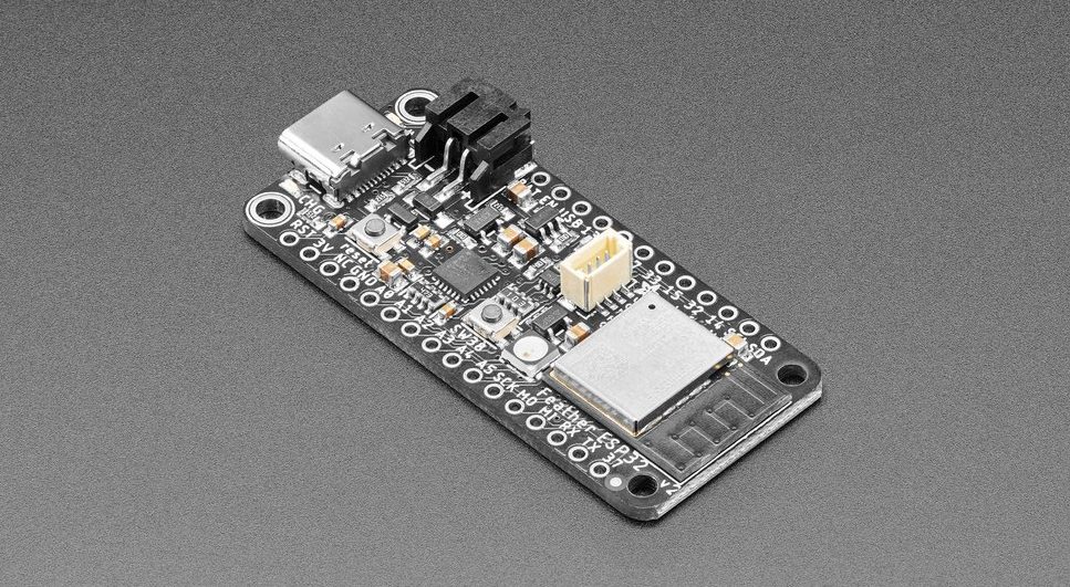
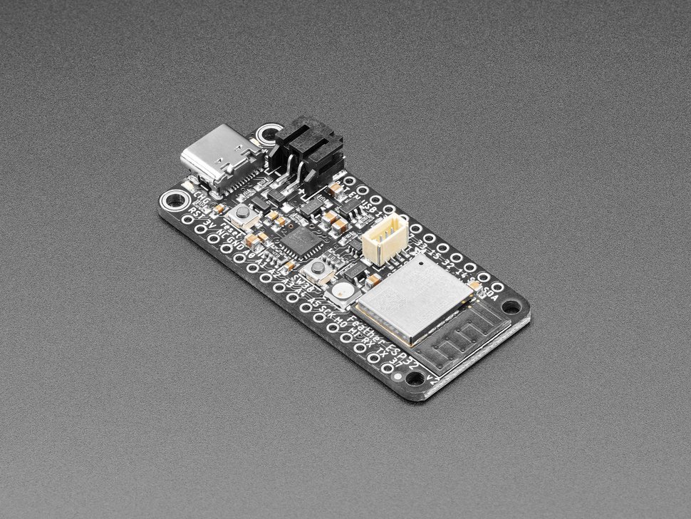
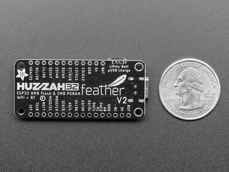
For over four years, we have seen the success of the Adafruit HUZZAH32 Feather board, which is still available for purchase on the Adafruit e-store. With its success comes the need to refresh and redesign to provide more functionalities to the board. Similarly, but not, in particular, Adafruit came across a problem with out-of-production Silicon Labs’ CP2104 highly integrated USB-to-UART bridge controller. Starting from here, the team ended up redesigning the full PCB and releasing version 2.0 of the original Adafruit HUZZAH32 Feather board– Adafruit ESP32 Feather V2.
Other than replacing Silicon Labs’ CP2104 with CP2012N USB-to-UART bridge controller, the new ESP32 board will feature an upgraded 8MB flash storage and 2MB PSRAM. The original Feather board had no PSRAM and limited 4MB of flash storage, which is seen as one of the major improvements. Adding a user button tactile switch, NeoPixel mini RGB LED, STEMMA QT port are seen as essential enhancements. STEMMA QT is a 4 pin JST SH, as a smaller 1.0mm pitch connector using I2C communication for plug and play capabilities to interface external modules and sensors. To reduce the power consumption for external sensors, there is a separate controllable 3V3 power supply for the STEMMA QT.
At the heart of the Adafruit ESP32 Feather V2 comes the ESP32 Pico Mini module featuring the classic ESP32 dual-core Xtensa processor with an adjustable clock frequency of 80 to 240MHz.
“The chip also has a low-power coprocessor that can be used instead of the CPU to save power while performing tasks that do not require much computing power, such as monitoring of peripherals.”
The ESP32 Pico Mini module also supports wireless connectivity of 2.4GHz Wi-Fi and Bluetooth with the BLE module. The bit rate for Wi-Fi 802.11n is up to 150 Mbps and the center frequency range of the operating channels is 2412 to 2484 MHz.
In terms of peripherals, the module supports an SD card slot for expanding storage and serial communication such as UART, SPI, and I2C. Others include LED PWM, Motor PWM, I2S, IR, pulse counter, GPIO, capacitive touch sensor, ADC, DAC, two-wire automotive interface, and Ethernet MAC. The favorite power supply mode of the USB Type-C port is brought onto the new Adafruit ESP32 Feather V2 instead of the USB Micro B present on the original Adafruit HUZZAH32. Other power options include the LiPoly battery that has two 200k resistor dividers and built-in battery charging when powered over a USB Type-C port.
Analysis
Complete redesign of the Adafruit HUZZAH32 Feather board looks interesting for low-power IoT applications such as video streaming, speech recognition, image recognition, home automation, smart agriculture, and wearable electronics. With all the major improvements from the onboard module to flexibility in power supply options, the manufacturer has given more customizable features for the developers to choose from. Also, the onboard STEMMA QT port has given added functionalities to interface hundreds of new modules and sensors to design applications that were never done before.
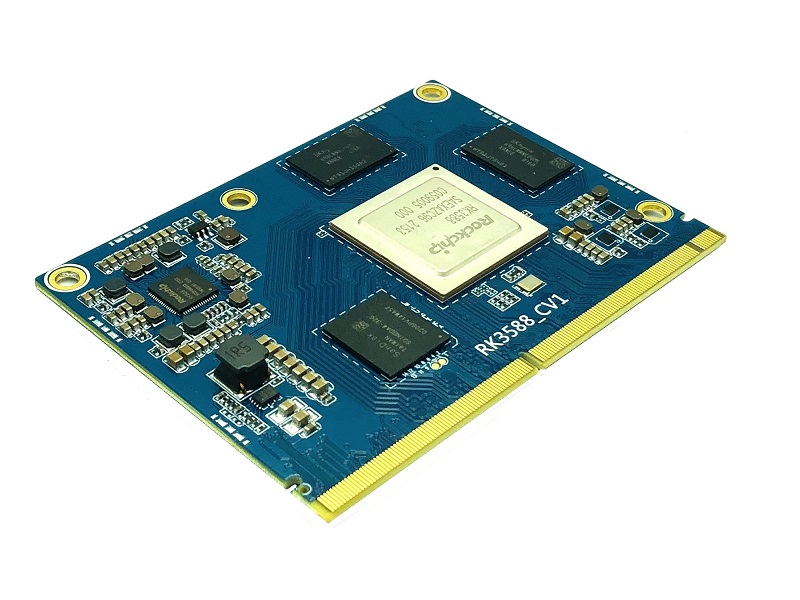
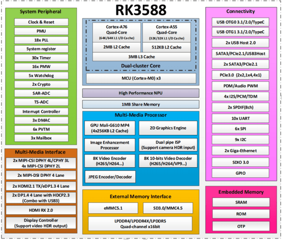
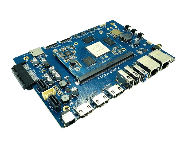
In simple terms, system-on-module (SoM) is an integrated printed circuited board with core components consisting of processor cores, communication interfaces, and memory blocks etc. Famously known as the Raspberry Pi (RPi) Compute Module (CM) is an SoM that can be interfaced on a suitable carrier board depending on the target applications. Similar to the RPi CM, Banana Pi has unveiled a new system-on-module integrated with the Rockchip RK3588 and requires a carrier board for input/output interfaces.
Rockchip RK3588 is a low-power, high-performance processor for edge computing devices that integrated a quad-core Cortex-A76 and a quad-core Cortex-A55 processor core with a separate NEON co-processor. The Arm Cortex-A76 has a big CPU cluster for high performance and the Arm Cortex-A55 has a smaller cluster that is optimized for low power. For image signal processing, the SoC comes with a hardware-focused 48-MP ISP to implement algorithms such as HDR, 3A, LSC, 3DNR, sharpening, fisheye correction, gamma correction and many more.
In terms of video processing, the hardware will provide optimized high-performance through the support for H.265 and VP9 decoder by 8K at 30/60 frames per second, H.264 decoder by8K at 30/60 frames per second and AV1 decoder by 4K at 60 frames per second. The embedded ARM Mali-G610 GPU makes the hardware compatible with OpenGLES 1.1, 2.0 and 3.2, OpenCL up to 2.2 and Vulkan 1.2. The built-in NPU has a computing power of up to 6TOPs supporting a series of frameworks such as TensorFlow, MXNet, PyTorch, and Caffe.
For high-performance, the system-on-module will support a range of LPDDR4 RAM– 2GB, 4GB, and 8GB, while for eMMC flash storage, you can get 32GB, 64GB, and 128GB options. The top version with 8GB LPDDR4 RAM and 128GB storage will make the SoM outperform many of the existing boards in the market, making it optimum for high-end edge computing applications. To provide all the I/O connections, the SoM will fit on the carrier board that will be shipped with 3x HDMI ports (possible 2x for video output and 1x for video input), 1x USB 3.1 port, 2x USB 2.0 ports, 1x USB Type-C port, and a MicroSD card slot. For interfacing camera and display, there is MIPI CSI and DSI interfaces while for increasing the storage, a horizontal PCIe slot is present.
We don’t have a clear picture about wireless connectivity, however, CNX-Software notes that
“I can also see what looks like WiFi + Bluetooth module plus three u.FL antenna connectors.”
On the software side, Banana Pi will provide Android 12.0 and Linux BSPs for the RK3588 SoM and development kit.
Analysis
As one of the latest Rockchip SoC, it was obvious to see an SoM with Rockchip RK3588 system-on-chip, unlike, we recently covered the Orange Pi 4 LTS design that comes with the early Rockchip RK3399 SoC. For a long-time, after the release of RK3588 SoC there was no datasheet and intricate information on the CPU and GPU benchmarks, but at the Rockchip Developer Conference 2021, the manufacturer provided more information as spotted by CNX-Software. This gives us a sense of understanding that Rockchip expects more attention around the RK3588 system-on-chip, as recently we witnessed Radxa Rock5 Model B.
At the end of the announcement, Banana Pi claims the hardware samples to be ready, but the BSP is still in the development process. Understanding the complex RK3588 system-on-chip, we are expecting a decently more time for the hardware to hit the market with the earliest being Q3/Q4 2022. Since it’s a long way from the market launch, we do not have any information on the pricing.
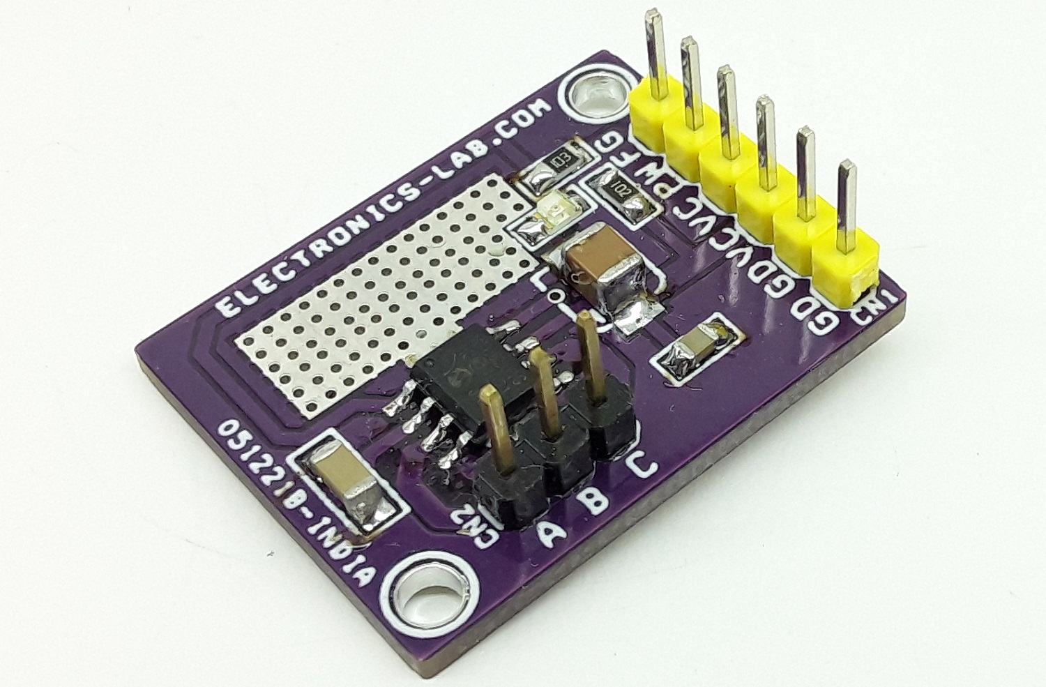
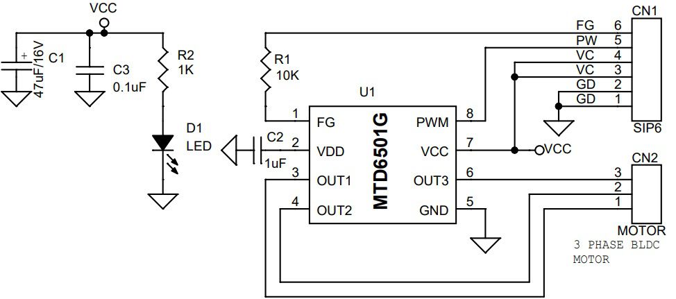
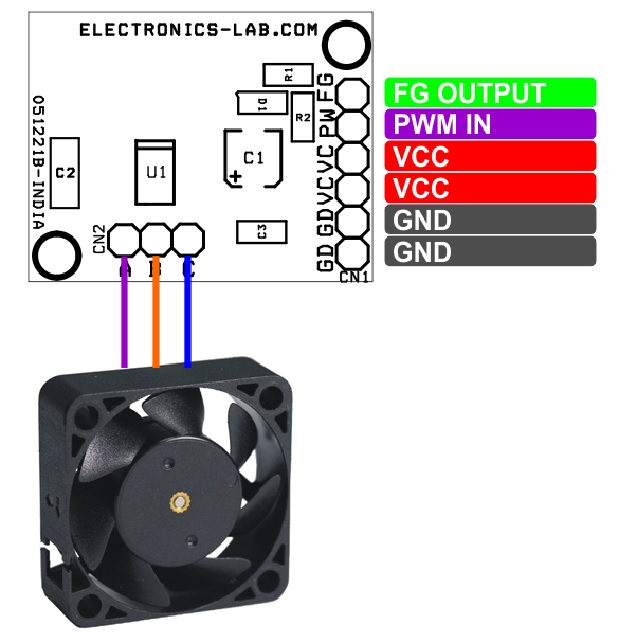
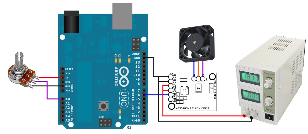
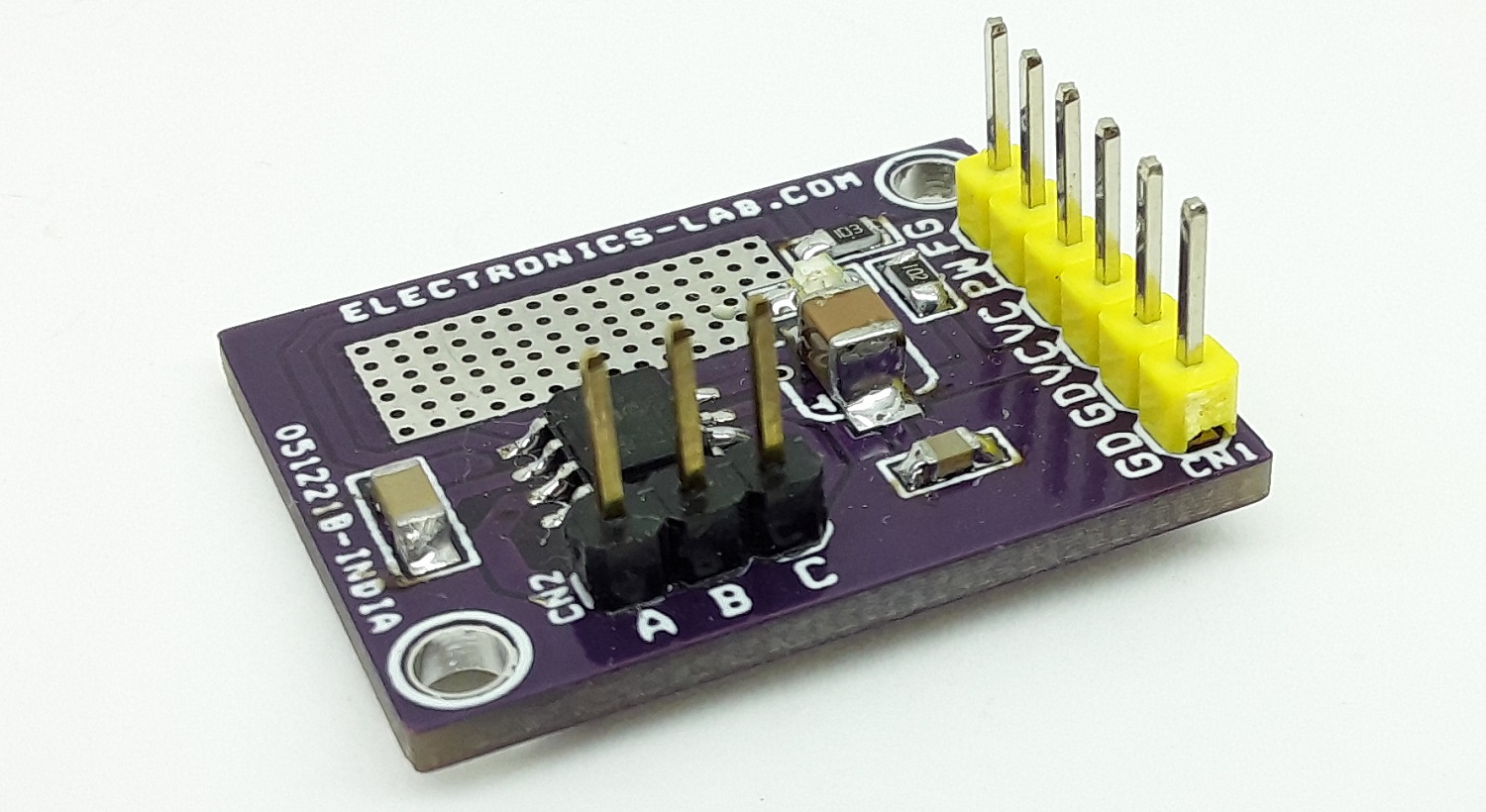
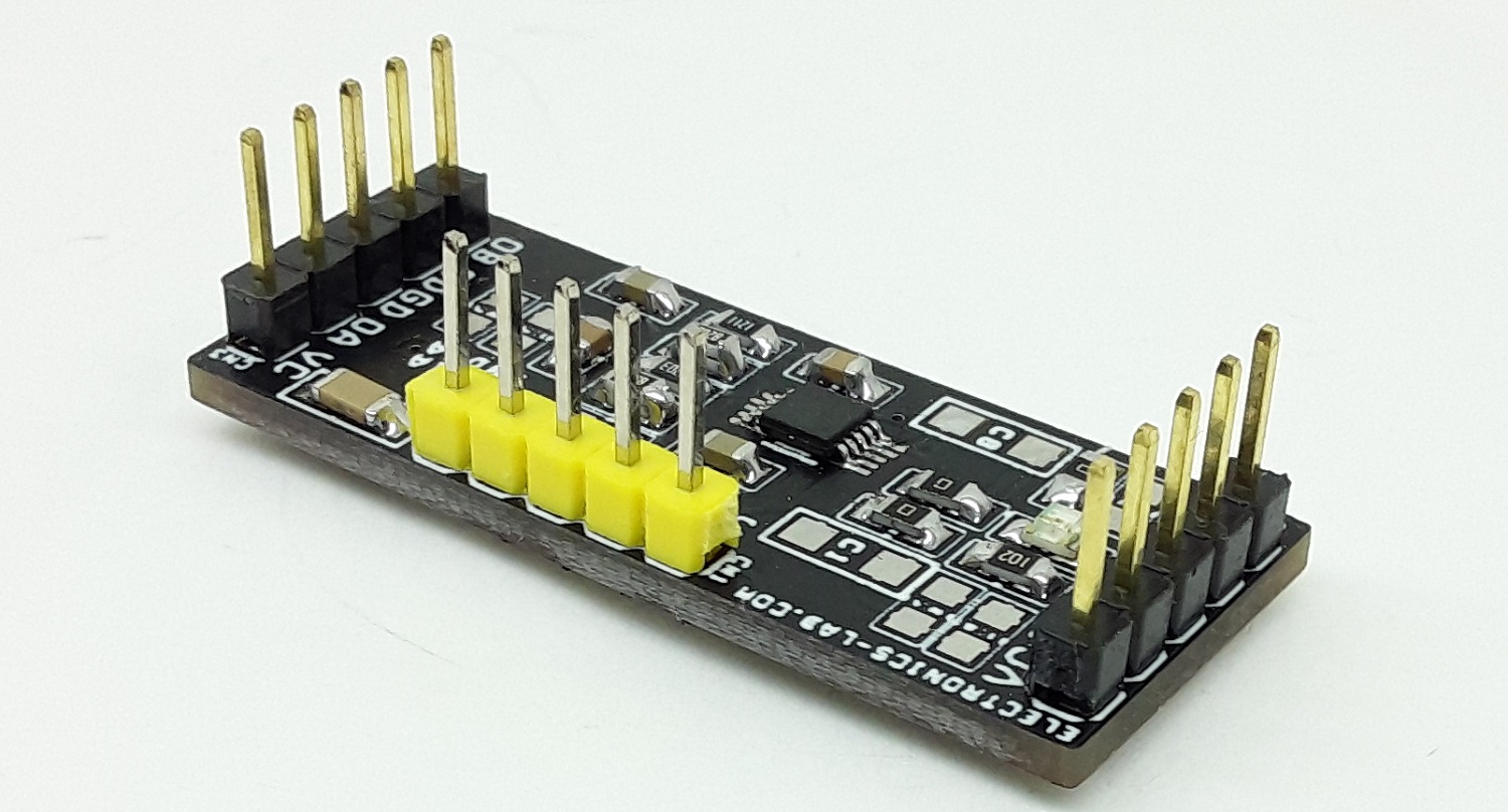
Driving a low current 3 phase brushless Sensorless DC motor is very easy with this project. This Full-wave BLDC driver project is capable to drive low current brushless fan motor without a hall sensor. 180° sinusoidal drive, high torque output, and silent drive are a few key features of the project. Due to their adaptive features and wide power-supply range capabilities (3 to 12V) they are intended to cover a wide range of motor characteristics while requiring no external tuning from the user. Speed control can be achieved through either power supply modulation or pulse-width-modulation (using the PWM digital input pin5 of CN1). Due to the compact packaging and minimum bill-of-material (power transistors incorporated, no Hall sensor, no external tuning), the project is best suited for low-cost fan applications requiring high efficiency and low acoustic noise, such as CPU cooling fans. The frequency generator output is also included, enabling precision speed control in closed-loop applications. Motor over-current limitation, short-circuit protection, and thermal shutdown protection is also included. Connect 3 Phase Motor to CN2, Apply Motor Supply to GND and VCC of CN1, Apply PWM signal to PIN 5 of CN1. D1 Power LED.
Connections CN1
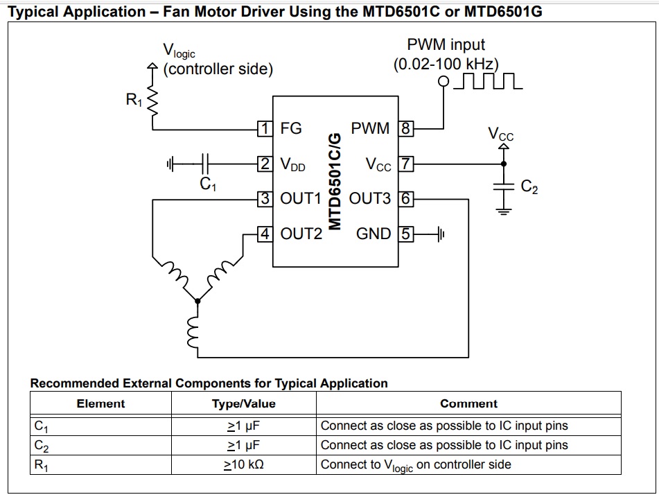
Pin 6: FG Frequency Generator Output (Feedback Signal Output)
Pin5: PWM Signal Input (Frequency 20Hz to 100Khz, Duty Cycle 0 to 100%)
Pin4: VCC 3V to 12V DC Positive
Pin3: VCC 3V to 12V DC Positive
Pin 2: GND
Pin1: GND
Connector CN2: 3 Phase Brushless Motor
Note: This project has been tested using Arduino as PWM generator, follow the connection diagram for connections. Example Arduino code available as a download.
Features
Supply 3V To 12V DC (Range 2V To 14V DC)
Maximum Output Current 800mA
Output Frequency 23Khz
Position Sensorless BLDC drivers (no Hall sensor required)
180° sinusoidal drive, for high efficiency and low acoustic noise
Speed control through PAM and/or PWM
Built-in frequency generator
Built-in lockup protection and automatic recovery circuit (external capacitor not necessary)
Built-in overcurrent limitation and short circuit protection
Built-in thermal shutdown protection
No external tuning required
PCB Dimensions 27.94 x 21.59mm
Speed Control (CN1 Pin 5)
The rotational speed of the motor can be controlled either through the PWM digital input signal or by acting directly on the power supply (VCC). When the PWM signal is “High” (or left open) the motor rotates at full speed. When the PWM signal is “Low”, the motor is stopped (and the IC outputs are set to high impedance). By changing the PWM duty cycle, the speed can be adjusted. Notice that the PWM frequency has no special meaning for the motor speed and is asynchronous with the activation of the output transistors. Thus, the user has maximum freedom to choose the PWM system frequency within a wide range (from 20 Hz to 100 kHz), while the output transistor activation always occurs at a fixed rate, which is outside of the range of audible frequencies. The MTD6501G output frequency is 23 kHz.
FG -Frequency Generator Function (CN1 Pin 6)
The Frequency Generator output is a “Hall-sensor equivalent” digital output, giving information to an external controller about the speed and phase of the motor. The FG pin is an open drain output, connecting to a logical voltage level through an external pull-up resistor. When a lock (or out-of-sync) situation is detected by the driver, this output is set to high-impedance until the motor is restarted. Leave the pin open when not used. The FG signal can be used to compute the motor speed in rotations per minute (RPM). Typically, for a four pole BLDC fan, the speed in RPMs is 30 FG frequency (Hz)
Lockup Protection and Automatic Restart
If the motor is stopped (blocked) or if it loses synchronization with the driver, a lock-up protection circuit detects this situation and disables the driver (by setting its outputs to high-impedance) in order to prevent the motor coil from burnout. After a “waiting time” (TWAIT), the lock-up protection is released and normal operation resumes for a given time (TRUN). In case the motor is still blocked, a new period of waiting time is started. TWAIT and TRUN timings are fixed internally, so that no external capacitor is needed.
Overcurrent Protection and Short Circuit Detection
The motor peak current is limited by the driver to a fixed value (defined internally), thus limiting the maximum power dissipation in the coils. The detection of a short-circuit situation immediately sets the driver outputs to high-impedance, in order to avoid permanent damage to the IC
Thermal Shutdown
The MTD6501G Chip have a thermal protection function which detects when the die temperature exceeds TSD = +170°C. When this temperature is reached, the circuit enters Thermal Shutdown mode and the outputs OUT1, OUT2 and OUT3 are disabled (high-impedance), avoiding IC destruction and allowing the circuit to cool down. Once the junction temperature (TSD) has dropped below +145°C, the normal operation resumes (thermal detection circuit has +25°C hysteresis function).
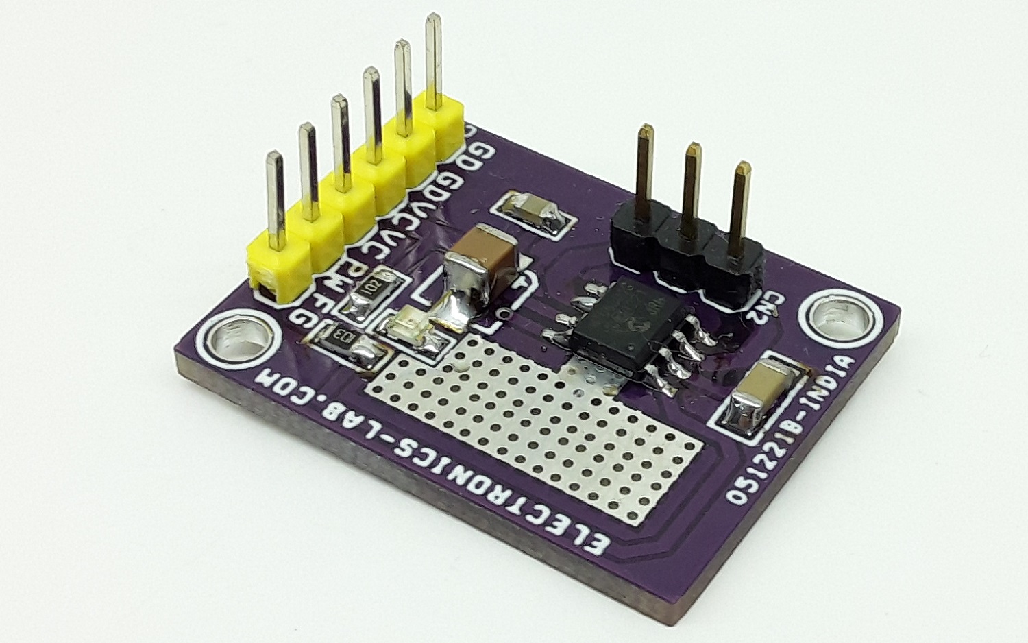
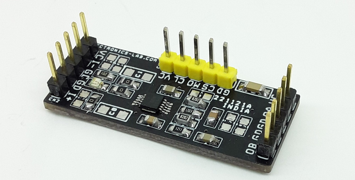
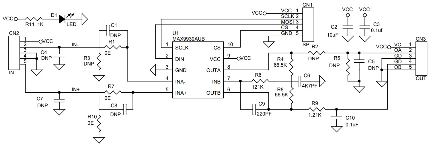
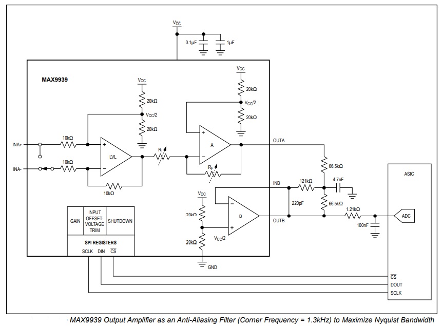
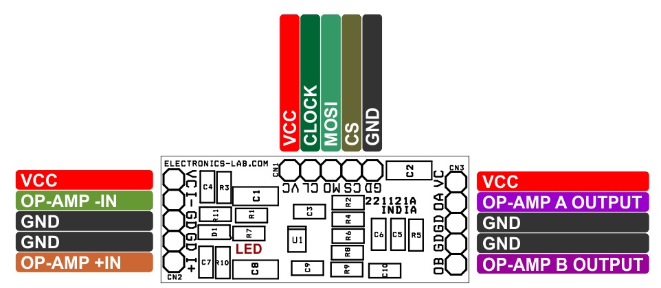
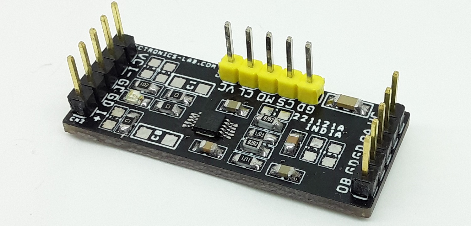
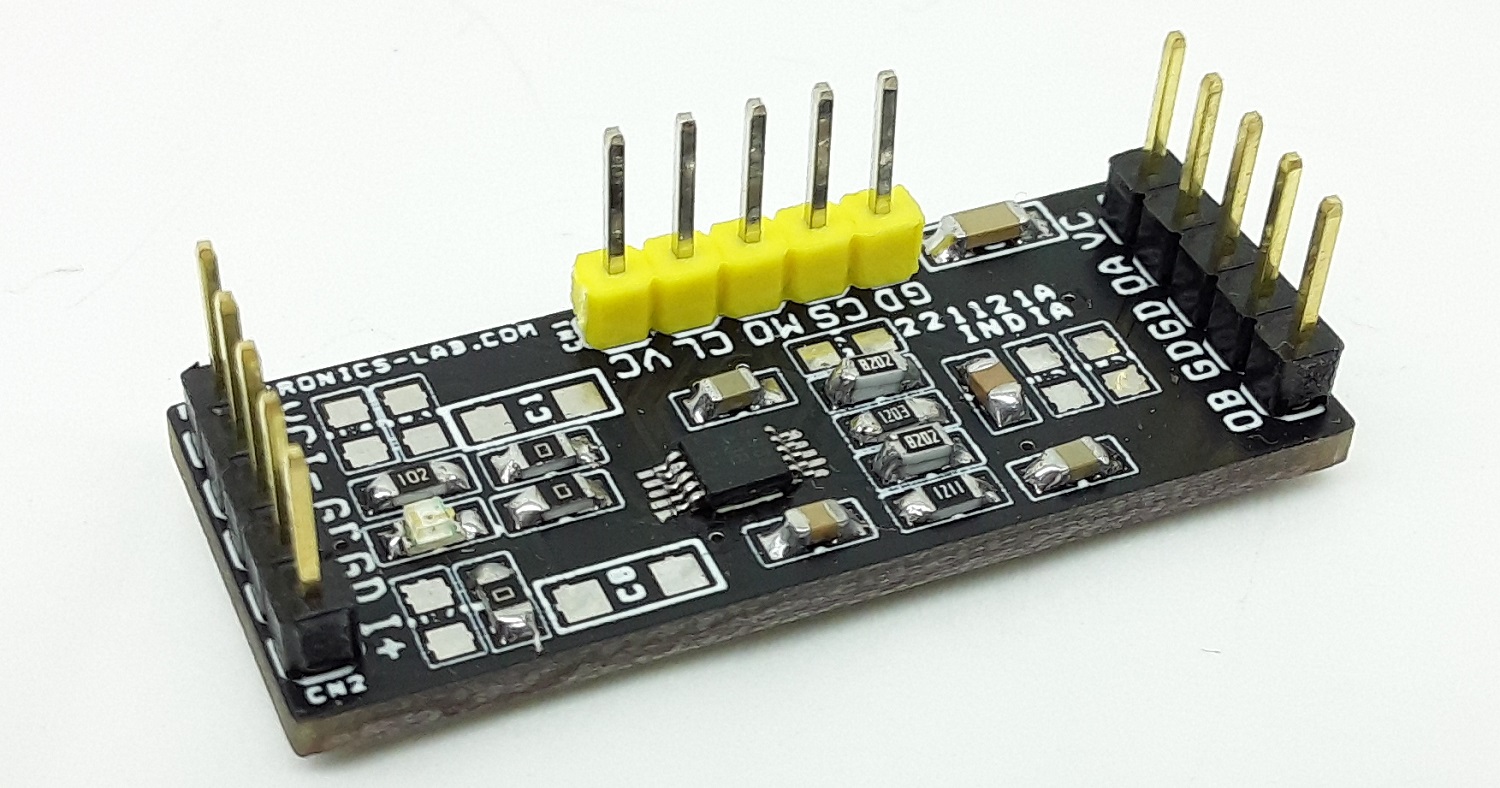
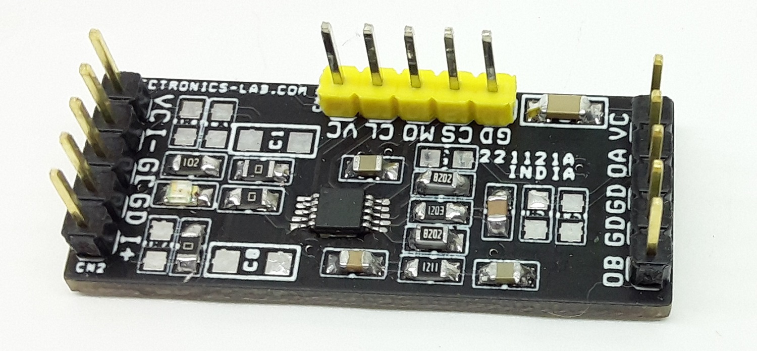
The project presented here is an SPI programable Gain Amplifier using MAX9939. The MAX9939 is a general-purpose, differential-input programmable-gain amplifier (PGA) that is ideal for conditioning a variety of wide dynamic range signals such as those found in motor current-sense, medical instrumentation, and sonar data acquisition applications. It features SPI-programmable differential gains from 0.2V/Vto 157V/V, input offset-voltage compensation, and an output amplifier that can be configured either as a high-order active filter or to provide a differential output.
The PGA is optimized for high-signal bandwidth and its gain can be programmed to be 0.2V/V, 1V/V, 10V/V, 20V/V, 30V/V, 40V/V, 60V/V, 80V/V, 119V/V, and 157V/V. Precision resistor matching provides extremely low gain tempco and high CMRR. Although the MAX9939 operates from a single supply VCC between 2.9V to 5.5V, it can process signals both above and below ground due to the use of an input level-shifting amplifier stage. Furthermore, its inputs are protected to ±16V, allowing it to withstand fault conditions and signal overranges. The output amplifier is designed for high bandwidth and low-bias currents, making it ideal for use in multiple-feedback active filter topologies that offer much higher Qs and stopband attenuation than Sallen-Key architectures. The MAX9939 draws 3.4mA of quiescent supply current at 5V, and includes a software-programmable shutdown mode that reduces its supply current to only 13µA.
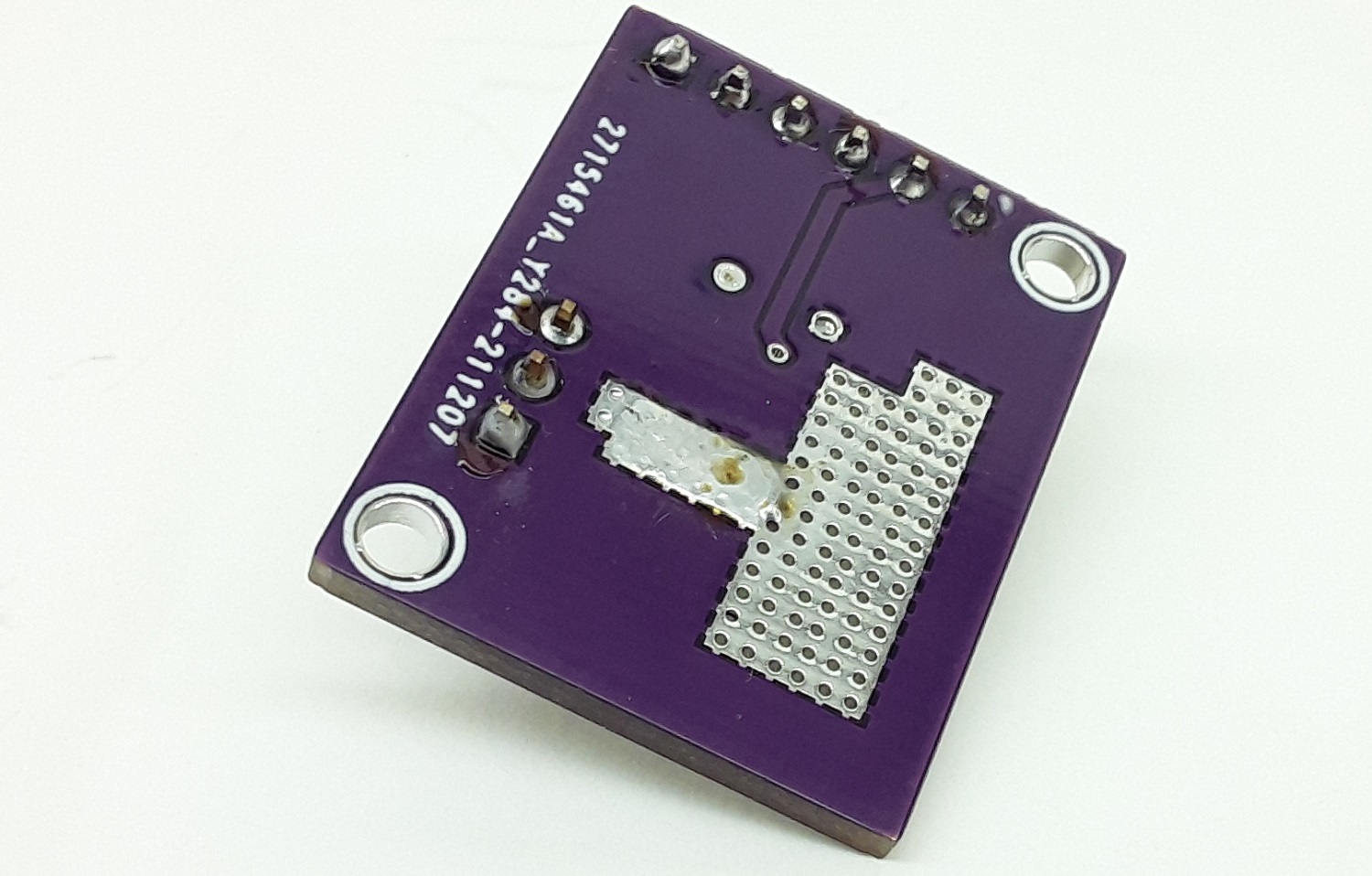
Note: This is a general-purpose SPI programable gain amplifier, all components are user-defined, capacitors and resistors value as per application. Refer to the datasheet of the chip for more information.
Key Features
Operating Power Supply 3V to 5V DC
SPI-Programmable Gains: 0.2V/V to 157V/V
Extremely Low Gain Tempco
Integrated Amplifier for R/C Programmable Active Filter
The switching theory uses switches in order to understand the operation and functioning of digital logic gates and circuits. The switching theory helps in developing better theoretical knowledge and concepts of digital logic circuits involving logical inputs producing a specific relational logical output. As it has already been discussed that Boolean data type has only two distinctive states i.e. “0” or “1”. They are also referred to as “LOW” and “HIGH” or “OFF” and “ON”, respectively. Digital logic input and output can have only these two states. A switch or an electromechanical contact of a relay also has only two distinctive states i.e. “OFF” or “ON”. Therefore, a digital logic input or output can be represented by a physical switch, and Boolean Algebra laws, rules, and theorems can be applied to them. The Boolean expressions can be expressed by switching theory which eases the understanding of digital logic gates.
The understanding of digital logic gates is essential when dealing with complex logic circuits or microprocessors. The digital logic gates are the basic building blocks of combinational and sequential logic circuits. The combinational logic circuits are dependent on only external inputs or signals applied to them. Whereas, the sequential logic circuits are dependent on the present state, its output, and externally applied inputs.
Theory of a Switch
A switch can be thought of as a wall switch which is normally found in households to turn “ON” or “OFF” a light/ lamp. A switch can also be an electromechanical contact of a relay to allow the flow of current in either direction.
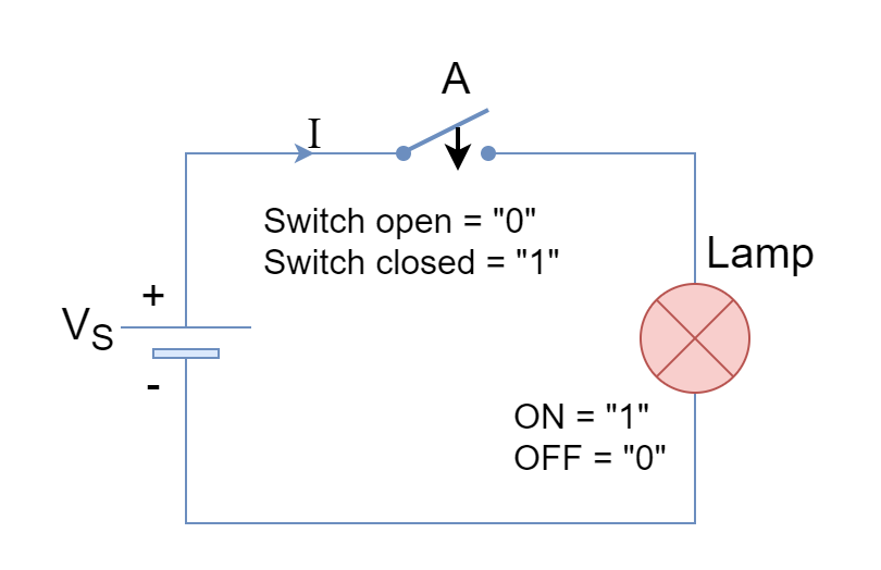
A Normally-open Switch
In the following circuit, a voltage source is connected to a lamp through a normally-open switch. Under normal conditions i.e. the switch is open, the electric path between the voltage source and the lamp is not established and no current flows. The lamp does not glow or illuminate. However, when the switch is pressed i.e. switch closed, the electric path between the voltage source and the lamp gets established. A current flows to the lamp from the voltage source through the switch and illuminates the lamp.
Figure 1: A normally-open switch
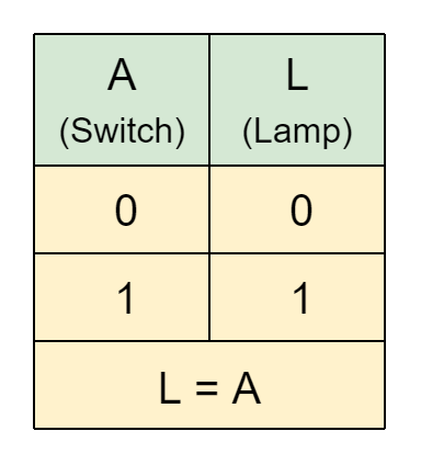
The switch positions i.e. “OFF/ OPEN” and “ON/ CLOSED” are equivalent to Boolean states of “0” and “1”, respectively. Likewise, lamp states of “OFF” and “ON” by “0” and “1”, respectively. The switch can be represented by an input (A) and lamp as an output (L).
When the switch/ input (A) is open “0” then the lamp/ output (L) is also “0” or not illuminated. Likewise, when the switch/ input (A) is closed “1” then the lamp/ output is “1” or illuminated. This can be illustrated by the equivalent switching truth table which is shown below.
From the above table, the switch equals lamp i.e. A = L which means that when the switch is “OFF” the lamp will also be “OFF” and this phenomenon holds under the “ON” state of the switch. The switch used in the above circuit is normally-open and it has to physically make a contact to be considered closed. The other type of switch is normally closed which is opposite of normally open and has to physically break the contact in order to be considered open.
A Normally-closed Switch
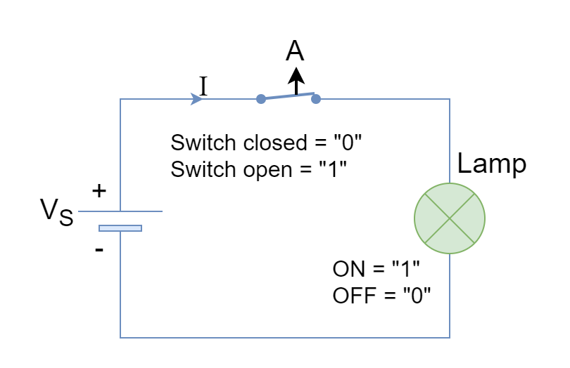
In the following circuit, a voltage source is connected to a lamp through a normally-closed switch. Under normal conditions i.e. switch is closed, the electric path between voltage source and lamp is established and current flows to illuminate the lamp. However, when the switch is pressed i.e. switch open, the electric path between the voltage source and lamp breaks. The current flow along with the illumination of the lamp stops.
Figure 2: A normally-closed switch
Here, the switch positions i.e. “OFF/ OPEN” and “ON/ CLOSED” are equivalent to Boolean states of “1” and “0”, respectively.
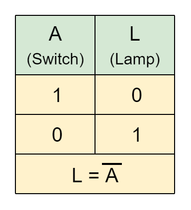
The above electric circuit can be described as when the switch/ input (A) is open “1” then lamp/ output (L) is “0” (not illuminated). Likewise, when the switch/ input (A) is closed “0” then the lamp/ output is “1” (illuminated). This can be illustrated by the equivalent switching truth table which is shown below.
From the above table, the switch and lamp states are opposite to each other which means that when the switch is “OFF” the lamp will be “ON” and, likewise, when the switch is “ON” the lamp will be “OFF”. The normally-closed switch is performing the inversion function in terms of switching theory.
Series Switches Case
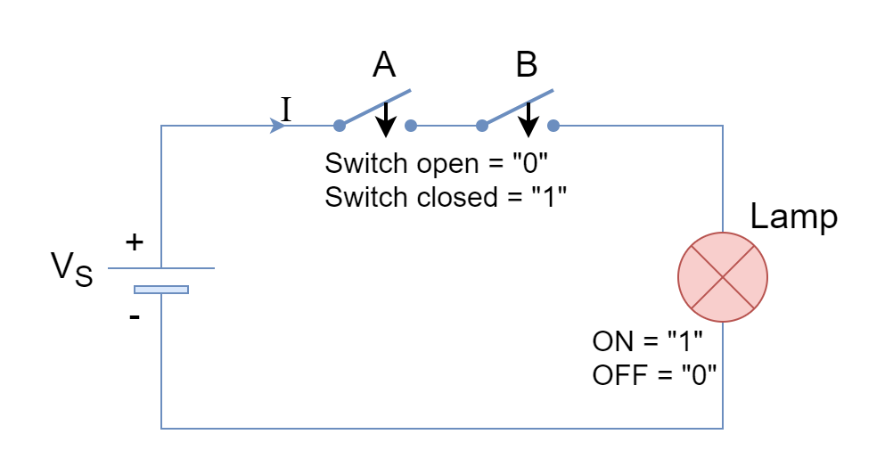
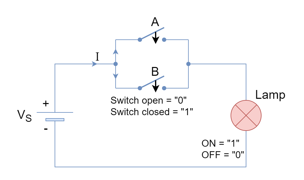
In the above circuit, a single switch is used to control the lamp operation. The single switch allowed the flow of current to the lamp in order to illuminate it. The state of a single switch is equivalent to lamp state i.e. both are “OFF” or “ON” at the same time. The addition of a switch in series with the first switch leads to a different state of affairs.
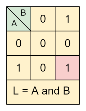
Consider the following circuit having a voltage source, a lamp, and two series switches. The switches can be labeled as inputs “A” and “B”. There open/ off states are represented by “0” and closed/ on states by “1”. The two switches make a total of four combinations to control the lamp. The first combination is A=0 & B=0, the second combination is A=0 & B=1, the third combination is A=1 & B=0, and the fourth combination is A=1 & B=1. The lamp has four states corresponding to each combination of A and B. As obvious from physical switches in series, the current will flow from the voltage source to the lamp when both switches are closed or at a logical “1” state. The series switches’ truth table is shown below:
Figure 3: A series switches case
From the following truth table, it is clear that when both switches/ inputs are closed or at “1” logical state then the lamp illuminates (state of “1”). When either of the switches is at the “0” logical state, the lamp is at the “0” state. This leads to L = A and B expression. In Boolean Algebra, it is an AND logical operation which is denoted by a single dot (.) between the input variables i.e. L=A.B.
Hence, in the switching theory and operation of series switches is equivalent to a digital logic “AND” gate.
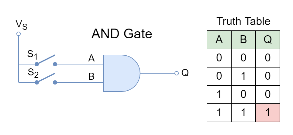
Digital Logic AND Gate
The switching theory equivalent logic AND gate is shown below along with its truth table. The switches “A” and “B” are AND’ed together to yield an output “Q”.
Figure 4: The switching AND gate and truth table
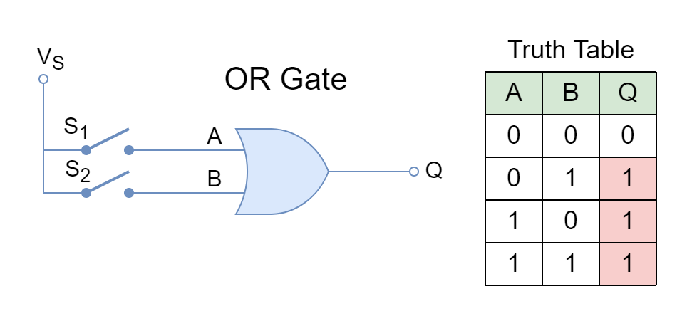
Parallel Switches Case
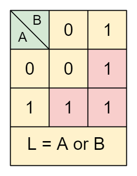
Consider the following circuit having a voltage source, a lamp, and two parallel switches. Similar to the series switches, these two parallel switches make a total of four combinations to control the lamp. The lamp has four states corresponding to each combination of A and B which are now connected in parallel to each other. As obvious from physical switches in parallel, the current will flow from the voltage source to the lamp when any of the switches is in a closed or at a logical “1” state. The parallel switches’ truth table is shown below:
Figure 5: A parallel switches case
From following the truth table, it is clear that when both switches/ inputs are open or at a “0” logical state then the lamp does not illuminate (state of “0”). When either of the switches is closed or at a “1” logical state, the lamp illuminates (a “1” state). This leads to L = A or B expression. In Boolean Algebra, it is an OR logical operation that is denoted by a plus (+) between the input variables i.e. L=A+B.
Hence, in the switching theory and operation of parallel switches is equivalent to a digital logic “OR” gate.
Digital Logic OR Gate
The switching theory equivalent logic OR gate is shown below along with its truth table. The switches “A” and “B” are OR’ed together to yield an output “Q”.
Figure 6: The Switching OR gate and truth table
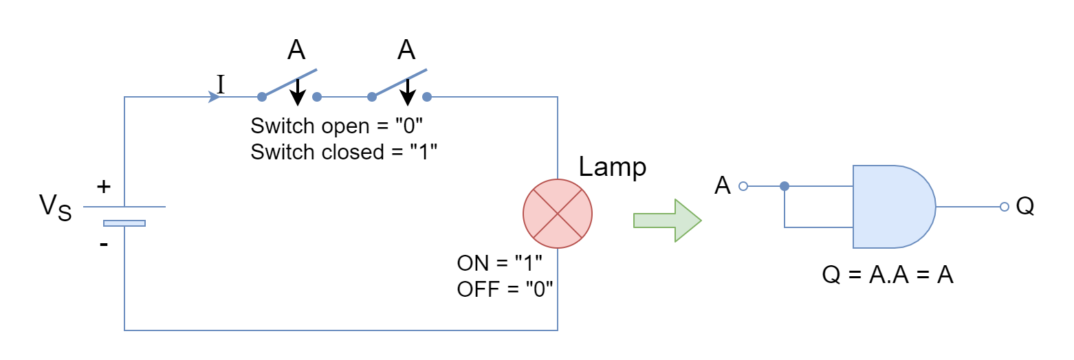
Idempotent Law of Switches
In the above text, the switching theory equivalent logical AND, and OR gates are discussed having two different switches or variables i.e. “A” and “B”. These two variables can be controlled by a single variable such as “A” and operation of logical AND, and OR on single variables is defined as Idempotent Law. According to Idempotent Law, the AND’ing or OR’ing of a variable with itself will yield the original variable. This means that “A” OR’ed with “A” will yield “A” and, likewise, AND operation will also yield “A”. This can simplify switching circuits as illustrated below.
Idempotent Law of AND Function
The electric circuit constituting of same series switches along with the switching theory equivalent of AND gate is shown below.
Figure 7: Idempotent AND equivalent of switches
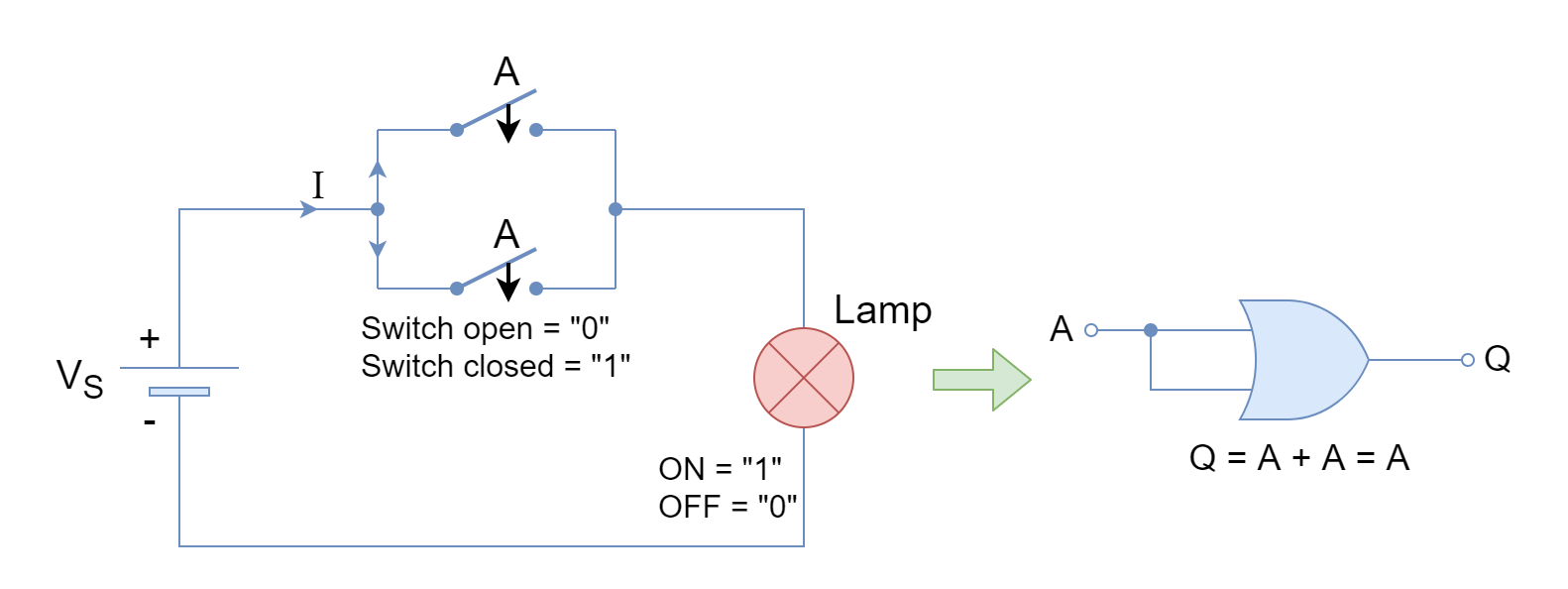
Idempotent Law of OR Function
The electric circuit constituting of same parallel switches along with the switching theory equivalent of the OR gate is shown below.
Figure 8: Idempotent OR equivalent of switches
Switching theory of a Boolean Function
According to switching theory, a combination of series switches gives a logical AND (multiplication) operation which is denoted by a dot (.) between variables. Similarly, a parallel combination of series switches gives a logical OR (sum) operation which is denoted by a plus (+) between variables. Using these switching theory equivalents a Boolean function can be constructed from an electric circuit and vice versa.
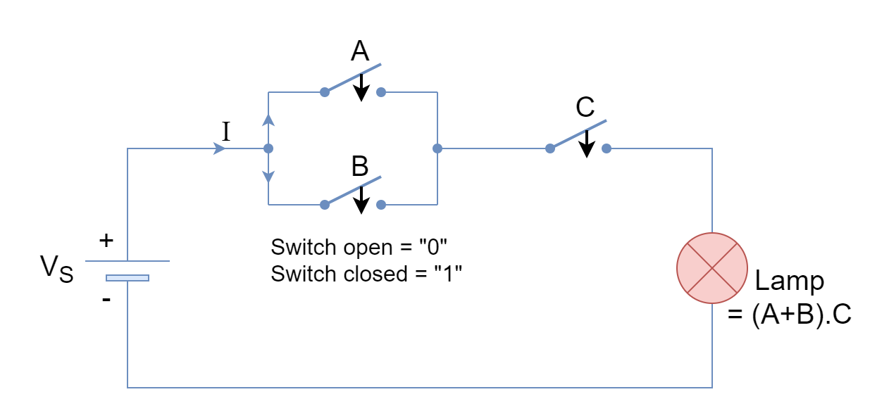
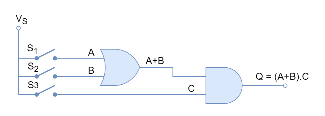
Switching Theory Example
In the following figure, a Boolean function of Q = (A+B).C is implemented using switches to illuminate a lamp (Q). Likewise, a Boolean function can also be obtained from a switching circuit using switching theory.
Figure 9: Example of switching theoryFigure 10: The logic equivalent of the example switching circuit
Conclusion
A switch can be used to express a digital state of input i.e. “OFF” equals “0” and “ON” equals “1”.
The switching theory expresses Boolean expressions in terms of switches to help in understanding.
The switches in series illuminate the lamp when both are “CLOSED” or “1” and constitute a logical AND operation.
The switches in parallel illuminate the lamp when any of them is “CLOSED” or “1” and constitute a logical OR operation.
Using switching theory, any Boolean expression can be used to construct a switching circuit and, likewise, a switching circuit’s equivalent Boolean expression can also be derived.
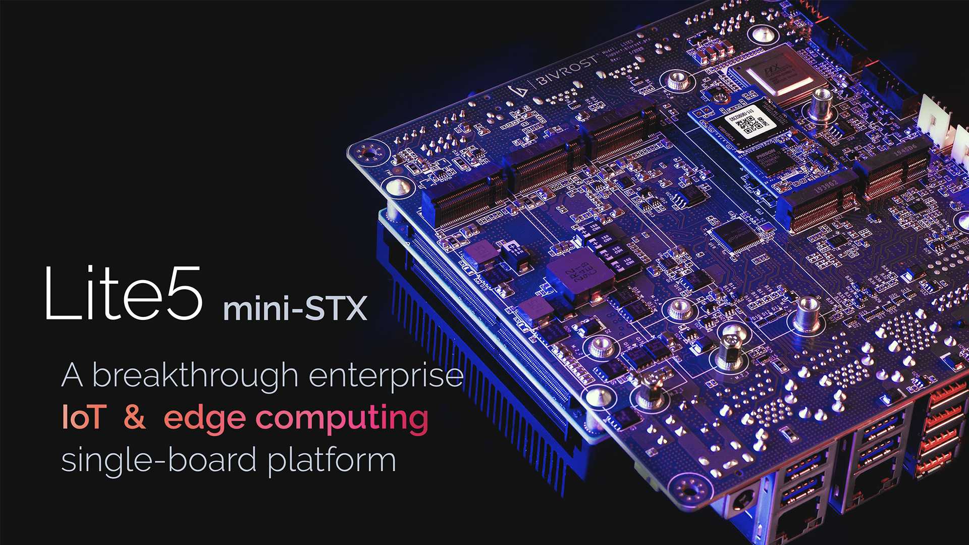
BIVROST® Lite5 is an extremely compact industrial computer that breaks through I/O bandwidth barriers for the most demanding applications, including machine vision and the edge computing work model based on neural network accelerators. Using Intel Xeon and Intel Core processors and supporting 5 M.2 slots, only 5 inches in size (mini-STX standard), the data processing capabilities found in enterprise-class solutions were compressed.
BIVROST® Lite5 platform is a combination of a universal motherboard with carrier-board characteristics with a module in the COM Express architecture (Basic Module Type 6), on which the processor and operating memory are embedded. This solution ensures a long project life, increase fault tolerance, and reduce the costs of migrating to newer processors in the future. By default, the Intel Core i7-8850H processor (6 cores / 12 threads, 2.6 GHz – 4.3 GHz, 9 MB cache, 45 W TDP) is offered along with 16/32/64/96 GB DDR4 memory. The 8th and 9th generations of Intel embedded processors are supported, and the 11th and 12th generation will join this year.
The essence of BIVROST® Lite5 is to provide extreme capacity on all available I/O interfaces used in industry. Of the five available M.2 slots, three are high-throughput M-key, providing a transfer rate of 32 Gbps (size 2280, PCIe 3.0 x4 lines). They enable the installation of neural network (AI) accelerators based on Intel, Coral, Hailo systems or fast and independent NVME disks. The independent speed of the slots allows the use of video capture cards or individual specialized FPGAs embedded on the M.2 interface.
The Lite5 project was born out of our own need. The design challenge was the necessity to connect multiple industrial cameras Pixelink (Navitar) with 8Gbps data capacity each simultaneously, image analysis using a neural network model on a dedicated accelerator and simultaneous recording of this data. And all to increase the efficiency and reliability of the automated production line. Due to information security, the project had to be free from cloud data analysis, work 24/7 and offline.
says Paweł Surgiel, President of the Management Board of BIVROST Sp. z o.o.
The Lite5 provides a wide range of input-output interfaces, including GPIO, I2C, LVDS, USB (3.2 gen2, 3.2 gen1, 2.0), UART, M.2 (key B, key E, key M), HDMI 2.0. The special 4 USB slots in the 3.2 gen2 standard provide a guaranteed total bandwidth of 32 Gbps thanks to the use of independent root hub chips and independent PCI Express lanes.
Key features:
Architecture: COM Express Type 6, extended support provided (embedded class)
CPU / GPU (default): Intel Core i7-8850H i Intel® UHD 630 GPU (6 cores, 12 threads, 2.6GHz – 4,3 Ghz, 45W / 35W CPU TDP)
Memory: 3 slots DDR4, max 96 GB, default 16 GB
I/O for embedded systems: GPIO, I2C, LVDS, 2x HDMI 2.0, SPDIF, 2x LAN 1Gbps
2: 3x universal (M key, size 2280, PCIe 3.0 x4 lanes), 1x SATA (B key), 1x WiFi (E key)
USB ports with dedicated, unshared bandwidth
Compact size: 5-inches (mini-STX),
Compatibility OS: Windows 10, Windows 11, Ubuntu Linux
BIVROST is the project leader. It was created by an international team with the support of Intel engineers, and the Taiwanese company Advantech is responsible for production. Technical support is provided in 24 countries. Lite5 is targeted at the most demanding industrial applications, especially in image analysis, as a runtime environment for neural network accelerators, in multimedia and digital signage projects, and in the security industry.
Portescap returns in person to Medical Design & Manufacturing West 2022 for the first time since 2020 to discuss the benefits of its medical motors, which power surgical hand tools, medical pumps, lab automation and ventilation equipment, and several other medical devices.
Portescap will demo its Surgical Motor Solutions — featuring sterilizable motors and controllers designed to withstand 3,000+ autoclave cycles — and showcase recent innovations. These include the CNT1530 sterilizable motor controller for surgical hand tools and new additions to its line of Ultra EC™ brushless DC motors.
With electronics and software encapsulated in a single enclosure, the CNT1530 provides simplified system integration. Compatible with typical NiMH and LiOn battery voltages, it features 20 amps of continuous current and can be paired with Portescap brushless DC slotted surgical motors.
New sizes have been added to the Portescap Ultra EC motor family. When targeted performance is critical, Ultra EC motors deliver minimal joule and iron losses while maintaining maximum power, thanks to a proprietary U coil design. Whether you require high speed, high torque or a balanced performance solution, Ultra EC motors are perfectly suited for medical and dental hand tools, respirators, robotics and more.
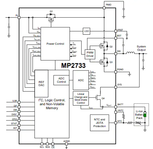
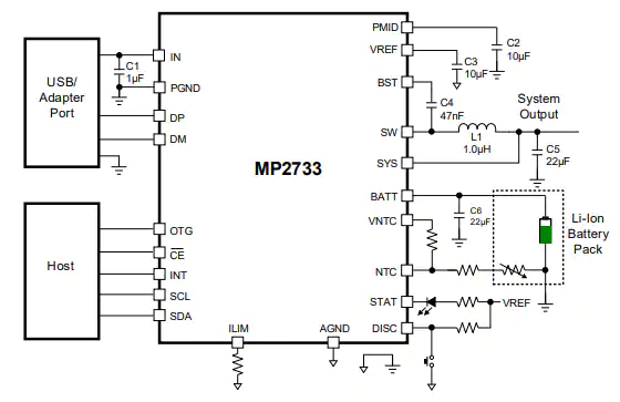
Monolithic Power Systems (MPS) MP2733 Battery Charger Management Devices are highly integrated switchmode battery charger management devices for single-cell Li-ion or Li-polymer batteries. These devices work with Narrow Voltage DC (NVDC) system power path management. The MP2733 devices feature a low-impedance power path that optimizes efficiency, reduces battery charging time, and extends battery life. These devices support a wide range of input sources, including standard USB host ports and high-powered wall adapters with fast-charge capabilities. The I2C interface allows the device to be flexibly controlled with configurable charging and system settings.
The MP2733 devices initiate and complete a charging cycle without software control. It automatically detects the battery voltage and charges the battery in different stages. Charging automatically terminates when a full charge is detected. When the charged battery drops below the recharge threshold, the charger automatically begins another charging cycle. These devices offer various safety features for battery charging and system operations, including a charging safety timer, battery temperature monitoring, Over-Voltage Protection (OVP), and Over-Current Protection (OCP). Typical applications include smartphones, tablets, wireless cameras, and other portable devices.
Features
3.7V to 16V operating input voltage range
Up to 22V sustainable voltage
High-efficiency, 4.5A, 1.35MHz buck charger with up to 92% charge efficiency with 3A charge current:
Configurable D+/D- for flexible fast charge protocol support
USB OTG with 4.8V to 5.5V adjustable output:
Up to 3A output and up to 93% efficiency with 1.5A output
NVDC power path management:
Instant-on works with no battery or deeply discharged battery
Ideal diode operation in battery supplement mode
High battery discharge efficiency with 14mΩ BATTFET up to 8.5A
I2C interface for flexible system parameter setting and status reporting
Fully integrated MOSFETs and current sensing
Dedicated DISC pin to control shipping mode and system reset
13µA low battery leakage current in shipping mode
Integrated ADC monitors input voltage and current, battery voltage, charge current, system voltage, and battery temperature
Charging status indicator
Safety features:
Configurable JEITA for battery temp protection in charge mode, battery charging safety timer, thermal regulation and shutdown, watchdog monitoring I2C, and input/system OVP
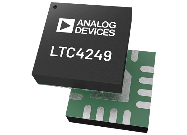
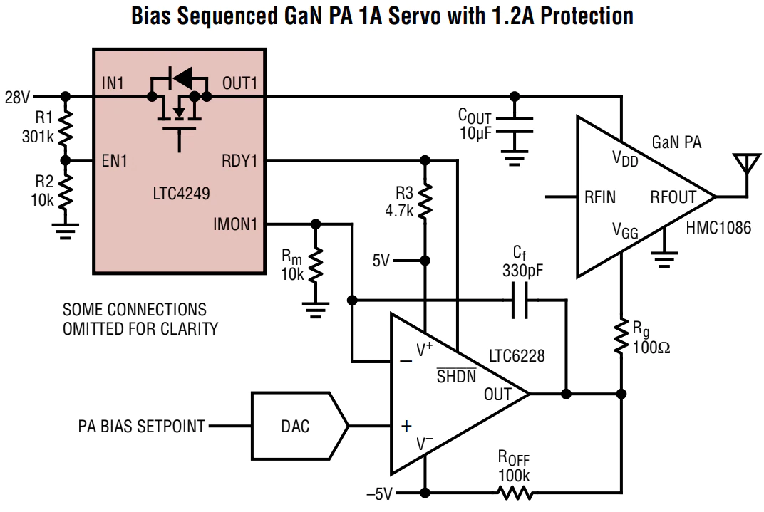
Analog Devices Inc. LTC4249 Dual Electronic Circuit Breaker (ECB) provides independent overcurrent protection to a pair of loads. Each channel has a precision enable input, current monitor output, and ready status output. A single resistor configures the ECB threshold. If either channel detects an overcurrent condition, the corresponding breaker disconnects the input from the load.
After a circuit breaker event, the open-drain RDY status output of the Analog Devices Inc. LTC4249 pulls low, and the ECB latches off. Toggling the enable input turns the ECB back on after a 1-second cool-off period. The cool-off timer, overtemperature sensor, short-circuit detector, and inrush controller prevents operation outside the circuit breakers’ safe operating area.
The precision enable inputs, ready outputs, and analog current monitor outputs permit voltage sequencing and closed-loop bias current control applications. ECB channels may be paralleled as needed. Load isolation and reverse current detection applications are also possible.
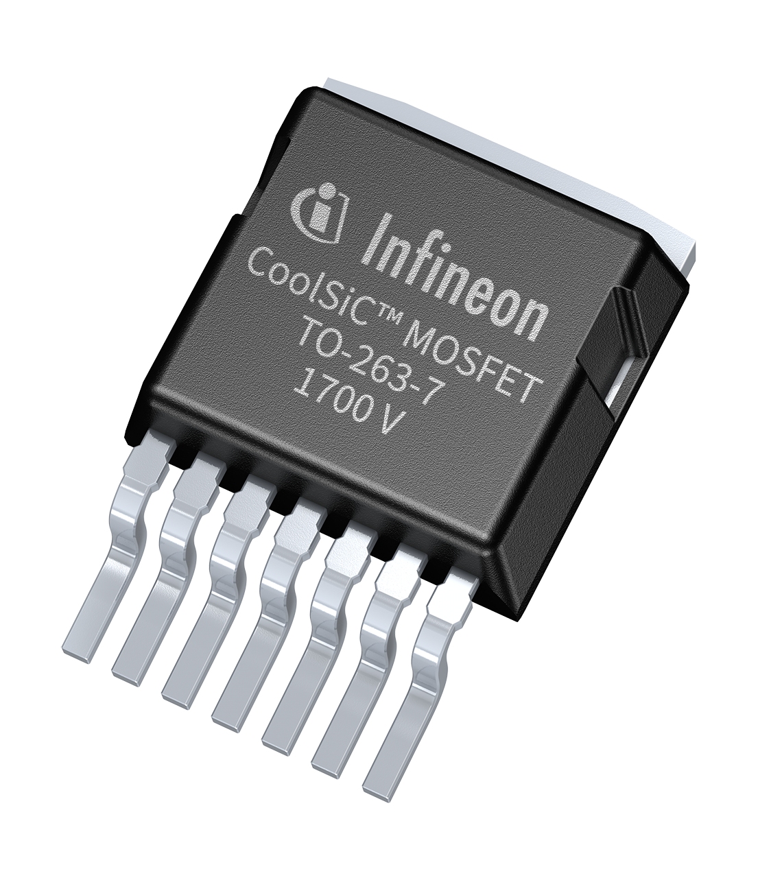
Infineon’s CoolSiC™ MOSFETs use an optimized, state-of-the-art trench semiconductor process that enables both the lowest losses in the application and the highest reliability in operation. The products, with voltage classes of 1700 V, 1200 V, and 650 V and forward resistances from 27 mΩ up to 1000 mΩ, are ideally suited for integration in applications such as photovoltaic inverters, battery charging, energy storage, motor drives, UPS, auxiliary power supplies and SMPS ab. Infineon’s CoolSiC MOSFETs are available at www.rutronik24.com.
The MOSFETs in discrete packages are ideal for power factor correction (PFC) circuits, bidirectional topologies, and DC-DC converters or DC-AC inverters. They also impress with excellent immunity to unwanted parasitic turn-on effects and low dynamic losses, even at zero volt turn-off voltage in bridge topologies.
Using CoolSiC™ Trench technology, a flexible parameter set is enabled, which is used to implement application-specific features in the respective product portfolio:
The 650 V CoolSiC™ MOSFETs, for example, offer optimized switching behavior at high currents and low capacitances. They are designed for industrial applications such as servers, telecommunications, and motor drives.
The 1200 V MOSFET range is suitable for both industrial and automotive applications such as on-board chargers/PFC, auxiliary inverters, and uninterruptible power supplies (UPS).
The flyback typology characterizes the 1700V variant, which makes it ideal for use in energy storage systems, fast charging of electric vehicles, power management (SMPS), and solar energy system solutions.
Less offers more Infineon’s EiceDRIVER™ offers a range of selected driver ICs that meet the requirements of extremely fast SiC MOSFET switching. Combined, the CoolSiC products enable improved efficiency, reduced cooling requirements, space and weight savings, part count reduction, and increased system reliability with a longer lifetime at lower system cost.
Features
Low component capacitances
Temperature-independent switching and low conduction losses, especially under part-load conditions
Intrinsic diode with low reverse recovery charge
Threshold-free on-state characteristics; threshold voltage Vth > 4 V
Excellent gate oxide reliability
IGBT compatible drive (+18 V)
Short circuit and avalanche robustness
Higher frequency operation
For more information about Infineon’s CoolSiC™ MOSFETs and a direct ordering option, please visit our e-commerce platform at www.rutronik24.com