MORNSUN has introduced two new drivers SCM1201BTA and SCM1212BTA that feature integrated MOSFETs for the primary side of a push-pull power and can be used in the 1-2W applications with 3.3V and 5V inputs. These new series with wide input voltage range of 2.7-5.5V will not be damaged even under the high input voltage up to 9V within 1s.
These devices contain, two drive systems and two power MOSFETs that are highly symmetrical and reduce the degree of magnetic bias in the push-pull topology. Moreover, these drivers are integrated with three key technologies to improve reliability meet the AEC-Q100 automobile standard to ensure reliability.
Key Features
Push-Pull driver controller
2.7-5.5V wide input voltage
Low conduction resistance 200mΩ
Two built-in power MOSFETs with high symmetry, quasi-complementary driver
Limited MOSFET’s current while turning on the power
Over current protection and short circuit protection
Over temperature protection
Under voltage protection
Increase the dead time under light load
Meet AEC-Q100 automobile standard
Application Diagram
These devices can be widely used in isolated power supply, industrial process control, isolated communication power supply, medical device, telecommunication equipment, etc.
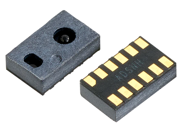
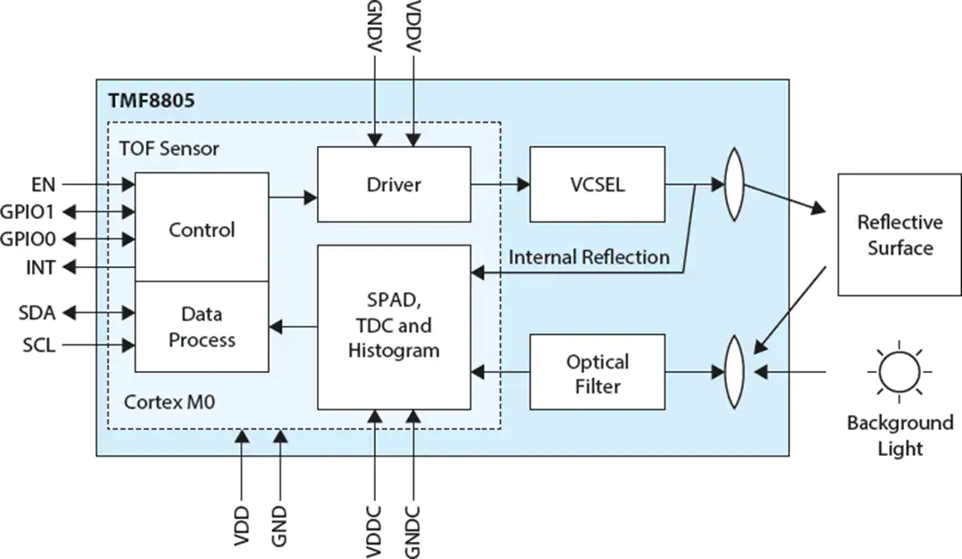
The TMF8805 is a true direct time-of-flight sensor and processing system in a highly integrated modular package. It integrates a 940nm Class 1 eye-safe VCSEL, a high-sensitivity SPAD array, precision time-to-digital converter and a low-power microcontroller sub-system.
The embedded histogram algorithm can detect cover glass and objects behind glass, selecting the object with highest SNR while compensating for dirt and smudges on cover glass. This device is ideally suited to world-facing camera LDAF applications, user presence detection, collision avoidance, object detection and other applications in the range of 2 to 250cm.
Features
20mm to 2500mm distance sensing at 30Hz
Direct ToF technology with high sensitivity SPAD detection
Delivers high SNR, wide dynamic range, and no multi-path reflections
Enables dark and sunlight environment distance measurement within ±5%
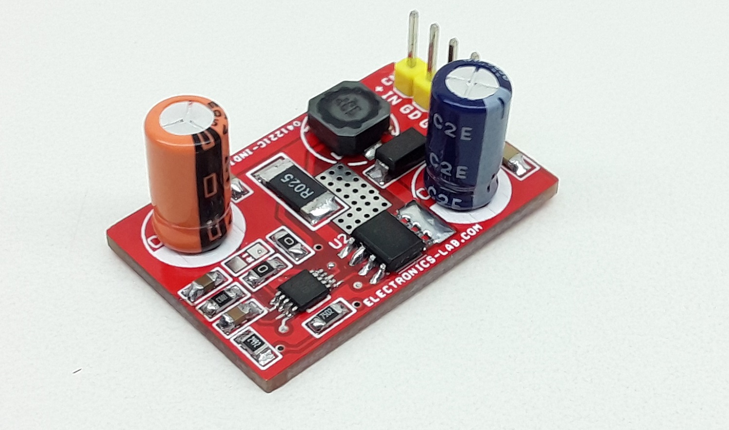
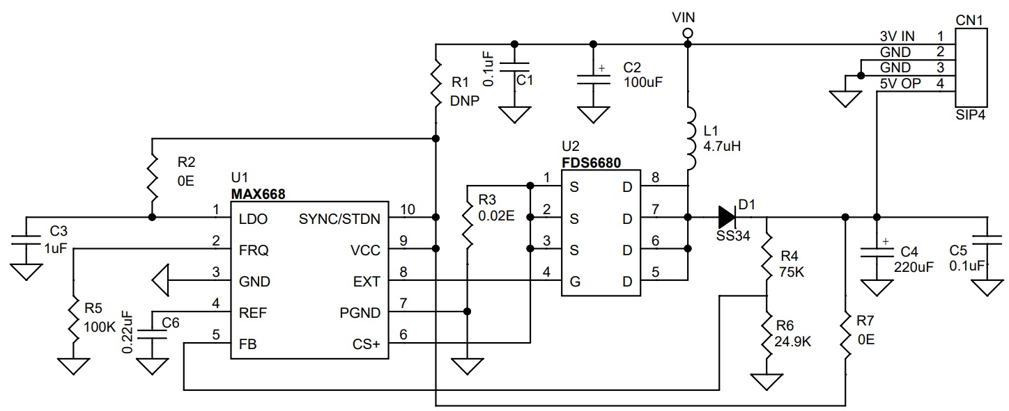
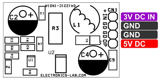
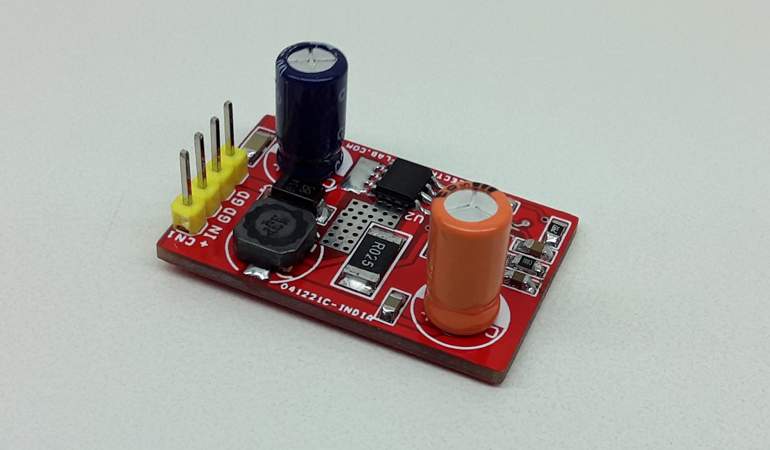
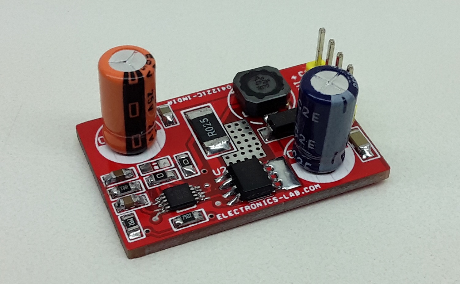
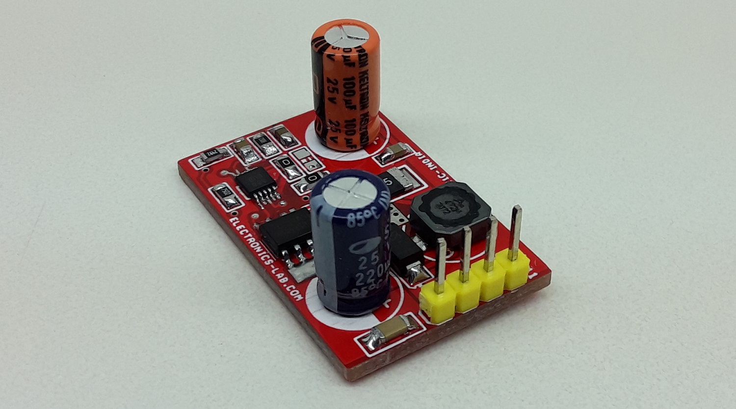
The project presented here is a powerful constant-frequency, pulse-width modulating (PWM), current-mode step-up DC-DC switching regulator efficiently producing 5V from input voltages between 3V to 5V. The project can be used in a portable device that works with a battery. The module produces a peak current of up to 1A and an output voltage of 5V DC.
The MAX668 current-mode PWM controllers operate in a wide range of DC-DC conversion applications, including boost, SEPIC, flyback, and isolated output configurations. Optimum conversion efficiency is maintained over a wide range of loads by employing both PWM operation and Maxim’s proprietary Idle Mode control to minimize operating current at light loads. Other features include shutdown, adjustable internal operating frequency or synchronization to an external clock, soft start, adjustable current limit, and a wide (1.8V to 28V) input range.
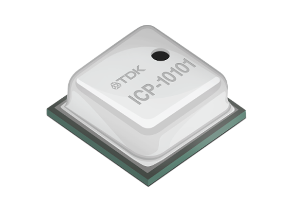
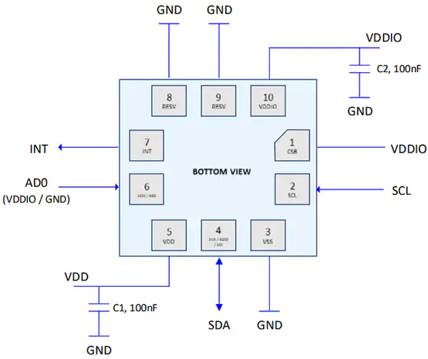
TDK InvenSense SmartPressure™ Barometric Pressure Sensor is a high-accuracy, low power, barometric pressure, and temperature sensor solution. This ICP-20100 module integrates a capacitive pressure sensor for monitoring pressure changes in the range of 30kPa to 110kPa. The sensor also has a DSP module for on-chip calibration with an analog-to-digital converter (ADC), digital filtering, a FIFO, and has I2C, I3CSM, and SPI interfaces available. The ICP-20100 can be configured to achieve ultra-low noise or ultra-low power performance and is flexible to perform anywhere in-between. TDK InvenSense SmartPressure Barometric Pressure Sensor is available in a closed 2mm x 2mm x 0.8mm 10-pin LGA package with a vent hole. Applications include smartphones and tablets, wearable Sensors, drones and toys, fitness trackers, home and building automation, and weather stations.
Features
Digital-output pressure and temperature sensors, with programmable output – all pressure, all temperature, or pressure and temperature
Programmable noise performance down to 0.5Parms through programmable oversampling ratio (OSR)
96-byte FIFO buffer enables the application processor to read up to 16 pressure-temperature pairs in a burst
Digital filtering for pressure signals
Finite impulse response (FIR) filter for improved noise performance
Infinite impulse response (IIR) filter for filtering of pressure glitches
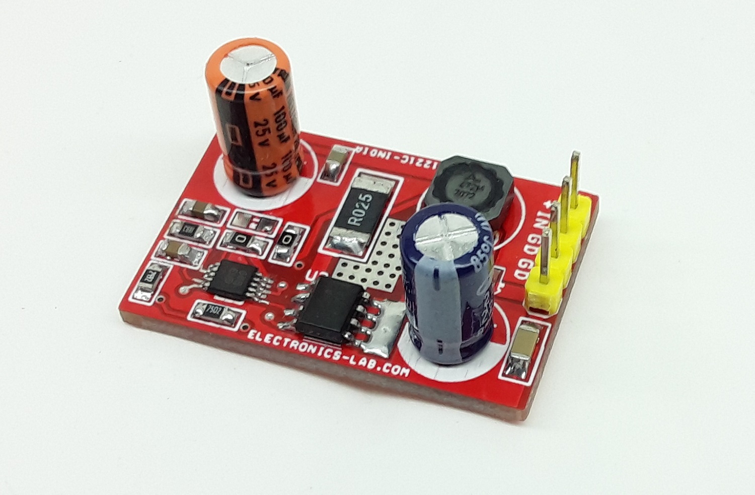
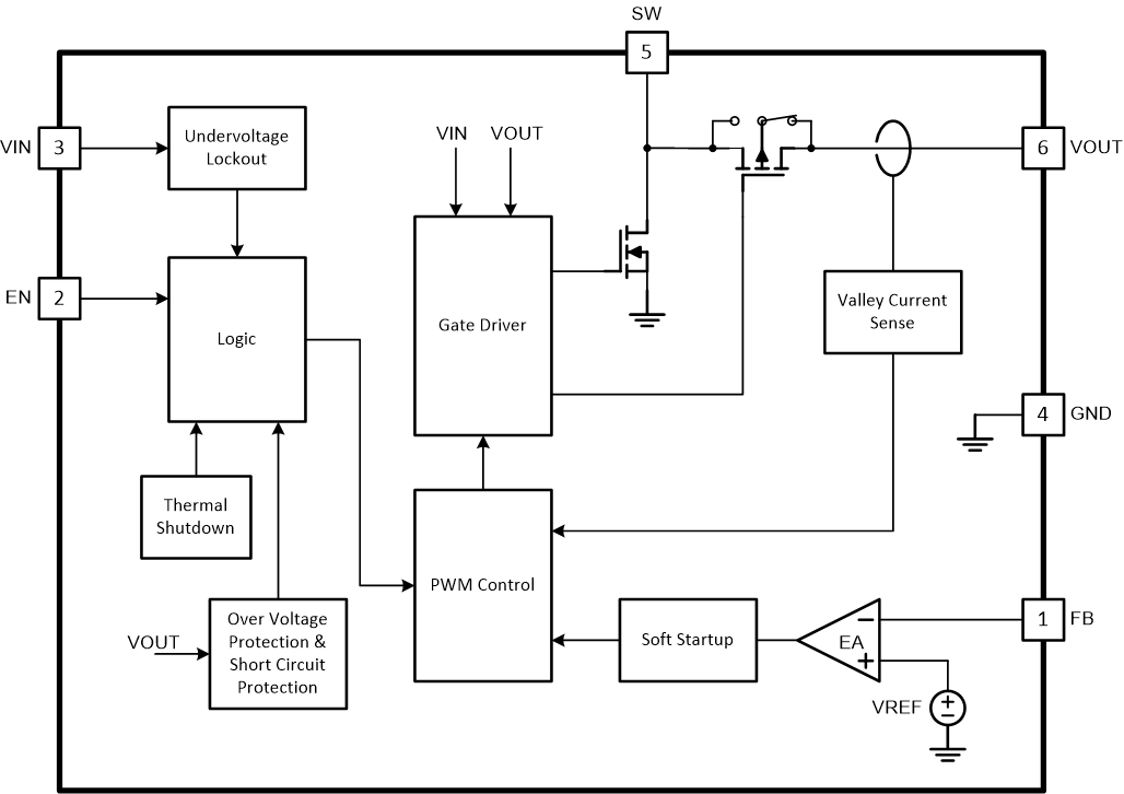
TPS61023 device is a synchronous boost converter with 0.5-V ultra-low input voltage. The device provides a power supply solution for portable equipment and smart devices powered by various batteries and super capacitors. The TPS61023 has typical 3.7-A valley switch current limit over full temperature range. With a wide input voltage range of 0.5 V to 5.5 V, the TPS61023 supports super capacitor backup power applications, which may deeply discharge the super capacitor.
The TPS61023 operates at 1-MHz switching frequency when the input voltage is above 1.5 V. The switching frequency decreases gradually to 0.5 MHz when the input voltage is below 1.5 V down to 1 V. The TPS61023 enters power-save mode at light load condition to maintain high efficiency over the entire load current range. The TPS61023 consumes a 20-µA quiescent current from VOUT in light load condition. During shutdown, the TPS61023 is completely disconnected from the input power and only consumes a 0.1-µA current to achieve long battery life. The TPS61023 has 5.7-V output overvoltage protection, output short circuit protection, and thermal shutdown protection.
The TPS61023 offers a very small solution size with 1.2-mm×1.6-mm SOT563 (DRL) package and minimum amount of external components.
Features
Input voltage range: 0.5V to 5.5V
1.8V Minimum input voltage for start-up
Output voltage setting range: 2.2V to 5.5V
Two 47mΩ (LS) / 68mΩ (HS) MOSFETs
3.7A Valley switching current limit
94% Efficiency at VIN = 3.6V, VOUT = 5V and IOUT = 1.5A
1MHz Switching frequency when VIN > 1.5V and 0.5MHz switching frequency when VIN < 1V
Typical 0.1µA shutdown current from VIN and SW
±2.5% Reference voltage accuracy over -40°C to +125°C
Auto PFM operation mode at light load
Pass-through mode when VIN > VOUT
True disconnection between input and output during shutdown
Output overvoltage and thermal shutdown protection
In the previous articles, we discussed that the digital logic uses Boolean data type which comprises of only two states i.e. “0” and “1”, and which are also referred to as “LOW” and “HIGH” states, respectively. The set of rules and laws can be applied to Boolean data types to find the optimum solution. As such, a digital logic circuit can be expressed in a Boolean Algebraic equation, and, by applying Boolean rules, laws, and theorems on this equation, an optimum digital circuit can be deduced. This optimum digital circuit benefits reduced logic, size, power consumption, and cost. Augustus DeMorgan, an English Mathematician, gave two famous laws known as DeMorgan’s Theorems which imparted a major contribution to Boolean Algebra. DeMorgan’s Theorems will be explained later in this article. However, in simple words, DeMorgan’s Theorems can be used to find the equivalency of NAND and NOR gates by viewing these operations as separate NOT-AND and NOT-OR functions, respectively.
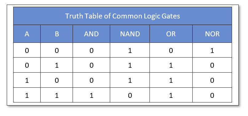
The truth table comprising of AND, NAND, OR, and NOR logic functions against two inputs is given below. These logical functions are used in DeMorgan’s Theorems and, as such, given to recall these logical operations.
The above given logical functions are denoted by equivalent Boolean notations. A “.” between operands means AND (Multiplication) operation, a “+” means OR (Sum) operation, and overline means an inversion of the operand. The equivalent Boolean notations of commonly used logical functions are shown in the following table.
DeMorgan’s Theory
DeMorgan’s Theory states two sets of laws or rules which are applicable to Boolean expressions having AND, OR, and NOT logical operations with two inputs (or more). Using these theorems, the logical operation of two variables is negated and converted into another logical operation. Such as, the logical NOR operation on two (or more) variables is equivalent to inversion of these variables and AND’ed together. Similarly, the logical NAND operation on two (or more) variables is equivalent to inversion of these variables and OR’ed, together. In other words, using DeMorgan’s theorems, the AND operator is replaced with the OR operator, and the OR operator is replaced with the AND operator.
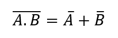
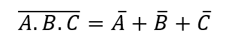
DeMorgan’s First Theorem
According to DeMorgan’s First Theorem, the resultant of two (or more) variables AND’ed and inverted (NOT) as a whole is equivalent to the OR of the complements of individual variables. Thus, AND + NOT (NAND) operation on variables is equivalent to the sum (OR) of the individual complement of each variable. In Boolean expression, it is stated as follow:
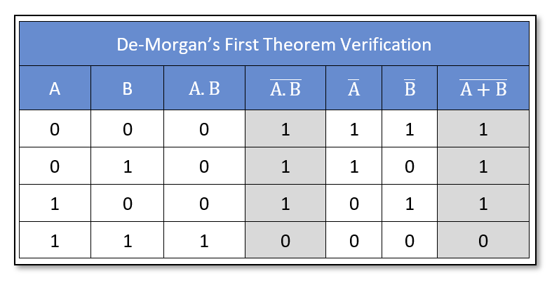
Verification of DeMorgan’s First Theorem using Truth Table
DeMorgan’s First Theorem can be verified using a truth table as illustrated below:
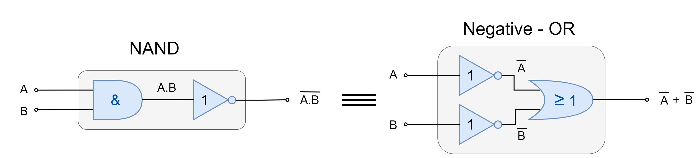
DeMorgan’s First Law Implementation
The following figure shows the implementation of DeMorgan’s First Theorem. The two logic circuits are equivalent to each other as per DeMorgan’s First Theorem.
Figure 1: Implementation of DeMorgan’s First Theorem
The left logic circuit forms a NAND (AND + NOT) gate. Whereas the right logic circuit, first inverts the inputs then they are OR’ed. These two logic circuits are equivalent to each other i.e. NAND = negative-OR. It can also be stated that a complement can be shifted from the output of the AND gate to the individual input of an OR gate and will be identical in logic operation as per the first theorem of DeMorgan.
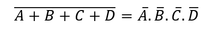
DeMorgan’s Second Theorem
According to DeMorgan’s Second Theorem, the resultant of two (or more) variables OR’ed and inverted (NOT) as a whole is equivalent to the AND of the complements of individual variables. Thus, OR + NOT (NOR) operation on variables is equivalent to AND of the individual complement of each variable. In Boolean expression, it is stated as follow:
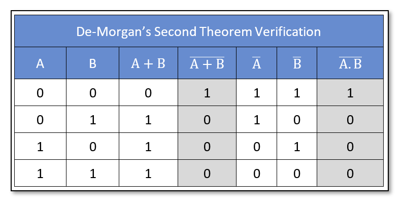
Verification of DeMorgan’s Second Theorem using Truth Table
DeMorgan’s Second Theorem can be verified using a truth table as illustrated below:
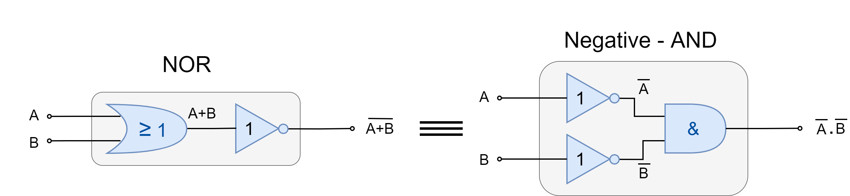
DeMorgan’s Second Law Implementation
The following figure shows an implementation of DeMorgan’s Second Theorem. The two logic circuits are equivalent to each other as per DeMorgan’s Second Theorem.
Figure 2: Implementation of DeMorgan’s SecondTheorem
The left logic circuit forms a NOR (OR + NOT) gate. Whereas the right logic circuit, first inverts the inputs then they are AND’ed. These two logic circuits are equivalent to each other i.e. NOR = negative-AND. It can also be stated that a complement can be shifted from the output of OR gate to individual input of an AND gate and will be identical in logic operation as per the second theorem of DeMorgan.
Thus, according to DeMorgan, an AND operation on inverted inputs is equivalent to NOR (OR + NOT) operation and vice versa. Similarly, an OR operation on inverted inputs is equivalent to NAND (AND + NOT) operation and vice versa.
In the above text, DeMorgan’s theorems have been applied to two-input variables. However, theorems are equally valid for more than two inputs variables.
For three-input variables:
DeMorgan’s First Theorem:
DeMorgan’s Second Theorem:
For four-input variables:
DeMorgan’s First Theorem:
DeMorgan’s Second Theorem:
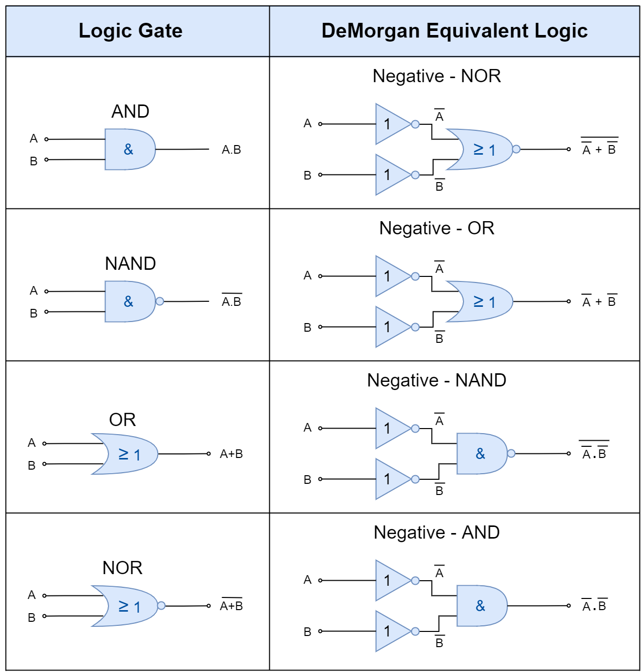
DeMorgan’s Equivalent Gates
The standard logic gates i.e. AND, NAND, OR, and NOR representing DeMorgan’s theorems can be obtained. It has already been discussed above that the NAND (AND + NOT) operation can be replaced by the OR logic on inverted inputs. Here, firstly, AND logic is replaced with the OR, and, secondly, the inversion is applied at the inputs and outputs. Resultantly, the AND + NOT logic becomes NOT + OR. The inputs which were originally not inverted become inverted and inverted output becomes non-inverted. The same can be applied to DeMorgan’s Second Theorem to obtain equivalent logic gates.
The following table shows the standard equivalent logic gates of DeMorgan’s theorems.
Conclusion
Augustus DeMorgan, an English Mathematician, gave two famous laws known as DeMorgan’s Theorems which are used to find the equivalency of the NAND and NOR logic gates.
DeMorgan’s First Theorem states that the NAND gate can be replaced with the OR function having inverted inputs i.e. Invert-OR logic.
DeMorgan’s Second Theorem states that the NOR gate can be replaced with the AND function having inverted inputs i.e. Invert-AND logic.
According to DeMorgan’s theorems, the AND logic can be replaced with the OR logic with inversion applied at the inputs and the output. Similarly, the OR logic can be replaced with the AND logic with inversion applied at the inputs and the output.
The AND logic can be replaced with the Inversion-NOR logic.
The NAND logic can be replaced with the Inversion-OR logic.
The OR logic can be replaced with the Inversion-NAND logic.
The NOR logic can be replaced with the Inversion-AND logic.
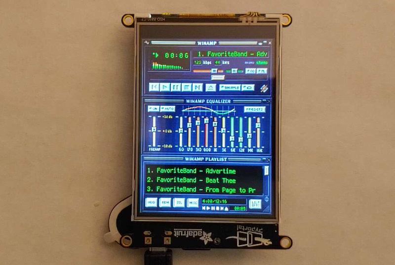
This project will turn your PyPortal into an MP3 player to play your favorite tunes with the familiar Winamp look. Create and manage multiple JSON playlists and rock out to whichever one fits the mood.
Take it a step further by choosing a custom Winamp skin and converting it for use on your PyPortal.
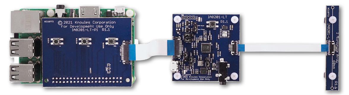
The Knowles AISonic audio edge processor IA8201 is a high-performance, ultra-low-power audio-centric OpenDSP supporting up to 4 mics, multiple high-speed interfaces, and GPIOs in two package options (eWLB and QFN). It provides low power, high efficiency, privacy, and compute power enabling customers to design modern products with far-field voice processing functionality for accurate listening. The IA8201 enables wake-on-voice processing for low latency voice UI, noise reduction, context awareness, and accelerated machine learning inferencing for edge processing of sensor inputs.
Knowles currently utilizes a modular approach to add voice with the capability to work with existing platforms and MCUs. IA8201 allows easy integration with legacy MCU system boards by running these commands over a simple UART interface.
The IA8201-RDI-01 is an evaluation kit based on the Knowles AISonic audio edge processor IA8201. It is a complete system-level solution that enables Knowles customers to quickly go from an idea to a front-end audio solution that meets their platform requirements. It includes an IA8201-LT dev board, Raspberry Pi connector board, one 3-mic array, one 2-mic array, and flex cable connectors. The system firmware release to connect this platform is available on solution.knowles.com. It also comes with support of Sensory Voice Hub, which allows a user to create wake-words and local commands using a Web-based voice user interface.
Use Case Examples
Low power voice wake: Listens for specific OEM keywords to wake the host processor. Large memory enables processing of multiple stages on-chip for accurate results.
Proximity detection: When combined with an ultrasonic capable speaker and microphone, detects the distance between the system and an object; can replace an IR-Prox sensor in bezel-less phones.
Hub: Determines location of voice source while tuning out a noisy environment and lowering music to detect voice commands. Simultaneously takes metadata input and overrides beamformer to focus on camera-tracked objects.
Security system: Activate with a voice command. Detect glass breakage/smoke alarm, log direction of noise source, trigger alarm, and send alerts through Wi-Fi connection.
Wireless earbuds: Delivers low power premium wake-on-voice performance, talk detection to eliminate false triggers, enhanced voice quality through advanced beamforming and noise reduction algorithms, and support for local commands, including answer/ignore calls.
Features
Multi-Core: DeltaMax, optimized for compute; HemiDelta, optimized for low power
Audio interfaces: Up to 4x PDM digital microphones – 1 stereo inputs, 4 x mono inputs, and 1 stereo output, supporting clock rates up to 6.144 MHz; up to 3x PS/TDM ports supporting 8 channels each of 32-bit audio data using a 24.576 MHz input clock
Control interfaces: SPI, I2C, UART, available GPIOs
Memory: 1.44 MB RAM (1 MB available to users)
Clock: 175 MHz
Packaging options: eWLB 3.00 mm x 2.6 mm x 0.715 mm, 0.4 pitch, 42 ball; QFN 6.00 mm x 6.00 mm x 0.75 mm, 0.5 pitch, 40 lead
System requirements: IA8201BC 1.8 VDD, IA8201CQ 1.8 VDD and 3.3 VDD, -20°C to +85°C
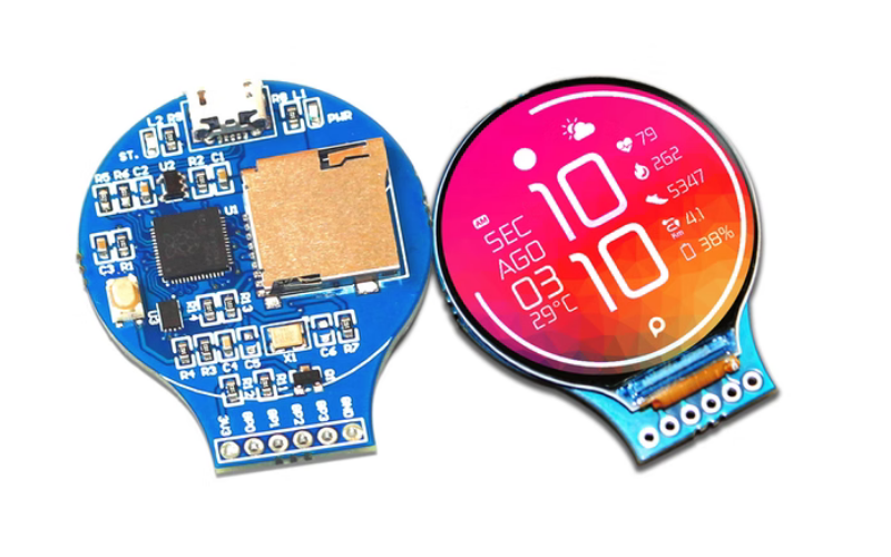
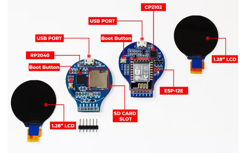
UK-based hardware developer Om Singh has launched a crowdfunding project built on two popular microcontrollers, RP2040 and ESP32. The RoundyPi, as the name suggests, is a Raspberry Pi’s in-house silicon tape-out RP2040 powered, compact and stylish LCD display of size 1.28-inches. RP2040 brings its distinctive characteristics of high performance, low cost, and ease of use to the microcontroller space. With a display of a 1.28-inch color screen and a resolution of 240×240 pixels, as well as an SD card slot, USB port, and the GC9A01 driver, bring down the number of I/O pins required. RoundyPi features two USB ports, one for power transmission and the other for data transmission, and provides one slot for an SD card.
The high-performance MCU RP2040 is quite flexible and versatile with digital screens that deliver remarkable efficiency and power for petite and compact dimensions. It incorporates a minimal-power ARM dual-core Cortex-M0+ processor with a CPU speed of up to 133MHz. Furthermore, the RP2040 features 264KB on-chip RAM, a DMA controller, two UARTs, two SPI controllers, and two I2C controllers, which together enable the module to run efficiently and quickly. Among the most appealing features of this low-cost microcontroller is the incorporation of a potentially powerful chip, the RP2040, at an unbeatable price, which will help clients construct cost-effective embedded electronics components or projects.
Another product, RoundyFi, based on the ESP-12E is a circular LCD with an elegant and sleek display unit of the same size as RoundyPi of 1.28 inches with 240×240 resolution and 65K RGB colors. It offers a vivid and vibrant effect that will enhance and boost the project’s user interface. Featuring an inbuilt GC9A01 driver and an SPI interface, RoundyFi considerably reduces the number of I/O pins required. Circular-shaped LCD displays have gotten trendy recently as they offer the project a modest and impressive appeal, which is often quite aesthetically pleasing.
Wireless power network provider, Energous Corporation, has revealed its association with Syntiant, to develop Energous’ WattUp wireless power network technology with Syntiant’s Neural Decision Processors (NDPs) for edge artificial intelligence deployments across a wide range of consumer and industrial use cases.
Syntiant, the California-based tech company, integrates the “most efficient silicon with a data platform and a training pipeline”, thereby furnishing its users with low-cost and turn-key solutions that embed deep learning processing in almost any edge device, ensuring privacy and security while avoiding cloud connectivity. From earbuds, medical gadgets, smart home appliances to industrial IoT equipment, and vehicles all avail the usage of Syntiant’s ultra-low-power NDPs. Syntiant’s AI processors furnish 100x more performance and 10x the throughput relative to current reduced power microcontroller unit solutions, owing to a clean-sheet, hardware/software co-design approach.
“Syntiant’s Neural Decision Processors help reduce infrastructure costs by moving AI processing from the cloud to the edge, reliably, securely and with nominal power consumption”, said CEO of Syntiant, Kurt Busch.
“We share a similar perspective with Energous that much of tomorrow’s innovation is happening at the edge, and our collaboration will successfully demonstrate both technologies working together, delivering power where it is not while providing highly accurate, cloud-free inference across a wide range of consumer and industrial applications.”
Energous includes a WattUp PewerBridge transmitter that discharges conducted radio frequency power in a determined arena or direction, unlike passive solutions that garner energy from the neighboring environment, which tends to offer incredibly low amounts of power and can be inherently uncertain about how much power is accessible. The receiving devices, then gather this RF-based energy. Extending improvements in power, efficiency, foreign device detection, freedom of movement, and the overall cost is the main aim behind the positioning of WattUp. It is built on fast, efficient, and highly scalable RF-based charging technology.
Energous wireless power networks provide “one to many” charging, which means that a single transmitter can charge numerous devices at the same time. It can be used in a variety of industries and applications, including medical, storage, monitors, and patient trackers in healthcare, smoke detectors and motion sensors in smart homes, and defect prevention, temperature, and other safety sensors in industrial settings.