Rohde & Schwarz presents R&S RT-ZISO isolated probing system for precise measurements of fast switching signals

Rohde & Schwarz has developed the R&S RT-ZISO isolated probing system, further elevating its cutting-edge oscilloscope portfolio. The new R&S RT-ZISO enables extremely accurate measurements of fast switching signals, especially in environments with high common-mode voltages and currents. Also new is the R&S RT-ZPMMCX passive probe with MMCX connector, which complements the isolated probe system perfectly for certain measurement tasks.

At the PCIM Europe International Exhibition and Conference in Nuremberg, Germany, Rohde & Schwarz is giving a sneak peek at its next generation R&S RT-ZISO isolated probing system. The R&S RT-ZISO will set new standards in isolated probe technology, delivering unprecedented accuracy, sensitivity, dynamic range, and bandwidth for next generation wide bandgap (WBG) power designs with SiC and GaN.

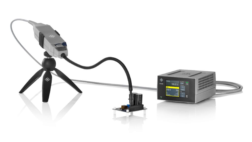
The R&S RT-ZISO provides precise differential measurements of up to ±3 kV on reference voltages of ±60 kV with a rise time of < 450 ps and suppresses fast common-mode signals that can distort and interfere with accurate measurements. Its power-over-fiber architecture galvanically isolates the device under test (DUT) from the measurement setup, providing a much higher common-mode rejection ratio (CMRR) than conventional differential probes. Its key features include bandwidth options of 100 MHz to 1 GHz (upgradeable), a CMRR of > 90 dB (> 30 000:1) at 1 GHz, an input and offset range of ±3 kV, a common mode range of ±60 kV, and a sensitive input range of ±10 mV.

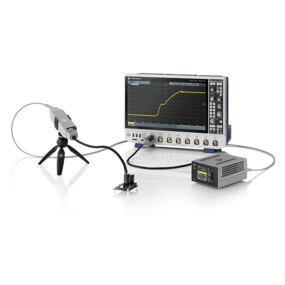
The R&S RT-ZISO isolated probe is the perfect addition to the Rohde & Schwarz oscilloscope portfolio. With the instruments of the next generation MXO series (MXO 4, MXO 5, MXO 5C), the probe enables measurements with the world’s fastest acquisition in the time and spectrum domain, thanks to the oscilloscopes’ hardware-based acceleration. In combination with the R&S RTO6, design engineers can use the probe for complex analysis tasks that take advantage of the oscilloscope’s high performance and advanced measurement capabilities.

The R&S RT-ZISO is ideal for a wide range of applications, including switching analysis of power converters with WBG materials, double-pulse testing, floating measurements, shunt measurements, inverter design, and motor drive analysis. The isolated probing system comes with a range of probe tips for different measurement needs, including the micro-miniature coaxial (MMCX) connector, square pins, wide square pins and the isolated passive prober. All connectors are rated for CAT III voltages up to 1000 V. It is the first passive isolated prober on the market that allows users to quickly access the test point without designated connectors. In addition, the use of long bandable cables allows the tips to access the DUT at various angles with no additional mechanical stress.

R&S RT-ZPMMCX passive probe with MMCX connector

Along with the R&S RT-ZISO, Rohde & Schwarz is also presenting a new type of passive probe with MMCX connector. The R&S RT-ZPMMCX supports a bandwidth range of > 700 MHz with input voltages of ±60 V DC and 30 V (RMS), making it the ideal complement to the R&S RT-ZISO isolated probing system for low-side gate measurements. The MMCX probe has a very low capacitive load of < 4 pF, which helps to maintain the best signal integrity for preserving the switching waveform shape and timing.

The R&S RT-ZISO isolated probing system and the R&S RT-ZPMMCX passive probe are both available from Rohde & Schwarz. Visitors to the PCIM Europe International Exhibition and Conference, June 11 to 13, 2024, in Nuremberg, Germany, can experience them live at the company’s booth 619 in hall 7.

For more information on the R&S RT-ZISO isolated probing system,visit: https://www.rohde-schwarz.com/_334271.html.

For an overview of all oscilloscope probes from Rohde & Schwarz, visit: https://www.rohde-schwarz.com/_229530.html

Half Bridge with Single PWM Input

This is a Half-bridge module based on the LM5104 chip, which is a high-voltage gate driver. This High-Voltage Gate Driver is designed to drive both the high-side and the low-side N-channel MOSFETs in a synchronous buck configuration. The floating high-side driver can work with supply voltages up to 100V. The high-side and low-side gate drivers are controlled from a single PWM input. Each state change is controlled adaptively to prevent shoot-through issues. In addition to the adaptive transition timing, an additional delay time can be added, proportional to an external setting resistor. An integrated high-voltage diode is provided to charge the high-side gate drive bootstrap capacitor. A robust level shifter operates at high speed while consuming low power and providing clean level transitions from the control logic to the high-side gate driver. Undervoltage lockout is provided on both the low-side and the high-side power rails.

The user must take care of the following:

  • Bootstrap capacitor value depends on the input frequency
  • Choose the right MOSFET as per Load Current/Voltage
  • Choose the Right Value for delay resistor R4-RT, Depending on MOSFET Gate Capacitance. Refer to Datasheet for more info.

Features

  • Power Supply Load up to 48V (Limited Due to Capacitor Volt)
  • Power Supply Gate Driver 9V to 14V DC
  • Load Up to 5Amps (Higher with Cooling Fan)
  • Drives Both a High-Side and Low-Side N-Channel MOSFET
  • Adaptive Rising and Falling Edges with Programmable
  • Additional Delay
  • Under Voltage Threshold 7V
  • Adjustable Delay 90 to 200nS (RT(R4) 10K to 100K)
  • Operating Frequency Input up to 1000Khz
  • Single Input Control
  • Bootstrap Supply Voltage Range up to 118-V DC
  • Fast Turnoff Propagation Delay (25 ns Typical)
  • Drives 1000-pF Loads With 15-ns Rise and Fall Times
  • Supply Rail Under Voltage Lockout
  • On Board Power LED
  • Screw Terminals for Load Supply and Load
  • Header Connector for Input signal and Gate Driver Supply
  • 5mm x 4 PCB Mounting Holes
  • PCB Dimensions 44.45 x 29.53 mm

Applications

  • Current Fed Push-Pull Power Converters
  • High Voltage Buck Regulators
  • Active Clamp Forward Power Converters
  • Half-Bridge and Full-Bridge Converters

Connections

  • CN1: Pin 1 Power Supply Load 48V DC, Pin 2 = GND
  • CN2: Pin 1 Output, Pin 2 = GND
  • CN3: Pin 1 VDD 9V to 14V, Pin 2 = Load Power Supply, Pin 3 = PWM Input, Pin 4 = GND
  • D1: Power LED

Schematic

Parts List

NOQNTY.REF.DESC,MANUFACTURERSUPPLIERSUPPLIER PART NO
12CN1,CN22 PIN SCREW TERMINAL PITCH 5.08MMPHOENIXDIGIKEY277-1247-ND
21CN3 4 PIN MALE HEADER PITCH 2.54MMWURTHDIGIKEY732-5317-ND
31C1100nF/50V CERAMIC SMD SIZE 0805YAGEO/MURATADIGIKEY
41C2220uF/50V ELECKTROLYTICPANASONICDIGIKEYPCE3921CT-ND
51C3100nF/50V CERAMIC SMD SIZE 0805YAGEO/MURATADIGIKEY
61C447uF/35V ELEKTROLYTICWURTHDIGIKEY732-8508-1-ND
71C5100nF/50V CERAMIC SMD SIZE 0805YAGEO/MURATADIGIKEY
81D1LED SMD SIZE 0805OSRAMDIGIKEY475-1278-1-ND
92D2,D31N4148ONSEMIDIGIKEYFDLL4148CT-ND
102Q1,Q2FDD86369 DPAKONSEMIDIGIKEYFDD86369OSCT-ND
111R12.2K 5% SMD SIZE 0805YAGEO/MURATADIGIKEY
122R2,R310E 5% SMD SIZE 0805YAGEO/MURATADIGIKEY
131R447K 5% SMD SIZE 0805YAGEO/MURATADIGIKEY
141U1LM5104 SOIC8TIDIGIKEYLM5104MX/NOPBCT-ND

Block Diagram

Connections

Typical Application

Gerber View

Photos

Video

LM5104 Datasheet

Self-Oscillating Half Bridge Module

This is an automotive-grade self-oscillation 50% duty cycle half-bridge module built using the AUIR2085S chip from Infineon. The project consists of 2 x N-channel MOSFETs, and the module provides a primary side control solution to enable Half-Bridge DC-bus converters. The module is a self-oscillating half-bridge driver with 50% duty cycle ideally suited for 10V – 15V half-bridge DC-bus converters.   The board is also suitable for push-pull converters. Each channel frequency is equal to fOSC, which can be set by selecting RT (R2+PR1) & CT-(C7), Dead-time can be controlled through proper selection of CT range from 50ns to 200ns. Internal soft-start increases the pulse width during power-up and maintains pulse width matching for the high and low outputs throughout the start-up cycle. Typically, the soft-start duty cycle varies beginning from 5-10% ramping up to about 50% over 1000 cycles.  The AUIR2085S initiates a soft start at power up and after every overcurrent condition. Undervoltage lockout prevents operation if VCC is less than 7.5V.

Features

  • Power Supply 10V to 14V DC
  • Integrated 50% duty cycle oscillator and half-bridge driver
  • Adjustable switching frequency 84Khz to 260Khz
  • Undervoltage lockout prevents operation if VCC is less than 7.5V.
  • +/- 1A drive current capability optimized for low-charge MOSFETs
  • Adjustable dead-time 50ns – 200ns (Read Data Sheet for More Info)
  • High and low side pulse width matching to +/- 25ns
  • Adjustable overcurrent protection (Shunt Resistor Value)
  • Over Current Shut Down Threshold 300mV
  • Over Current Shutdown Delay 200nS
  • Turn-on Rise Time 40nS
  • Turn-off Fall Time 20nS
  • Undervoltage lockout and internal soft start
  • PCB Dimensions 40.16 x 21.27 mm

Push-Pull Converter Application

The components like transistors Q1, Q2, the external transformer, and the capacitors C4, C5, C9, and C10 make up a so-called single-ended, push-pull converter. This converter operates the potential-isolating transformer with an alternating voltage in which both half-oscillations are used for energy transmission.

Frequency Adjust

A Trimmer potentiometer is provided to adjust the frequency from 84Khz to 200Khz. The module supports higher frequencies up to 500Khz, read the datasheet of the AUIR2185S chip to learn more about frequency and dead time adjustment. For 500Khz Output CT should be 100pF and RT 10kΩ.

Applications

  • DC-DC Converters, Push-Pull Drivers
  • High Voltage Converters
  • HEV Auxiliary Converter
  • Battery Management Converters

The recommended range of timing resistors RT is between 10kΩ and 100kΩ and the range of timing capacitor CT is between 47pF and 470pF. Timing resistor values less than 10kΩ should be avoided. The value of the timing capacitor determines the amount of dead time between the two output drivers: the lower the CT, the shorter the dead time, and vice versa. It is not recommended to use a timing capacitor below 47pF, for best performance keep the timing components physically as close as possible to the AUIR2085S. Separated ground and VCC traces to the timing components are encouraged.

Connections

  • CN1: Pin 1 Output 2, Pin 2 Output 1 (for Push-Pull)
  • CN2: Pin 1 VCC, Pin 2 GND
  • PR1: Oscillator Adjust
  • D1: Power LED

Schematic

Parts List

NOQNTY.REF.DESC.MANUFACTURERSUPPLIER SUPPLIER PART NO
12CN1,CN22 PIN SCREW TERMINAL PITCH 5.08MMPHOENIXDIGIKEY277-1247-ND
21C147uF/25V CERAMIC SMD SIZE 1210MURATA/YAGEODIGIKEY
31C2220nF/25V CERAMIC SMD SIZE 1210 OR 1206MURATA/YAGEODIGIKEY
42C5,C104.7uF/25V CERAMIC SMD SIZE 1210 OR 1206MURATA/YAGEODIGIKEY
52C4,C9DNP
61C6100nF/100V CERAMIC SMD SIZE 1206MURATA/YAGEODIGIKEY
71C7100PF/50V CERAMIC SMD SIZE 0805MURATA/YAGEODIGIKEY
81C81nF/50V CERAMIC SMD SIZE 0805MURATA/YAGEODIGIKEY
91D1LED SMD SIZE 0805OSRAMDIGIKEY475-1278-1-ND
101D2SS34 OR SS14ONSEMIDIGIKEYSS34FSCT-ND
111PR150K TRIMMER POTBOURNSDIGIKEY3362P-503LF-ND
122Q1,Q2FDD8870 DPAKONSEMIDIGIKEYFDD8870FSCT-ND
131R12K 5% SMD SIZE 0805MURATA/YAGEODIGIKEY
141R222K 5% SMD SIZE 0805MURATA/YAGEODIGIKEY
152R3,R415E 5% SMD SIZE 0805MURATA/YAGEODIGIKEY
161R51K 5% SMD SIZE 0805MURATA/YAGEODIGIKEY
171R60.22E/2W 1% SMD SIZE 2512MURATA/YAGEODIGIKEY
181U1AUIR2085S SOIC8INFINEONDIGIKEYAUIR2085S-ND
191C34.7uF/25V CERAMIC SMD SIZE 0805MURATA/YAGEODIGIKEY

Connections

Block Diagram


Typical Application

Frequency Diagram

Gerber View

Photos

Video


AUIR2085S Datasheet

Camera Development board by LilyGo: T Camera+ S3

The addition of a camera module or developer board improves the device’s ability to record and interpret visual data, allowing for more advanced and diverse applications. With the rise in visual recognition techniques, the selection of camera modules becomes a crucial part also considering its compatibility with MCUs. Fulfilling these advanced requirements, the upcoming LILYGO has come up with a solution. The LILYGOs T-Camera-Plus-S3 ESP32-S3 Camera Development Board features a camera supporting resolution of up to 2 Million Pixels (IR-Cut Night Vision), a 1.3-inch capacitive touch display, a speaker [FUET2122], power supply cable and a Bluetooth/WI-FI antenna [3rd Generation].

Specifications of LILYGOs T-Camera-Plus-S3 ESP32-S3 Camera Development Board

It supports ESP32-S3R8 with a radio frequency of 2.4 GHz and becomes a versatile option for any IoT-based MCU. Dual-core Xtensa LX7 is the CPU of the ESP32-S3 chip. Xtensa is a line of CPUs designed by Intel specifically for low-power applications. LX7 refers to the specific CPU architecture within the Xtensa family.

Some of its key features:

  • Low Power Consumption
  • Integrated Wi-FI and Bluetooth
  • Support for Cameras
  • Frame Buffer Support: To facilitate quicker processing and manipulation, the ESP32-S3 may feature dedicated memory for storing image data taken by the camera.
  • Hardware Offloading: The chip has hardware accelerators designed specifically for image processing tasks thereby removing the processing burden of the CPU Cores.
  • Scalable Image Processing: It allows image manipulation tasks by leveraging hardware accelerators and adjusting processing based on complexity.
  • Serial Camera Control Interface (SCCI): It’s a simple serial interface which uses fewer pins. It is used for battery-powered applications with lower-resolution image capture.
  • Digital MIPI Camera Interface (DCAM): DCAM is a complex interface with multiple data lines. It is used for High resolution images or video captures.
  • Multiple Peripherals like SPI, I2C, GPIO, ADC, etc.

The camera operates at a voltage of 3.3V and it features a micro USB cable to interface it with any development boards. It showcases a reset button on board which is helpful during its testing phases and with the support of ESP32 it is easily programmed using popular platforms like Arduino IDE and Visual Studio Code.

Wireless Connectivity

The LILYGO Camera development board likely supports all three of those wireless technologies:

  • WI-FI 802.11: This allows the board to connect to the internet through a wireless router. This is useful for applications that need to send or receive data over the internet, such as streaming video from the camera or controlling the camera remotely.
  • BLE 5+ & Bluetooth Mesh: The BT Low Energy allows the users for short-range communication between devices whereas the BT Mesh Networking creates a network of BT devices that can communicate with each other such as a network of sensors for smart home automation.

Memory

The memory structure of T Camera Plus S3:

  • PSRAM (Pseudo Static RAM): The 8MB of PSRAM provides additional workspace for your application to run more complex algorithms or store temporary data while the camera is in use.
  • Flash: The 16MB of flash memory provides storage for the operating system, your application code, and any images or videos captured by the camera.
  • TF Card Slot: this enables storage of large amounts of image and video data captured by the camera during operation.

You can refer to the pin diagram for more details:


The Lilygo T-Camera-Plus-S3 development board has become a viable option for creating camera-based IoT prototypes. The combination of ESP32-S3 microcontroller, built-in camera capability, and a variety of wireless connectivity options enables developers to create a variety of applications ranging from smart surveillance systems to visual data analysis tools. The T-Camera-Plus-S3 provides a platform for rapid prototyping and development. Its compatibility with popular programming environments such as Arduino IDE and Visual Studio Code streamlines the development process. For more details, refer to the product page.

MYIR Tech Releases New MYC-J7A100T SoM and Dev Board

The MYC-J7A100T is a System-on-Module (SoM) designed by MYIR. It is based on the Xilinx Artix-7 XC7A100T FPGA chip, a field-programmable gate array that can be customized for various applications. FPGA is faster than regular Microcontrollers since they use parallel processing to execute multiple tasks at a time. This makes  MYC-J7A100T a high-density and high-speed circuit board.

Architectural Features of Xilinx Artix-7 XC7A100T FPGA chip:

  • Parallel execution of tasks.
  • Process Technology: 28 nm which allows higher performance & lower power consumption.
  • Logic Cells: 101,440
  • Configurable Logic Blocks (CLBs): 15,850
  • Flip-Flops: 126,800; implementing sequential logic.

It appears that the datasheet has more details one can refer to.

It features three types of onboard memory; The 512MB DDR3 memory(fastest) is used as the main memory for running applications. The 32MB QSPI FLASH (medium) is used for program storage and configuration settings. Meanwhile, the 32KB EEPROM (slowest) is utilized for storing data that requires infrequent updates, as well as user-specific data and configuration settings.

The SoM connects through a 260-pin MXM gold-finger-edge-card connector with a 0.5mm pitch. This connector is compatible with MYIR’s standard baseboard, which comes with the MYD-J7A100T development board. Additionally, it has 4 pairs of GTP high-speed transceiver interfaces and one JTAG interface. Notably, the GTP connections allow for high-speed communication with external devices, whereas the JTAG interface is crucial for development and debugging.

The SoM provides 178 configurable FPGA IOs to perform various functions depending on the user’s application.

These 178 IOs are divided into 4 banks as follows:

  • Operating Range is Fixed (3.3V)
    • Bank 13 with 35 IO pins
    • Bank 14 with 45 IO pins
  • Operating Range is user-configurable (1.2V~3.3V)
    • Bank 15 with 48 IO pins
    • Bank 16 with 50 IO pins


Bottom View of MYC-J7A100T

Development Board: MYD-J7A100T

The MYD-J7A100T is the development board that supports SoM MYC-J7A100T. It operates at a voltage of 5V/3A and works efficiently in temperatures ranging from -40 to 80 degrees celsius.

The development board MYD-J7A100T features:

Its expansion board

  • Interfacing with MYC-J7A100T SOM via a 0.5mm pitch 260-pin MXM gold-finger-edge-card connector socket.
  • 2 x Gigabit Ethernet ports.
  • 2 x SFP+ interfaces;

Used in networking for higher speed transmission over long ranges via fiber optics & copper connections.

  • 1 x PCIe 2.0 interface.
  • HDMI input and output interfaces.
  • 1 x DVP camera interface.
  • 1 x Micro SD slot.
  • 1 x USB-UART interface.
  • 1 x FAN interface.
  • 1 x 2.5mm pitch 2x 20-pin IO expansion interface.

Top View of MYD-J7A100T

Bottom View of MYD-J7A100T


The Functional Block Diagram of the Development Board and SoM chip:

We evaluate the functional block diagram of the SoM MYC-J7A100T, represented by the blocks in the blue region, using the development board MYD-J7A100T. The entire diagram illustrates the Development Board’s structure.

The MYC-J7A100T SoM and the MYD-J7A100T development board, both designed by MYIR, provide a platform for a wide range of applications. The employment of Xilinx Artix-7 XC7A100T FPGA chip in SoM board provides high-density, high-speed processing with customizable features. The pairing of the development board with SoM allows for efficient prototyping allowing users to work in industrial automation, communications, embedded systems, or other high-speed applications.

For more information about the SoM & development board, please visit the MYIRs product page.

IcyBlue Feather FPGA Board Gets a Modern Makeover with USB Type-C Connector

IcyBlue Feather FPGA Board

Oak Development Technologies introduces the upgraded IcyBlue Feather FPGA Board, Version 2, featuring hardware enhancements and the modern USB Type-C connector. Powered by the Lattice Semi iCE5LP4K FPGA, this open-hardware board provides a versatile platform for FPGA development, now with improved connectivity and compatibility.

“IcyBlue combines the capabilities of the iCE40 FPGA with the popular Adafruit Feather form factor, expanding the possibilities for FPGA design,” says Seth Kerr, spokesperson for Oak Development Technologies. “With support for a wide range of sensors and add-ons, including Adafruit Feather wings, IcyBlue simplifies the FPGA learning curve, offering a seamless experience for both beginners and experienced developers.”

The original IcyBlue Feather debuted in February last year, offering a distinct FPGA feather tailored for the Lattice Semi iCE5LP4K. While maintaining the same FPGA core, the new iteration introduces significant enhancements. Key among these is adopting the modern USB Type-C connector for streamlined data and power connectivity, alongside various undisclosed “hardware bug fixes.”

usb type c connectivity

Notably, the redesign retains all the features of its predecessor: two hardware I2C and SPI blocks that do not consume FPGA resources, two user-addressable single-color LEDs, an RGB LED, and 22 general-purpose input/output (GPIO) pins accessible via Feather-format breadboard-friendly headers.

The new board is available to order on the Oak Development Technologies Tindie store at $74.95; design files and documentation are available on GitHub under a combined hardware/software MIT license.

New Ubuntu Linux Image from Canonical Is Optimized for RISC-V Milk-V SBC

Canonical released Ubuntu 24.04 Server for Milk-V Mars, a compact SBC with a dual-core U74 processor, up to 8GB RAM, HDMI 2.0, PoE, and more.

In one of our previous posts, we wrote about the Milk-V Mars it’s a StarFive JH7110 powred SBC with a dual-core U74 processor, up to 8GB of LPDDR4 RAM, and features storage options like eMMC, Micro SD, and SPI Flash. Additionally, it features HDMI 2.0, PoE, and other capabilities.

At the time of writing the company did not release any specific operating system for this SBC, but that changed today as Canonical released Ubuntu 24.04 Server to the compact Milk-V Mars. The Milk-V Mars, Milk-V’s second RISC-V offering after the powerful 64-core Milk-V Pioneer, is designed to match the Raspberry Pi 3 Model B in both size and performance. It features the StarFive JH7110 quad-core RISC-V chip, a processor already compatible with a custom Ubuntu image on the StarFive VisionFive 2.

The Milk-V Mars uses a custom Ubuntu 24.04 Server version, different from the one for the VisionFive 2. You can install it onto the Mars’ built-in storage, an external drive, or a USB stick. But at the time of writing booting from a microSD card is currently necessary for all installations until a firmware update becomes available.

Milk-V Mars SBC Specifications

  • Processor: StarFive JH7110 quad-core RISC-V SoC
  • Memory:
    • Up to 8GB LPDDR4 RAM
    • eMMC module (removable)
    • Micro SD card slot
    • SPI Flash
  • Networking:
    • Gigabit Ethernet (with PoE support)
    • M.2 E-Key slot for Wi-Fi/Bluetooth module
  • Display & Video:
    • HDMI 2.0 port (up to 4K resolution)
    • 2x MIPI DSI interfaces
    • Video decoder (4K@60fps H.264/H.265)
    • Video encoder (1080p@30fps H.265)
  • Other I/O:
    • 3x USB 3.0 ports
    • 1x USB 2.0 port
    • 40-pin GPIO header
  • Operating System: Ubuntu 24.04 Server (custom image)
  • Form Factor: Raspberry Pi 3 Model B compatible

You can download the Milk-V Mars Ubuntu 24.04 image and a live installer from the Ubuntu RISC-V website. The site also offers images for other RISC-V platforms, including AllWinner Nezha, Microchip PolarFire SoC Icicle Kit, SiFive Unmatched, and more.

Stefano Viola’s NiCE5340 SoM Features nRF5340 SoC and iCE40 FPGA in a compact From Factor

Stefano Viola's NiCE5340 SoM has nRF5340 SoC, iCE40 FPGA, 11 sensors in 16x29mm. FPGA connects to SoC via SPI/I2C. Program via USB or OTA.

Engineer and developer Stefano Viola has designed a System on Module (SoM) that features an nRF5340 Bluetooth SoC and an iCE40 FPGA in a compact 16×29 mm form factor. To make things more interesting Viola has embedded 11 sensors along with an nPM1100 battery monitor into that compact PCB, but Viola does not mention how many layers he has put to make this design so compact.

The brains for the SoM is the nRF5340 SoC and the FPGA is connected to the nRF SoC with SPI and I2C. To program the device you need to place the SOM in the carrier board by soldering it. then you can program the board via USB or OTA which is still a work in progress.

Previously we have written about many other SoMs including the MYC-J7A100T by MYIR,  the NetBurner SOMRT1061, the iWave iW-RainboW-G61M, and many others feel free to check those out if you are looking for multifunction development boards.

Stefano Viola’s NiCE5340 SoM Specifications

  • Processors
    • Nordic Semiconductor nRF5340: Dual-core Arm Cortex-M33 system-on-chip with Bluetooth 5.4 capability
    • Lattice Semiconductor iCE40UP5K-UWG30: Field-programmable gate array
  • Storage
    • 64Mbit (8MB) flash memory (AT25QL641-UUE-T)
  • Sensors
    • STMicroelectronics LSM6DSMTR: 6-axis inertial measurement unit
    • Osram AS7057-BWL: Biosignal converter
    • Memsic MMC3630KJ: Magnetometer
    • Semtech SX9328ICSTRT: Touch sensor
    • TDK ICS-41351: MEMS microphone
    • Sensirion SHTC3: Humidity and temperature sensor
    • Texas Instruments DRV2605LYZF: Haptic driver
    • Rohm BH1749NUC-E2: RGB and infrared color sensor
    • Infineon DPS310XTSA1: Barometric pressure sensor
    • Texas Instruments INA231AIYFDT: Charge/discharge current monitor
    • Analog Devices MAX31342EWA+T: Real-time clock
  • Wireless
    • Bluetooth 5.4 Low Energy
    • Thread
    • Zigbee
  • Power
    • Nordic Semiconductor nPM1100: Power management integrated circuit
  • Additional Features
    • Integrated chip antenna
    • MHF4 connector for external antenna
    • RGB LED (red and green channels connected)
  • Dimensions: 29mm x 16mm

The board doesn’t have a built-in way to program it, but a separate board (called a carrier board) plugs into it and has a USB port for this purpose. This USB port talks directly to the main chip (nRF5340), which then sends instructions to a helper chip (FPGA) using special connections. The main chip can also be programmed wirelessly, which is handy. We’re still testing the wireless programming for the helper chip, but it’s a cool feature for the future.

You can check out Stefano Viola’s NiCE5340 SoM design and software code on GitHub, and Viola will add more examples for the Arm MCU and iCE40 FPGA soon. Feel free to reach out to Stefano Viola on LinkedIn if you want to learn more about the board, test it, or suggest improvements.

DFRobot’s New FireBeetle ESP32 Boards ESP32-UE and ESP32-E Now Features External Antenna

DFRobot has recently added two new boards to its FireBeetle 2 series called the FireBeetle 2 ESP32-UE and FireBeetle 2 ESP32-E  both the boards are equipped with an ESP32-WROOM-32UE-N16R2 MCU and feature onboard GDI display interface and onboard charging circuits. The main difference between the two is that  The ESP32-UE variant has support for an external antenna the E variant does not.

The ESP32 used in both boards features a Tensilica LX6 dual-core processor running at 240MHz clock speed. It also has 520KB SRAM, 448KB ROM, 16MB Flash, and 2MB PSRAM these features along with 17 digital pins, 11 analog pins, 3 UART interfaces, 1 SPI interface, 1 I2C interface, 1 I2S interface, 2 DAC interfaces make this device suitable for applications like home automation, environmental data monitoring, smart lighting control, and many others.

Previously we have written about various development boards like the Waveshare ESP32-S3-Matrix Dev board, NanoCell V2.1 board, Waveshare ESP32-S3-Tiny board, and many others feel free to check those out if you are looking for a unique ESP32-based dev boards.

Both the modules can be powered by either USB or a 3.7V lithium battery, switching automatically between them. They’re small, making them easy to add to your projects, and they work with popular programming tools like Arduino IDE, ESP-IDF, and MicroPython.

FireBeetle ESP32 Boards (ESP32-UE and ESP32-E) Specifications

  • MCU Parameters
    • Processor: Tensilica LX6 dual-core processor
    • Clock Frequency: 240MHz
    • SRAM: 520KB
    • ROM: 448KB
    • Flash: 16MB
    • PSRAM: 2MB
    • On-chip Clock: 40MHz crystal oscillator, 32.768KHz crystal oscillator
  • Wireless Parameters
    • Wi-Fi Standard: FCC/CE/TELEC/KCC
    • Wi-Fi Protocol: 802.11 b/g/n/d/e/i/k/r (802.11n, up to 150 Mbps)
    • Wi-Fi Frequency Range: 2.4~2.5 GHz
    • Bluetooth Protocol: Compliant with Bluetooth V4.2 BR/EDR and BLE standards
    • Bluetooth Audio: CVSD and SBC audio
    • Bluetooth Frequency Range: 2.4~2.5GHz
  • Peripheral Parameters
    • Digital Pins × 17: IO0, IO1, IO2, IO3, IO4, IO12, IO13, IO14, IO15, IO17, IO18, IO19, IO21, IO22, IO23, IO25, IO26
    • Analog Pins × 11: IO0, IO2, IO4, IO12, IO13, IO14, IO15, IO25, IO26, I34, I35
    • UART Interfaces: ×3
    • SPI Interface: ×1
    • I2C Interface: ×1
    • I2S Interface: ×1
    • DAC Interface: ×2
    • Touch Interfaces: ×7
    • LED PWM Channels: ×16
    • RGB_LED: WS2812
    • Display Interface: GDI
  • Power Parameters
    • USB-C interface: 5V DC
    • PH2.0 interface: 3.7V Li-ion
    • VCC pin: 5V DC
  • Other Parameters
    • Interface Compatibility: FireBeetle V2 series compatible
    • Module Size: 25.4mm × 60mm
    • Weight: 23.4g

For those who want to get started with the board, the company provides adequate documentation along with a product wiki, pinout, dimensions, datasheet, schematic, 2D, and 3D files, and many more.

Both the FireBeetle 2 ESP32-UE and the FireBeetle 2 ESP32-E are priced at $12.90 and can be purchased from the DFRobot website. The product will ship with all the necessary accessories that you need to get up and running with the board including the board itself, male-female pin headers, and others. However, the ESP32-UE variant will ship with an external antenna according to the product page.

Infineon PSoC 4 HVPA-144K Microcontroller is Designed for Automotive Battery Management Systems

Infineon Technologies has recently introduced PSoC 4 HVPA-144K Microcontroller for automotive battery management systems. This microcontroller integrates high-precision analog and high-voltage subsystems on a single chip. So it provides a fully integrated embedded system for monitoring and managing automotive 12 V lead-acid batteries, which is critical for the 12 V power supply of vehicles’ electrical systems.

The PSoC 4 HVPA-144K, based on Arm Cortex-M0+ MCU operating at up to 48 MHz with 128 KB code flash, 8 KB data flash, and 8 KB SRAM, all with ECC. It also includes digital peripherals like timers/counters/PWMs and a configurable I2C/SPI/UART.

The MCU utilizes dual high-resolution sigma-delta ADC to precisely measure battery SoC and SoH. It features programmable gain amplifiers with automatic gain control for independent analog front-end management. The microcontroller employs shunt-based current sensing for enhanced accuracy compared to traditional methods.

PSoC 4 HVPA-144K is supported by automotive-grade software, AutoPDL, and SafeTlib, developed under standard automotive processes and compliant with A-SPICE, MISRA 2012, CERT C, and ISO26262. This lays the foundation for Infineon’s PSoC portfolio expansion into Li-ion battery management for EVs, including high and low-voltage battery management products.

Key features of the PSoC 4 HVPA-144K include:

  • Microcontroller: PSoC 4 High Voltage Precision Analog (HVPA)-144K with Arm Cortex-M0+ operating at up to 48 MHz
  • Memory:
    • Up to 128 KB of code flash
    • 8 KB of data flash
    • 8 KB of SRAM with ECC
  • Analog Features:
    • Dual high-resolution sigma-delta ADCs
    • Four digital filtering channels
    • ±0.1 percent accuracy in measuring voltage, current, and temperature
    • Two programmable gain amplifiers (PGAs) with automatic gain control
    • Shunt-based current sensing for higher accuracy
  • Power Management:
    • Integrated 12 V LDO (42 V tolerant) for direct battery supply
  • Communication:
    • Integrated transceiver for LIN bus communication
  • Safety Standards:
    • Functional safety requirements of ASIL-C according to ISO26262
  • Digital Peripherals:
    • Four timers/counters/PWMs
    • Serial communication block configurable as I2C/SPI/UART
  • Software Support:
    • Infineon’s Automotive Peripheral Driver Library (AutoPDL) and Safety Library (SafeTlib)
    • Developed according to standard automotive software development process
    • A-SPICE compliant, following MISRA 2012 AMD1 and CERT C, and ISO26262 compliant
  • Future Expansion: Foundation for expanding PSoC microcontroller portfolio to include Li-ion battery management systems for EVs
  • Compliance: ISO26262 compliant, ensuring safety and reliability
  • Target Sector: Automotive Battery Management
  • Integration: High-precision analog and high-voltage subsystems on a single chip
  • Functionality: A fully integrated embedded system for monitoring and managing automotive 12 V lead-acid batteries

The PSoC 4 HVPA-144K in a compact 32-QFN (6×6 mm²) package with up to 9 GPIOs with an evaluation board is available on Infineon’s website. more information can be found on their press release page.

TOP PCB Companies