VSMA Series High-Power IR Emitters deliver 30% higher radiant intensity

Vishay’s IR emitters deliver 30% higher radiant intensity in a 20% smaller footprint

Vishay’s optoelectronics portfolio now includes six 850 nm and 940 nm high-power infrared (IR) emitters that deliver best-in-class radiant intensity in 3.4 mm by 3.4 mm surface-mount packages. Built on Vishay’s SurfLight™ surface emitter chip technology, these devices are designed for high drive currents up to 1.5 ADC and 5 A pulsed in industrial and consumer applications.

The sensors provide 30% higher radiant intensity than previous-generation solutions and 10% higher than the closest competing device. These values enable greater illumination distance while minimizing the number of components required to lower costs and save space.

For further space savings, the emitters occupy a 20% smaller footprint than competing devices and previous-generation solutions.

Features

  • Compact 3.4 mm by 3.4 mm surface-mount packages
  • Centroid wavelengths of 850 nm and 940 nm
  • Feature a double-stack chip for high radiant intensity up to 6,000 mW/sr at a 5 A pulse current
  • Three angles of half intensity available: 28°, 40°, and 60°
  • Increased ambient temperature range from -40°C to +125°C
  • Low thermal resistance from 6 K/W to 9 K/W
  • RoHS-compliant, halogen-free, and Vishay Green
  • Support lead (Pb)-free reflow soldering
  • High ESD immunity up to 5 kV in accordance with ANSI/ ESDA/ JEDEC® JS-001
  • Floor life of 168 hours
  • Moisture sensitivity level of 3 in accordance with J-STD-020E

more information: https://www.vishay.com/ir-emitting-diodes/

Inkplate 6COLOR – Versatile and Easy-to-use Wi-Fi Enabled 5.8-inch e-Paper Color Display

Versatile, easy-to-use, Wi-Fi-enabled 5.8″ e-paper COLOR display

Continuing the glory of inkplate series, crowd supply has launched a new board Inkplate 6COLOR includes a 5.8-inch display offering users a resolution of 600 x 448 pixels with 7 colors directly available in the form of Black, White, Red, Yellow, Blue, Green, and Orange. Designed with simplicity in mind, it addresses all of the challenges that e-paper brings with it.

These Inkplate boards contain all of the bits and pieces you need to get started, including a Wi-Fi microcontroller, microSD slot, extra input/output pins, Real Time Clock (RTC), Li-ion battery charger, and more. As for the screen, Inkplate 6COLOR has a slower refresh time compared to other Inkplate boards, but it compensates for that with a beautiful multicolor screen.

Key Features

  • A 5.8-inch, 600 x 448-pixel color e-paper display, with an active area of 114.9 mm x 85.8 mm
  • Seven colors are directly available (Black, White, Red, Yellow, Blue, Green, Orange)
  • SPI communication
  • Dithering algorithms built into the Arduino library, so you can show any color using the seven existing colors
  • 128 DPI (Dots Per Inch)
  • the manufacturer datasheet specifies a 25 second refresh time, but our real-life observed refresh time is 10-11 seconds

Other features include dithering algorithms built into Arduino library, so you can show any color using 7 existing ones. Moreover, an on-board ESP32 microcontroller with integrated Wi-Fi and Bluetooth 4.0 (BLE), extremely low-energy, battery- or USB-powered operation (including a 25 µA sleep state) that wrings days, weeks, or months out of a single charge, MicroSD card reader from which Inkplate 6PLUS can pull images to display, Real-Time Clock onboard and additional GPIO pins.

more information: https://www.crowdsupply.com/e-radionica/inkplate-6color

Texas Instruments TMUX741xF SPST Four-Channel Switches

Texas Instruments TMUX741xF SPST Four-Channel Switches are complementary metal-oxide semiconductor (CMOS) analog switches in 1:1 (SPST), 4-channel configurations. The devices work well with dual supplies (±5V to ±22V), a single supply (8V to 44V), or asymmetric supplies (such as VDD = 12V, VSS = –5V). The overvoltage protection is available in powered and powered-off conditions, making the TMUX741xF devices suitable for applications where power supply sequencing is not precisely controlled.

The devices block fault voltages up to +60V or −60V relative to ground in powered and powered-off conditions. When no power supplies are present, the switch channels remain in the OFF state regardless of switch input conditions, and any control signal present on the logic pins is ignored. If the signal path input voltage on any Sx pin exceeds the supply voltage (VDD or VSS) by a threshold voltage (VT), the channel turns OFF, and the Sx pin becomes high impedance. The drain pin (Dx) of a selected channel under a fault condition is floating. The Texas Instruments TMUX741xF devices provide an active-low interrupt flag (FF) to indicate if any source inputs are experiencing a fault condition to help system diagnostics.

Features

  • Wide supply voltage range
    • Single supply: 8V to 44V
    • Dual supply: ±5V to ±22V
  • Integrated fault protection
    • Overvoltage protection, source to supplies or source to drain: ±85V
    • Overvoltage protection: ±60V
    • Powered-off protection: ±60V
    • Interrupt flags to indicate fault status
    • Output open-circuited during fault
  • Latch-up immunity by device construction
  • 6kV human body model (HBM) ESD rating
  • Low On-Resistance: 8.3Ω typical
  • Flat On-Resistance: 10mΩ typical
  • 1.8V logic capable
  • Failsafe logic: up to 44V independent of supply
  • Industry-standard TSSOP and smaller WQFN packages

Block Diagram

more information: https://www.ti.com/lit/ds/symlink/tmux7412f.pdf

Maxim Integrated MAX22166 Six-Channel Digital Isolators

Maxim Integrated MAX22166 Six-Channel Digital Isolators are reinforced, fast, low-power galvanic isolators utilizing ADI’s proprietary process technology. The MAX22166 offers reinforced isolation with a withstand voltage rating of 3kVRMS for 60 seconds. The MAX22166 features all six channels transmitting digital signals in one direction.

The Maxim Integrated MAX22166 Six-Channel Digital Isolators are rated for operation at ambient temperature from -40°C to +125°C and are available in a 16-QSOP package.

Features

  • Reinforced galvanic isolation for digital signals
  • 16-QSOP with 4mm Creepage and clearance
  • Withstands 3kVRMS for 60s (VISO)
  • Continuously withstands 445VRMS (VIOWM)
  • Withstands ±10kV surge between GNDA and GNDB with 1.2/50μs waveform
  • High CMTI (50kV/μs, typ)
  • Low power consumption
  • 0.71mW per Channel at 1Mbps with VDD = 1.8V
  • 1.34mW per Channel at 1Mbps with VDD = 3.3V
  • 3.21mW per Channel at 100Mbps with VDD = 1.8V
  • Low propagation delay and low jitter
  • Maximum data rate up to 200Mbps
  • Low propagation delay 7ns (typ) at VDD = 3.3V
  • Clock jitter RMS 11.1ps (typ)
  • Safety regulatory approvals
  • UL According to UL1577
  • cUL According to CSA Bulletin 5A
  • VDE 0884-11 reinforced insulation (Pending)

Application Diagram

more information: https://www.maximintegrated.com/en/products/interface/isolation/MAX22566.html

Murata Electronics Type 1XK Wi-Fi®+BLUETOOTH® Module

Murata Electronics Type 1XK Wi-Fi®+BLUETOOTH® Module is a small and high-performance module based on the NXP IW416 combo chipset. This module offers Wi-Fi 802.11a/b/g/n, Bluetooth 5.2 BR/EDR/LE, with up to 150Mbps PHY data rate on Wi-Fi, and 3Mbps PHY data rate on Bluetooth. The WLAN section supports SDIO 3.0 interface and the Bluetooth section supports a high-speed 4-wire UART interface and PCM for audio data. The Type 1XK module is available in small form factor packages and is used in applications such as IoT, handheld wireless systems, and gateway.

Features

  • NXP IW416 chipset
  • Compliant with IEEE802.11a/b/g/n, SISO
  • Supports standard SDIO3.0 interface for WLAN
  • UART/SDIO3.0 interfaces support for Bluetooth
  • Weighs 268.8mg
  • External antenna
  • RoHS compliant
  • Network topology:
    • UniFi Access Point (UAP)
    • Station (STA) dual-mode
  • Modulation:
    • Direct-Sequence Spread Spectrum (DSSS)
    • Complimentary Code Keying (CCK)
    • Orthogonal Frequency Division Multiplexing (OFDM)

Specifications

  • 2.7V to 5.5V supply voltage range
  • -40°C to 85°C operating temperature range
  • 9.1mm x 8.3mm x 1.3mm dimensions
  • 2.4GHz and 5GHz frequency

Block Diagram

more information: https://www.murata.com/products/connectivitymodule/wi-fi-bluetooth/overview/lineup/type1xk

Book Release: GaN Power Devices and Applications

The book “GaN power devices and applications” is a guide for designers dealing with GaN devices written by Alex Lidow, founder and CEO of EPC. This company manufactures GaN power transistors. The book was written with input from about 30 experts in power conversion applications.

Silicon power MOSFETs have not kept pace with evolutionary changes in the power electronics industry. Factors such as efficiency, power density, and reduced form factors are the main demands of the industrial community. The power electronics industry has seen the theoretical limit of silicon MOSFETs reached and now we must be able to look to new technology. Gallium nitride (GaN) is a wide bandgap semiconductor capable of meeting new emerging applications.

The book is a value-add to the industry and to all designers and effectively addresses all the major aspects of GaN, focusing on the application aspect. After an initial introduction on its importance, electrical characteristics, and state-of-the-art application market, the book focuses on reliability and the factors that make it such an essential component for the future of power electronics.

The performance of power systems has increased thanks to GaN transistors, which, at the same time, allow for lower design costs. With GaN, failures occur in different ways and mechanisms. But how to evaluate its quality and reliability? This is a key question for every industry, and in the book Lidow and his collaborators describe it by analyzing all possible stress tests and models to explain the physics of failures within the GaN transistor. The GaN industry aims to demonstrate that GaN solutions have at least the same life expectancy as silicon MOSFETs and, ideally, a more efficient life.

Reliability of GaN transistors includes:

  • In-depth failure mode analysis
  • Rigorous design
  • A series of qualification and lifetime tests

All this effort enables the industry to offer robust and reliable solutions for automotive, industrial, and aerospace applications.

The author next focuses on the main applications of GaNs, such as DC-DC conversion, lidar, motor control, and space solutions. Multilevel converters are common, and the related challenges of the physical construction of power supplies are examined. GaN power transistors are an ideal choice in support of extreme space missions. The technology provides excellent radiation-dependent performance and SEE (single-event effects) immunity.

In motor control, silicon devices are approaching their theoretical limits and there is an increasing need for higher power density. The fast-switching capability of GaN and the absence of “reverse recovery” currents help to remove the relative dead time and increase the PWM frequency to provide quieter motor behavior but most importantly with higher efficiency. The book considers the two-level inverter and basic concepts about motors. In particular, the limitations of silicon and how GaN can offer design advantages are highlighted.

Video

LiDAR is a technique that is the basis for autonomous driving and allows the distance between objects to be measured, using pulsed lasers, and through the information acquired, a 3D image of the surrounding space can be obtained. LiDAR technology offers high accuracy, wide-range coverage, and comprehensive digital support for data collection. GaN solutions prove suitable as a driver element for laser switching, driving high current and extremely short pulses. Short pulse widths provide higher resolution, and a high current pulse enables LiDAR systems to reach significant distances. When not pulsed, the GaN device in the OFF state is exposed to some drain bias. This condition is particularly significant and important and requires careful analysis. Lidow discusses this very interesting reliability point in Section 3.7.

The list of development solutions at the end of the book makes it comprehensive. In addition to the theory and design aspects, the author provides practical solutions to start having fun with GaN right away.

The book “GaN power devices and applications” is available at the following link for purchase. 

PMP22650 – GaN-based, 6.6-kW, bidirectional, onboard charger reference design

The PMP22650 reference design is a 6.6-kW, bidirectional, onboard charger. The design employs a two-phase totem pole PFC and a full-bridge CLLLC converter with synchronous rectification. The CLLLC utilizes both frequency and phase modulation to regulate the output across the required regulation range. The design uses a single processing core inside a TMS320F28388D microcontroller to control both the PFC and CLLLC. Synchronous rectification is implemented via the same microcontroller with Rogowski coil current sensors. High density is achieved through the use of high-speed GaN switches (LMG3522). The PFC is operating at 120 kHz and the CLLLC runs with a variable frequency from 200 kHz to 800 kHz. A peak system efficiency of 96.5% was achieved with an open-frame power density of 3.8 kW/L. While the design calculations were done for a 6.6-kW output power, the design represents a suitable starting point for a 7.x-kW (e.g. 7.2-kW to 7.4-kW) rated OBC operating from a 240-V input with a 32-A breaker.

Features

  • 96.5% system efficiency
  • 3.8-kW/L power density
  • GaN enabled high-operating frequency (500 kHz to 800 kHz)
  • GaN optimized with driver integration
  • Single TMS controller for both PFC and CLLLC

more information and design files: https://www.ti.com/tool/PMP22650

e-con Systems™ launches SONY based 8 MP, UVC USB camera with High Dynamic Range and dual stream support.

Sony IMX317 | 8MP resolution | Dual stream | HDR | USB | Microsoft teams compliant | H.264

e-con Systems™, a leading embedded camera company, launches e-CAM83_USB, an 8 MP color UVC compliant USB 2.0 high-speed camera with dual stream support and High Dynamic Range.

e-CAM83_USB is based on Sony’s IMX317, a 1/2.5″ sensor. The dual stream capability of this 4K HDR USB camera allows it to receive two streams with different resolutions simultaneously. e-CAM83_USB also comes with the High Dynamic Range feature that helps to capture image data in challenging lighting conditions without any detail loss. The H.264 video encoding capability of this camera ensures high-quality transmission of full-motion video by consuming a minimal amount of bandwidth. This camera has a high-performance built-in Image Signal Processor which helps in providing the best possible output by leveraging HDR processing, auto white balance, auto gain control, and auto exposure functions.

This 4K USB camera ensures faster time to market for building Microsoft Teams compliant video conferencing devices. Also, this camera can utilize any DirectShow application including Skype and Zoom.

“The need for virtual and touchless interactions in the post-pandemic world increased the demand for video conferencing devices, telepresence & avatar robots, ATM kiosks, Airport kiosks, etc. These devices require cameras with features such as 4K resolution, dual streaming, HDR, and a high-performance ISP. We have designed e-CAM83_USB with these key features to help the product developers take their video conferencing and remote streaming devices to the market faster with this ready to integrate camera solution”, said Ranjith Kumar, product manager at e-con Systems™.

Key features of e-CAM83_USB:

  • Dual Stream – This allows the camera to receive two streams with different resolutions simultaneously.
  • High Dynamic Range – Helps to capture image data in challenging lighting conditions without any detail loss.
  • 264 video encoding – High-quality transmission of full-motion video by consuming a minimal amount of bandwidth.
  • Microsoft Teams compliant – Faster time to market for building Microsoft Teams compliant video conferencing devices.
    • USB 2.0 interface – This plug-and-play HDR USB camera is compatible with Windows and Linux operating systems, and Industrial PCs.
    • Image Signal Processor – Helps in providing the best possible output by leveraging HDR processing, auto white balance, auto gain control, and auto exposure functions

Have a look at the introduction video of e-CAM83_USB to learn more about the features and applications of the camera.

Dual streaming support, HDR, on-board ISP, and support for DirectShow applications make this camera an ideal fit for applications such as video conferencing, telepresence / avatar robots, ATM / retail kiosks and airport kiosks.

Video

Availability

Customers interested in evaluating e-CAM83_USB, an 8 MP color, UVC compliant USB 2.0 high-speed camera with dual-stream support and High Dynamic Range, can purchase the product from e-con Systems’ online store. Please visit the e-CAM83_USB product page and click the buy now button to navigate to the website for purchasing the product.

Customization and integration support

With a proper understanding of customers’ pain points, e-con Systems™ also offers customization services for e-CAM83_USB that reduce your efforts on prototyping, product integration, and product deployment. Please write to us at camerasolutions@e-consystems.com if you are looking for any customization or integration support.

ESP32 Simulator is Open Source Testing Tool for ESP32 Applications

ESP32 board

ESP32 simulator is open-source software, which simulates many of the features of the ESP32 microcontroller. It is a great tool for testing your code before getting started with the hardware aspects. The software also provides various templates, with provision for customization. It also has all the benefits of open-source software. Don’t find something, create a pull request. What’s more, you can also vote for whichever features you would like to prioritize development.

The features of the ESP32 microcontroller are quite significant before focusing on the ESP32 simulation. So, below is a consolidated glimpse of ESP32 and its features.

Features of ESP32

ESP32 is a series of low-cost, low-power system-on-chip microcontrollers with integrated Wi-Fi and dual-mode Bluetooth. It shares many functionalities with the Arduino and can be programmed with the Arduino IDE. ESP32 is basically an easy upgrade path to wireless communications for seasoned Arduino users.

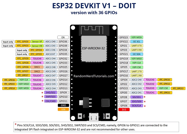
The ESP32 supports many peripherals such as capacitive touch, ADC, DAC, I2C, SPI, UART, I2S, PWM. It is appropriate for IoT Projects and enables Bluetooth communications for Smartphone applications.

ESP32

The ESP32 peripherals include 10 Capacitive sensing GPIOs. They can detect variations in any medium carrying an electric charge. Hence, these capture the variation induced when touching the GPIOs with a finger. You can remove the need for mechanical buttons by integrating these pins into capacitive pads to provide touchscreen functionality.

You can generate variable PWM signals by configuring the 16 channels provided by the ESP32 LED PWM controller. To set a PWM signal, signal frequency, duty cycle, PWM channel, and PWM output GPIOs must be configured in the code. Also, ESP32 has 18 Analog-to-Digital Converter (ADC) channels, 3 SPI interfaces, 3 UART interfaces, 2 I2C interfaces, 2 Digital-to-Analog Converters (DAC), and 2 I2S interfaces.

The ESP32 also features a built-in hall effect sensor that detects changes in the magnetic field in its surroundings.

ESP32 Simulator

ESP32 is open-source software that can simulate the behavior of an ESP32 microcontroller. You can test your code in this software to avoid any unexpected behavior during real-time execution on the actual ESP32 chip.

The ESP32 Simulator software is currently in beta. There are two ESP32 boards as of now:

You can use the ESP32 simulator in 3 ways: Build projects using the ESP32 Arduino Core, Run MicroPython projects, or Simulate bin application files you built on your machine (e.g. using ESP-IDF). Some of the features of ESP32 implemented in the ESP32 simulator software are Processor Core – both cores are simulated, GPIO with interrupts supported, PSRAM4MB external SRAM, UART, I2C, WiFi, ADC, Random Number Generator, and AES/SHA/RSA accelerator.

  • Features like IOMUX, RMT, Timers, and RTC are partially implemented.
  • Features like I2S, SPI, PWM, DMA, Bluetooth, Watchdog and Hall-Effect Sensor have not been simulated yet.

Since the software is open-source, you can also contribute to any feature you might by creating a pull request.

Also for many of the above non-simulated features, there is provision to vote. Based on the results of the vote, the existing community would prioritize the development of the simulation of the most voted-for features.

Getting Started

You can use the ESP32 simulator to run different kinds of applications:

  1. ESP32 Arduino Core projects (including ESP-IDF projects)
  2. MicroPython and CircuitPython projects (examples at https://wokwi.com/micropython)
  3. Rust projects (see https://wokwi.com/rust)
  4. Custom application firmware files (e.g. applications built using the ESP-IDF)
  5. Start from the Arduino-ESP32 Project Template, or from the ESP32 Blink Example.

For more details, please visit ESP32 Simulation | Wokwi Docs

Analog Devices Inc. LTC4451 40V 7A Ideal Diode

Analog Devices Inc. LTC4451 40V 7A Ideal Diode is a high-performance Schottky diode replacement using an integrated N-Channel power MOSFET. It easily ORs power supplies together to increase system reliability and prevent reverse conduction.

The LTC4451 regulates the forward voltage at 15mV to minimize power loss compared to Schottky diodes. Regulation ensures smooth current transfer without oscillation in diode-OR applications. When the power MOSFET is fully enhanced, the RDS(ON) of the transistor is 21mΩ. The power MOSFET is rated for forward conduction up to 7A while dissipating 1.34W. A fast transient response, a high-performance gate driver minimizes forward power dissipation and reverse current. The VCC input allows VIN to work down to ground for low voltage applications. The Analog Devices Inc. LTC4451 is available in a small 16-Lead 2mm × 3mm LQFN Package.

Features

  • Reduces power dissipation by replacing a power Schottky diode with no external components
  • Internal 7A, 21mΩ N-Channel MOSFET
  • 15mV regulated forward voltage
  • 20μA operating current, 0.8μA shutdown
  • Wide 0V to 40V input range with VCC > 2.75V
  • Fast turn-on minimizes voltage droop
  • Fast reverse recovery time minimizes reverse transient current
  • Smooth switchover in diode-OR applications
  • 16-Lead 2mm × 3mm LQFN package

Application Diagram

more information: https://www.analog.com/en/products/ltc4451.html

TOP PCB Companies