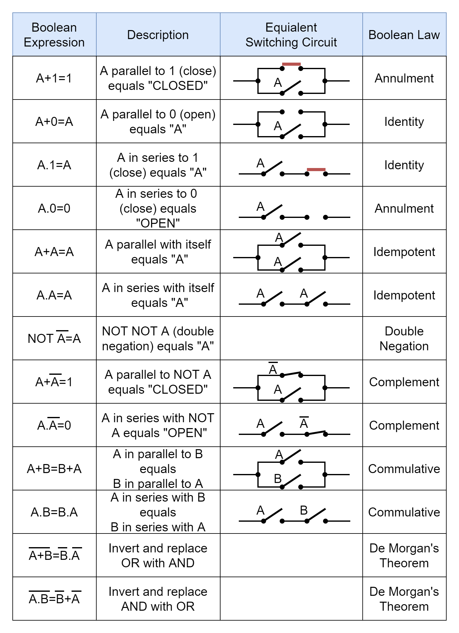
Laws of Boolean Algebra
The digital logic circuits use a Boolean logical data type that can have only two states that are “TRUE” and “FALSE”. These states are also represented by “HIGH” and “LOW” or “1” and “0”, respectively. The digital logic gate’s input and the output state are represented using these values and a combination of logic gates forms a digital logic circuit. As discussed in previous articles, each logical gate performs a logical function that is equivalent to a mathematical function such as a AND gate performs multiplication and an OR gate performs additions, etc. The combined effect of these logic gates in a digital logic circuit is also in logical Boolean data type. Each logic gate logical function and, as such, of the digital logic circuit, can be expressed in a Boolean expression. The Boolean expression can be reduced by a set of algebraic laws and rules. These algebraic laws and rules dealing in logical Boolean data type are referred to as “Laws of Boolean Algebra”.
These Boolean Algebraic laws help in reducing the Boolean expression in order to construct a digital logic circuit based on minimal expression or gates. The laws and theorems employed on a digital logic circuit are based on Boolean data type and similar to the one applied in general mathematics. Therefore, the rules, theorems, or laws employed on Boolean data type are called Laws of Boolean Algebra. In other words, Boolean Algebra is a mathematical technique to analyze digital logic circuits. The technique is generally applied to a complex Boolean expression in order to obtain a minimalist solution. The approach to the minimalist solution can have multiple paths and multiple minimalist solutions. The reduced expression inherits the same logic function of the original/ complex logic circuit but has fewer logic gates involved.
The Boolean expression consists of variables e.g. A, B, and/ or C, etc., and each variable can have two values i.e. “0” or “1”. However, a Boolean expression can have unlimited variables. The Boolean Algebra rules, laws, and theorems are briefly explained hereunder using AND logic.
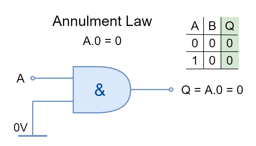
Annulment Law
The input AND’ed by ‘0’ or OR’ed by ‘1’ is stated as Annulment Law. It nullifies or diminishes the effect of the other input
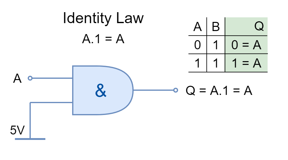
Identity Law
The input AND’ed by ‘1’ or OR’ed by ‘0’ is stated by Identity Law. It keeps the identity of the input.
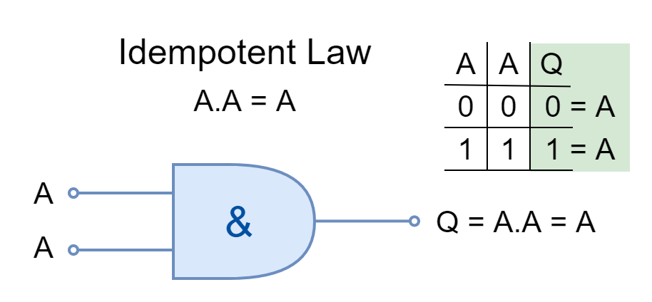
Idempotent Law
The same inputs AND’ed or OR’ed together are stated under Idempotent Law. The logical operation can be applied multiple times without changing the result.
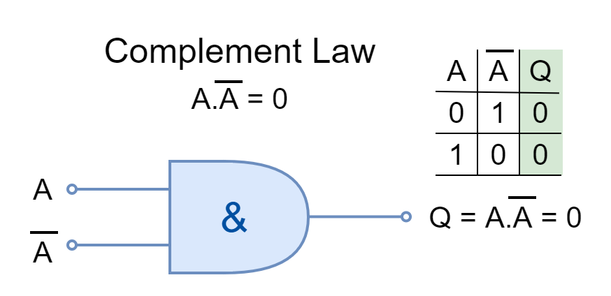
Complement Law
In Boolean Algebra, the complement is the opposite of a logical input such as ‘0’ is the complement of ‘1’ and vice versa. The input and its complement AND’ed or OR’ed together is described by Complement Law.
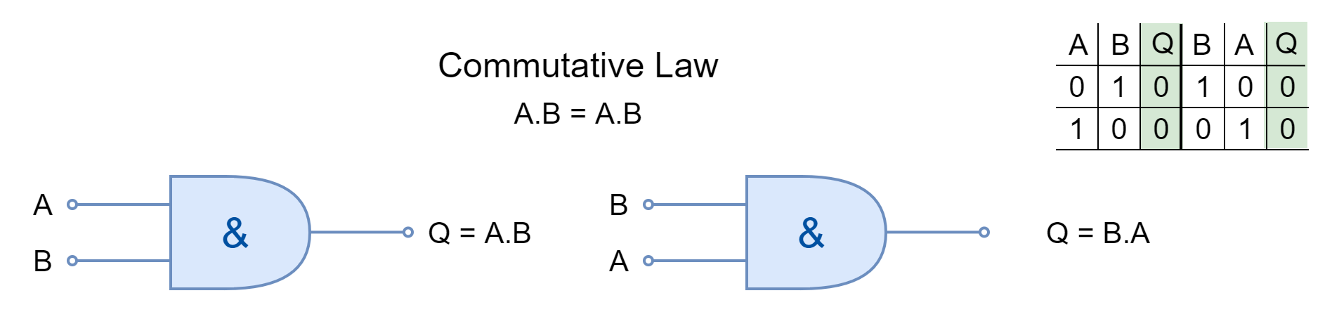
Commutative Law
The commutative law states that changing the order of operands (variables or inputs) does not change the result. In Boolean Algebra, the inputs can be interchanged without changing the results under commutative law.
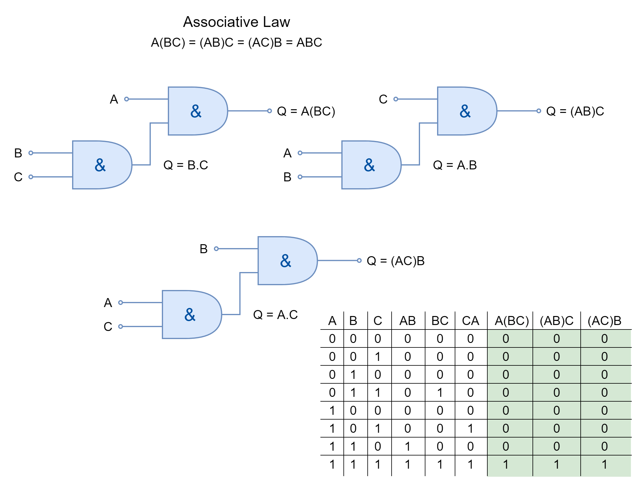
Associative Law
The associative law of multiplication states that the operands grouped differently in multiplication produce the same result. The inputs AND’ed together can be placed interchangeably to form different groups under the Associative Law.
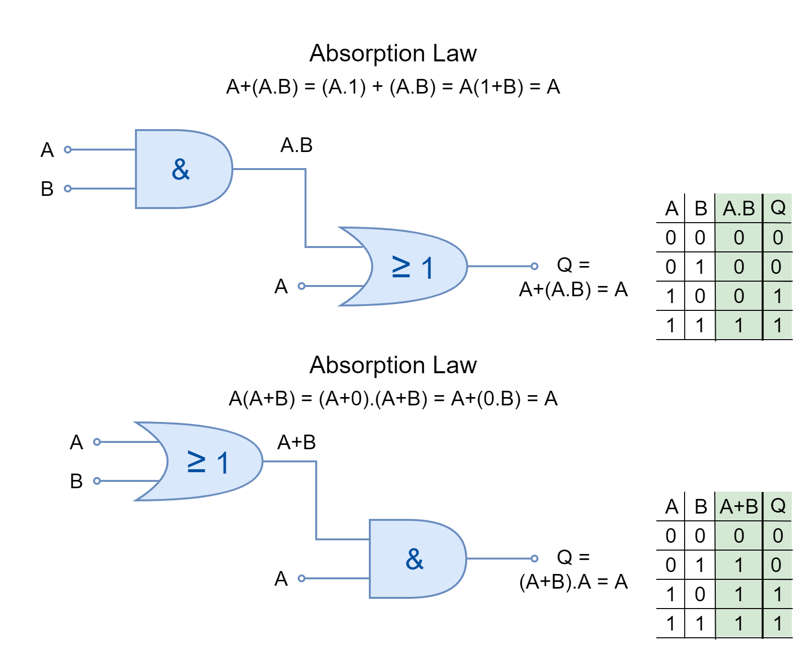
Absorption Law
Using this law, common terms are absorbed to reduce complex expressions to simpler ones.
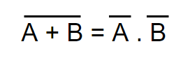
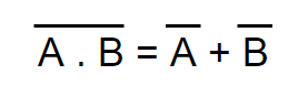
De Morgan’s Theorem
There are two De-Morgan’s theorems which are:
- The NOR of two separate terms together equals AND of individual complements of these two terms. In expression, it is stated as:
- The NAND of two separate terms together equals OR of individual complements of these two terms. In expression, it is stated as:
Boolean Postulates
There are some mathematical laws that are helpful in the reduction of Boolean expressions. These Boolean postulates are listed below.
AND of 0 with itself, always equals “0”
0.0 = 0
AND of 1 with itself, always equals “1”
1.1 = 1
AND of 1 with a 0, always equals “0”
1.0 = 0
OR of 0 with itself, always equals “0”
0+0 = 0
OR of 1 with a 0, always equals “1”
1+0 = 1
OR of 1 with itself, always equals “1”
1+1 = 1
The inverse of a 0, always equal to “1”
![]()
The inverse of a 1, always equal to “0”
![]()
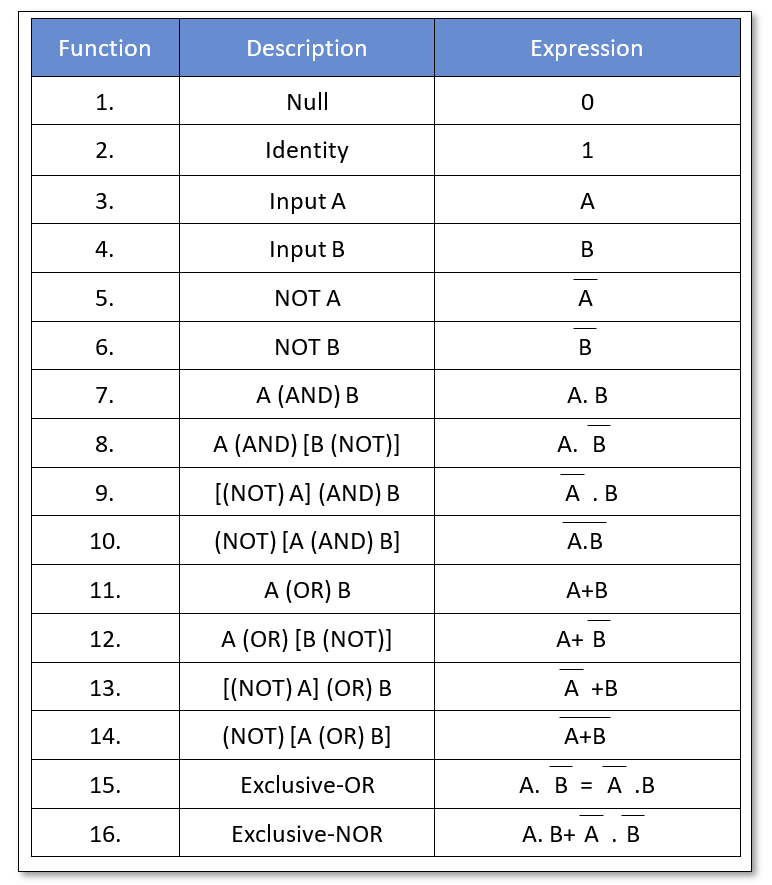
Boolean Algebra Functions
The basic logic gates i.e. AND, OR, and NOT can render the following sixteen (16) Boolean functions using above stated laws, rules, theorems, etc.
Boolean Algebra Example No. 1
The following expression is simplified using above stated Boolean Algebra laws:
(A+B)(BC)
Steps:
(A+B)BC
Apply: Distribution
BCA+ BCB
Apply the Idempotent Law: A.A = A
BCA+BC
Apply the Absorption Law: A+AB=A
BC
The expression (A+B)(BC) can be simplified into BC only.
Boolean Algebra Example No. 2
The following expression is simplified using above stated Boolean Algebra laws:
(A+B)(A+B+1)
Steps:
(A+B)(A+B+1)
Apply: Identity Law: A+1=1
(A+B)(1)
Apply: Identity Law: A1 = A
The expression (A+B)(A+B+1) can be simplified into (A+B) only.
Conclusion
- The Boolean Algebra deals with Boolean logic data type in which each variable can have only two possible states i.e. TRUE (1) or FALSE (0).
- The set of rules, laws, and theorems based on Boolean logic data type is applied to reduce complex Boolean expressions to simpler ones.
- The Laws of Boolean Algebra are briefly stated in below table: