Full Wave Rectifier Using Single Supply OPAMP

This is a Full wave rectifier project built using MAX44267 dual OPAMP which provides true zero output with a single supply. The circuit converts Bipolar/AC input into full-wave output. CN1 is provided for sinewave input, CN2 helps to connect the power and output. Operating supply 15V DC, D1 power LED.

The MAX44267 precision, low-noise, low-drift dual operational amplifier offers true-zero output that allows the output to cross zero maximizing the dynamic range of an ADC and increasing resolution. In addition, the input common-mode range extends from +13.5V down to -12V. The MAX44267 integrates charge-pump circuitry that generates the negative voltage rail in conjunction with external capacitors. This allows the amplifier to operate from a single +4.5V to +15V power supply, but it is as effective as a normal dual-rail ±4.5V to ±15V amplifier. The architecture eliminates the need for a negative power-supply rail, saving system cost and size. The MAX44267 is unity-gain stable with a gain-bandwidth product of 5MHz. The device features low offset voltage of 50μV (max), drift of 0.4µV/°C (max), and 200nVP-P noise from 0.1Hz to 10Hz. The low offset and noise specifications and wide input common-mode range make the device ideal for sensor transmitters and interfaces.  Varying the external charge pump capacitors enables the charge-pump noise to be minimized.

Features

  • Operating power Supply 15V DC @ 10mA
  • Input Signal 100mV to 4V Peak to Peak
  • Input Frequency Response 1Hz to 10Khz
  • 2Khz Full wave output from 1Khz Sinewave
  • CN1 2.54 mm Male Header Connector for Input Signal
  • D1 Power LED
  • CN2 Signal Output and Power Input
  • PCB Dimensions 30.64 x 19.69 mm

Schematic

Parts List

NO.QNTY.REF.DESC.MANUFACTURERSUPPLIERPART NO
11CN12 PIN MALE HEADER PITCH 2.54MMWURTHDIGIKEY
21CN24 PIN MALE HEADER PITCH 2.54MMWURTHDIGIKEY732-5317-ND
32C1,C310uF/25V SIZE 1206MURATA/YAGEODIGIKEY732-5315-ND
44C2,C4,C5,C60.1uF/50V SMD SIZE 0805MURATA/YAGEODIGIKEY
51C715PF/50V SMD SIZE 0805MURATA/YAGEODIGIKEY
61C80.022UF/25V SMD SIZE 0805MURATA/YAGEODIGIKEY
71D1LED SMD SIZE 0805OSRAMDIGIKEY475-1278-1-ND
81D21N4148 SMDMICROCHIPDIGIKEY494-JAN1N4148UR-1
91L1F-BID 80 Ohms/100MhzTDKDIGIKEY445-2187-1-ND
101R12.2K 5% SMD SIZE 0805MURATA/YAGEODIGIKEY
111R220K 1% SMD SIZE 0805MURATA/YAGEODIGIKEY
121R310K 1% SMD SIZE 0805MURATA/YAGEODIGIKEY
131R460.4K 1% SMD SIZE 0805MURATA/YAGEODIGIKEY
141R530.1K 1% SMD SIZE 0805MURATA/YAGEODIGIKEY
151U1MAX44267MAXIMMOUSER700-MAX44267AUD+

Connections

Waveforms

Input (green) and Output (yellow) of a 150Hz sine wave

Gerber View

Photos

Video

MAX44267 Datasheet

6V – 2.5Ah Sealed Lead-Acid Battery Charger

This dual-level float charger was designed for a 6V (three 2V cells) 2.5Ah battery. D2 LED was added for visual indication of charge completion, D3 indicates power, D4 LED presents overcharge condition, etc. 6V lead-acid battery charger is built using the UC3906 chip. UC3906 contains all of the necessary circuitry to optimally control the charge and hold cycle for sealed lead-acid batteries. UC3906 IC monitors and controls both the output voltage and current of the charger through three separate charge states; a high current bulk-charge state, a controlled over-charge, and a precision float-charge, or standby state. Optimum charging conditions are maintained over an extended temperature range with an internal reference that tracks the nominal temperature characteristics of the lead-acid cell. A typical standby supply current requirement of only 1.6mA allows these ICs to predictably monitor ambient temperatures. Separate voltage loop and current limit amplifiers regulate the output voltage and current levels in the charger by controlling the onboard driver. Voltage and current sense comparators are used to sense the battery condition and respond with logic inputs to the charge state logic.

A charge enable comparator with a trickle bias output can be used to implement a low current turn-on mode of the charger, preventing high current charging during abnormal conditions such as a shorted battery cell. Other features include a supply under-voltage sense circuit with a logic output to indicate when input power is present. In addition, the over-charge state of the charger can be externally monitored and terminated using the over-charge indicate output and over-charge terminate input.

Note: The circuit is configured to charge 6V – 2.5 to 4.5Ah Battery. Higher current and voltage batteries can be charged by changing resistors values, refer to the datasheet of UC3906 for the same.

Do not populate the following components: CN3, R14, R16, R17, R18 they are optional for microcontroller interface/control.

Features

  • Input Supply Voltage  0V to 13V DC, 1Amp – 2Amp
  • Bulk Charge Rate 500mA
  • 5AH To 4.5AH Battery Can be Charged
  • Start-up Trickle Current 10mA
  • Start-up voltage 5.1V
  • Bulk to OC Transition Voltage 7.125V
  • OC Voltage 5V
  • Float Voltage 7.0V
  • Float to Bulk Transition Voltage 6.3V
  • OC Terminate Current 50mA
  • On-Board Power LED
  • Over Charge LED
  • Fully Charged LED

Schematic

Parts List

NOQNTYREF.DESC.MANUFACTURERSUPPLIERPART NO
11CN12 PIN SCREW TERMINAL PITCH 5.08MMPHOENINXDIGIKEY277-1247-ND
21CN22 PIN SCREW TERMINAL PITCH 5.08MMPHOENINXDIGIKEY277-1247-ND
35C1,CN3,R16,R17,R18DNP
43C2,C3,C40.1uF/50V SMD SIZE 0805MURATA/YAGEODIGIKEY
51D11N4007 SMD SMC DIODEDIGIKEY1655-1N4007FLTR-ND
61D23MM LED GREENAMERICAN OPTODIGIKEY2460-L314GT-ND
71D33MM LED YELLOWAMERICAN OPTODIGIKEY2460-L314YD-ND
81D43 MM LED REDAMERICAN OPTODIGIKEY2460-L314ET-ND
91Q1TIP32BONSEMIDIGIKEYTIP32BOS-ND
101R10.5E 1% SMD SIZE 2512MURATA/YAGEODIGIKEY
112R2,R11220E 1% SMD SIZE 0805MURATA/YAGEODIGIKEY
121R375K 1% SMD SIZE 0805MURATA/YAGEODIGIKEY
132R4,R7100K 1% SMD SIZE 0805MURATA/YAGEODIGIKEY
141R514K 1% SMD SIZE 0805MURATA/YAGEODIGIKEY
151R6470E 1% SMD SIZE 0805MURATA/YAGEODIGIKEY
161R88.2K 1% SMD SIZE 0805MURATA/YAGEODIGIKEY
173R9,R13,R151K 1% SMD SIZE 0805MURATA/YAGEODIGIKEY
181R10390K 1% SMD SIZE 0805MURATA/YAGEODIGIKEY
191R1243K 1% SMD SIZE 0805MURATA/YAGEODIGIKEY
201R14DNODIGIKEY
211U1UC3906 TIDIGIKEY296-11621-ND
221U2LM393ONSEMIDIGIKEYLM393EDR2GOSCT-ND
231U2 SOCKETDIP 16 IC SOCKETADAM TECHDIGIKEY2057-ICS-316-T-ND

Connections

Gerber View

Photos


UC3906 Datasheet

Engineering Samples of Ultra-Low Power AON1100 Chip and Development Kit Now Available

AONDevices, Inc., a provider of ultra-low power, high-performance processors for a new era of edge AI, today announced that engineering samples of its new AON1100™ processor are now available. The AON1100 Edge AI processor enables unprecedented sensing capabilities in battery-powered always-on devices that need to support local wake words, voice commands, sound event detection, context detection, and sensor fusion at high accuracy – all while maintaining industry-leading low power consumption that extends battery life, which results in a better end-user experience.

Real World Recognition

The AON1100 is the industry’s first and only ultra-low power, a multi-modal solution that enables simultaneous, extremely accurate recognition of multiple voice commands and sound events – such as a baby crying or a car backfiring – using a single microphone.

The AON1100 also simultaneously detects specific motion patterns, such as walking or falling. When used in phones, headsets, wearables, game controllers, vehicles, or smart home appliances, the AON1100 enables natural human-machine interface at the device level without sending any data to the cloud, improving the user experience and guaranteeing privacy.

AON1100 features two cores, AONVoice™ and AONSens™, which are based on AONDevices’ proprietary neural network technology. AONVoice delivers 90% accuracy in 0 dB SNR conditions. Including front-end processing and all required memory, AONVoice core consumes less than 150µW proven in 40nm ULP silicon. This power is measured in 100% constant speech conditions.

Machine Learning’s New Era

“The AON1100 is a testament to AONDevices’ unparalleled ability to innovate across algorithms, systems and silicon,” said Mouna Elkhatib, CEO of AONDevices. “We are engaged with several tier 1 customers in key markets. With engineering samples and development kits now available, we can support OEM customers looking for complete solutions that don’t sacrifice privacy or trade accuracy for power.

In addition, we continue to enable key silicon partners and OEMs with IP core licenses. We are enabling a wide range of new voice, audio and sensor use cases – and we can’t wait to see what new capabilities our customers will bring to market next.”

AONDevices is a partner of the tinyML Foundation – a global industry group focused on nurturing the fast-growing branch of ultra-low power ML technologies and approaches at the edge – and embraces the vision set forth by the organization.

Commenting on the industry, Evgeni Gousev, senior director at Qualcomm and chairman, board of directors of the tinyML Foundation, noted that,

“At the tinyML Foundation, we envision this new world as having trillions of distributed intelligent devices enabled by energy-efficient machine learning technologies that sense, analyze and autonomously act together to create a healthier, more sustainable environment for all.”

Pricing, Availability and Demos

Engineering samples of the AON1100 chip are available now. AONVoice and AONSens cores are also available for licensing as IP cores for integration in an SoC to high-volume customers. Contact info@aondevices.com for pricing and additional information. AONDevices will demonstrate its AON1100 Edge AI processor at CES 2022 from January 5-8 in Las Vegas at booth #61709 in Eureka Park.

Please connect with AONDevices at info@aondevices.com to schedule an appointment.

Toshiba TCK12xBG 1A Load Switch ICs

Toshiba TCK12xBG 1A Load Switch ICs are designed for general power management with a slew rate control driver. The TCK12xBG ICs feature ultra-low quiescent current, low switch ON resistance, and a wide 1.0V to 5.5V input operation voltage range. Additionally, the devices provide a quiescent current of 0.08nA and an output current up to 1.0A.

The Toshiba TCK12xBG 1A Load Switch ICs are housed in a 0.35mm pitch ultra-small WCSP4G package (0.645mm x 0.645mm, t: 0.465mm max.) with backside coating that protects from external damage. The TCK12xBG ICs are ideal for portable applications that require high-density board assembly and ultra-low power consumption, such as wearables, smartphones, and IoT modules.

Features

  • Wide input operation voltage range of VIN = 1.0V to 5.5V
  • Built-in slew rate control driver
  • High output current of IOUT = 1A
  • Ultra small Quiescent current at IQ = 0.08nA at VIN = 5.5V, VCT = 0V, IOUT =0mA
  • Built in slew rate control driver
  • Low ON resistance
    • RON = 58mΩ (typ.) at VIN = 3.3V, IOUT = -0.5A
  • Low standby current (OFF state) : IQ(OFF)+ISD(OFF)=13nA (typ.)
  • IN (OPR)= 1.0V to 5.5V
  • Built-in auto-discharge (TCK127BG)
  • Active low (TCK128BG), Active high (TCK126BG, TCK127BG)
  • WCSP4G Ultra small package with back side coating (0.645mm x 0.645mm, t: 0.465mm max.)

more information: https://toshiba.semicon-storage.com

Meet GL-S10 – A $24.90 Bluetooth IoT Gateway For BLE to MQTT Transmission

Building a simple and cost-efficient system for BLE and cloud server communication can be quite tasking considering the availability of network environments requiring either BLE, WiFi, Ethernet, or a combination of these input/output protocols. That is why GL.iNet, known for OpenWrt WiFi routers, has released its newest model, GL-S10 as a BLE to MQTT cloud server over WiFi or WAN support.

The GL-S10 is an IoT gateway with BLE and WiFi supports protocols for transmitting BLE messages to the cloud without the need for a web admin panel. Its BLE is built around GAP and GATT standards and certification, capable of functioning as either a Master or Slave server to talk with other available BLE devices within the coverage area. The GL-S10 can also communicate via WiFi as a station for parent access or the Internet via its Ethernet (WAN) port and this makes it a cost-effective solution. You should see it as your favorite for IoT communications.

The GL-S10 also has an onboard MQTT client to access any available standard MQTT server to transmit BLE broadcast data to the cloud destination. Apart from its support for an onboard Bluetooth module with a BLE communication distance of up to 80 meters, the device is said to support 802.3at/af standard PoE input supply.

Key Features And Specifications of GL-S10 include:

  • ESP32-DOWD: Dual-core Xtensa 32-bit LX6 microprocessor
  • 8MB PSRAM, 520KB SRAM
  • 4MB Nor-Flash
  • Bluetooth V4.2, BLE (with GAP and GATT standard)
  • IEEE 802.11 b/g/n WiFi @ 2.4GHz (Wi-Fi Speed 150Mbps)
  • 10/100M WAN (Megabit Ethernet) port
  • External antenna
  • 5V/1A DC Input (Micro USB) or PoE Power Input (802.3at/af standard)
  • 3x LEDs (Power, Internet, BLE), 1x Reset Button
  • Power consumption: <0.5W (Typical)
  • Operating Temperature: 0~40°C (32~104°F)
  • Dimension: 57 mm x 57 mm x 25mm
  • Weight: 53.6g

As for device configuration, GL-S10 requires that you download and install the GL-S10 tool application on your mobile phone, and use the application to filter, identify the device, deploy and configure your BLE to MQTT protocols. See the User manual for more information on that including OTA upgrade, Network configuration, Data configuration, Cable configuration, etc. Alternatively, you can set up GL-S10 firmware and build applications for GL-S10 based on your own project requirements and settings with the aid of its firmware compilation guide.

GL-S10 is already available for custom development to meet the requirements of MQTT servers, you just need to request via a sales email address provided on the product page.

The GL-S10 sells for $24.90 on the GL.iNet store. You’ll be required to pay an extra $5 if you want a BLE beacon alongside the gateway.

Radxa CM3-Beta – An Alternative For Raspberry Pi CM4

Shenzhen-China based Open Source hardware manufacturer, Radxa has launched its system on module (SoM), Radxa CM3 which the company says is “a drop-in-replacement for Raspberry Pi CM4” for open hardware developments and deployments.

The Radxa CM3 is built on Rockchip RK3566 SoC with a 2GHz, quad Cortex-A55 core with an ARM G52 2EE graphics processor with OpenGL ES 3.2, OpenCL 2.0 and Vulkan 1.1 support; and a Neural network processor (coprocessor) with 0.8 TOPS performance rating. The Radxa CM3 SoM also features DRAM of up to 8GB, 128GB eMMC storage, WiFi 5/BT 5, display interfaces with dual support, and other resources which are furnished on a three 100pin B2B connector.

According to the company, the CM3 has been tested with multiple CM4 carrier boards including the Raspberry Pi CM IO board and it turns out that the boards can work well with the CM3 without the need for tweaks.

Key Features And Specifications Of Radxa CM3:

  • Rockchip RK3566, Quad core Cortex-A55 (ARM v8) 64-bit SoC @ 2.0GHz
  • Options for 1GB, 2GB, 4GB or 8GB LPDDR4-3200 SDRAM + ECC; Options for 0GB, 8GB, 16GB, 32GB, 64GB, 128GB eMMC Flash, 250MBytes/s (Peak eMMC bandwidth)
  • Single +5v PSU
  • Option for WiFi5/BT5
  • Gigabit Ethernet PHY(RTL8211F), IEEE 1588 support (optional)
  • 1x high-speed USB 2.0 port
  • 1x USB 3.0 port (5Gbps)
  • 1x PCIe 1-lane Host, Gen 2 (5Gbps)
  • 2 x SATA ports, one shared with USB 3, one shared with PCIe
  • 1 x HDMI (up to 4K60)
  • 2 × 4-lane MIPI DSI display port (MIPI DSI0, MIPI DSI1), 1 x 4-lane LVDS support (shared with MIPI DSI0)
  • 1 x eDP up to 4K60
  • 1 × 2-lane MIPI CSI camera port
  • 1 × 4-lane MIPI CSI camera port
  • 1 x SDIO 3.0
  • Audio Codec
  • 50 × GPIO supporting either 1.8v or 3.3v signaling and peripheral options: Up to 8x UART, Up to 8x I2C, Up to 4x SPI, 1x SDIO interface, 1x PCM, Up to 8x PWM channels, 2x ADC, 3x 100Pin B2B connector
  • Dimension: 55mm × 40mm × 4.7mm

Radxa has also made available its CM3 IO board, a dedicated board for makers to use the extra features of CM3 at deployment.

Here are some of the features of the CM3 IO Board:

  • Multiple display interfaces support: HDMI, 2x MIPI DSI, eDP, dual display (at the same time)
  • 2x MIPI CSI support (at the same time)
  • 1x PCIe card
  • ATX case mount support
  • Up to 2x SATA (one shared with USB3.0 while the other shared with PCIe 2.0)
  • Operating System: Ubuntu, Debian, and Android
  • Dimension: 170 mm x 85mm

The Radxa CM3-beta is available for hardware developers doing real testing on projects. Radxa has provided a Github repository for free beta hardware applications.

Further information on the Radxa CM3-beta is available on the Radxa forum and the Wiki page.

$25 DSTIKE USB KEEPER Now Available For Order

Independent hardware Developer, Travis Lin, has just designed and launched his newest device with the product name, DSTIKE USB KEEPER. The board is designed to function as an input device to a personal computer (PC) and an integrated USB HID Arduino board for project developments.

The DSTIKE USB KEEPER can operate as a keyboard for control and commands input when connected to a PC, as well as a USB for reading stored scripts from TF cards and displaying them via a menu system via an OLED screen. It is equally a replacement for the Arduino Leonardo development board, suitable for learning Arduino and developing solutions requiring the board to serve as a USB interface device.

The board is equipped with a 3-way toggle switch for switching and selecting board functions such as opening and writing on a notepad, opening cmd and inputting clean PC command, opening a website, and, reading and showing SD card including information like card type and storage size. Lin also claimed that the board opened a 40 music YouTube website in a demo program. So, with these capabilities, you would likely do more interesting work with the board by programming and tweaking alongside its featured 5x GPIOs headers.

The board is powered by a 16MHz ATmega32u4 MCU with inbuilt USB communication. It is capable of being recognized by a connected PC as either a keyboard or a mouse, which allows for its use with the 3-way toggle switch and the OLED screen for selecting the User’s command.

Key Features and Specifications of the DSTIKE USB KEEPER:

  • Microchip 8-bit AVR® RISC;
    • ATmega32u4, 16MHz @ 2.7-5.5 volt operation,
    • 1 KB EEPROM, 32 KB Flash,
    • 2.5 KB SRAM,
    • 12-channel 10-bit A/D-converter,
    • USB 2.0, JTAG (for on-chip-debug)
  • 1.3 OLED screen
  • USB-A
  • 5x GPIOs
  • SD holder
  • No SD card
  • Dimension: 3cm x 3cm x 7cm

As a guide and safety measure on the use of the DSTIKE USB KEEPER, Lin noted that the “Atmega32u4 is a simple 16Mhz MCU. It has limited memory to use. The demo program has already occupied 94% of memory. I do not suggest you write a more complex program. Once the memory is overflowed this board may not be recognized by the PC. Then you have to reflash the bootloader.”

The board’s documentary on source code and design files are available on Travis Lin’s Github repository. If you are interested in the board, you can place an order for it on DSTIKE’s Store or Tindie for just $25. Other useful details can also be found on those sites.

Introducing Inforce 68A1, a powerful new system-on-module designed to enable advanced IoT vision system devices

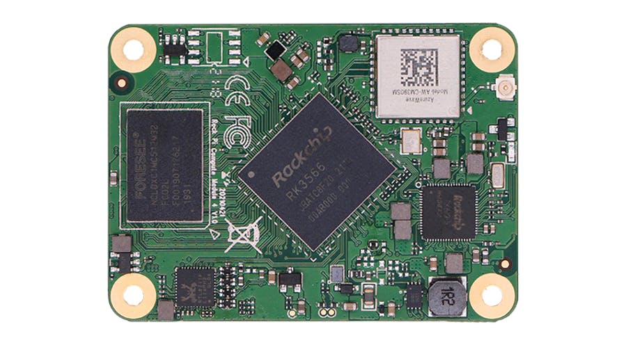
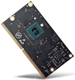
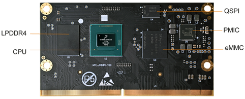
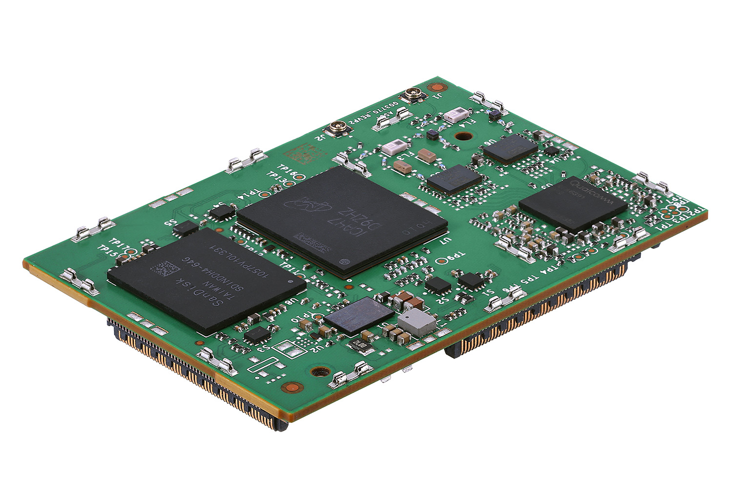
SMART Wireless Computing, Inc., an SGH company and leading provider of edge computing embedded solutions, today announced the Inforce 68A1 system-on-module (SoM), a powerful new tool based on one of the latest and most advanced IoT solutions from Qualcomm Technologies, Inc., the Qualcomm® QCS8250 system-on-chip (SoC), which is designed to provide high performance for compute-intensive network edge Internet of Things (IoT) camera applications. The Inforce 68A1 SoM combines support for multiple high-resolution 8K or 4K cameras with complex artificial intelligence (AI) inferencing at the edge to enable smart camera systems, high-performance conferencing/collaboration devices, connected healthcare, and intelligent retail devices.

The Inforce 68A1 SoM provides exceptionally high-resolution video capabilities, including processing 4K60 Ultra HD content for multiple cameras and displays concurrently, plus high bandwidth connectivity via 802.11ax DBS Wi-Fi 6E and Bluetooth 5 for connected camera networks. The module makes use of Qualcomm Technologies’ high-performance Qualcomm® Hexagon DSP and Qualcomm® AI Engine to efficiently run heterogeneous deep learning workloads and neural networks for high-performance, on-device AI inferencing used in video analytics and to improve the user experience.

Video Conferencing Use Case

Never before has reliable video conferencing been more in demand, with companies across the globe embracing AI technology to simplify audio-visual collaboration as remote working becomes more widely adopted. By integrating the Inforce 68A1 SoM into enterprise video conferencing solutions, businesses can deliver content, connect and interact effortlessly, from anywhere, for a flawless video experience.

Medical Use Case

Similarly, applying computer vision AI to medical fields, such as portable ultrasound machines, can help provide remote anatomical identification with fewer clicks and increased accuracy. This anatomical identification also helps automate measurements, make them more reproducible, and can give medical professionals tools to improve patient care, and bolster the resources of hospitals that lack adequate medical imaging resources.

Retail Use Case

As retailers look to keep up with changing landscapes, the introduction of AI video content analysis solutions presents an entirely new level of data processing which leads to a deeper understanding of consumer attitudes, preferences, and buying habits. By integrating the Inforce 68A1 SoM into retail camera systems and self-checkout technology, retailers can improve merchandising and enhance customer behavior and engagement while providing a seamless, low-contact shopping experience.

“With vast progress being made in AI and machine learning, applications that previously involved manual intervention can now be automated or enhanced to solve some of the most common challenges in our day-to-day lives,” said Todd Wynia, vice president, product marketing at SMART Wireless Computing. “Our application-ready embedded platforms are at the core of this, providing multiple options for global IoT connectivity, multimedia capabilities, and powerful edge computing power, revolutionizing the way we communicate, shop and approach healthcare, among many other possible applications.”

“The Qualcomm QCS8250 SoC targets high performance, on-device camera applications in retail video analytics, connected healthcare, digital signage and enterprise video collaboration,” said Siddhartha Franco, director, business development, Qualcomm Technologies, Inc. “This device is optimized for maximum performance while balancing power efficiency with support for Wi-Fi 6 and 5G connectivity. The SMART Wireless Inforce 68A1 SoM brings technology at the connected intelligent edge to a broader ecosystem of developers, helping reduce the time and risks involved with integrating premium tier AI performance into their edge camera solutions.”

This latest module includes an Android 10 board support package with the Qualcomm Technologies’ software development kits, including Hexagon SDK and Qualcomm® Neural Processing Engine SDK, enabled.

Technical Specifications and Application Benefits

  • The Qualcomm QCS8250 SoC at the heart of the Inforce 68A1 SoM integrates:
    • The Qualcomm® Kryo 585 CPU is one of the company’s most advanced processors for IoT applications that provides excellent performance and multi-tasking.
    • The Qualcomm® Adreno 650 GPU provides a highly efficient graphics core, delivering twice the performance of the previous generation platform, and 60 percent greater power efficiency.
    • The Hexagon 690 DSP runs power efficient machine learning with quad-threaded Scalar performance and twice the Vector eXtensions performance
    • A dedicated computer vision hardware block and new Hexagon Tensor Accelerator delivering 15 TOPS of AI performance
    • The Qualcomm® Spectra 480 ISP enables image capture at 64MP@30fps ZSL with no shutter lag and quick autofocus.
    • The Adreno DPU995 Display Engine enables dual concurrent display content at HEVC 10bit and VP9 decode.
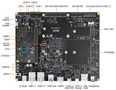
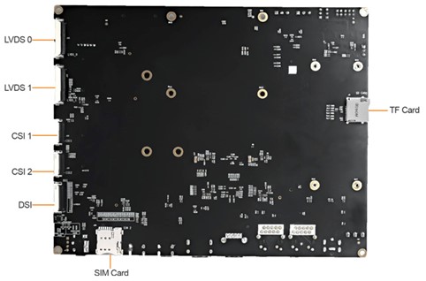
    • Wired and wireless connectivity options include Wi-Fi 6, 5G, Bluetooth 5.1 RF front-end technologies and dual USB 3.1.
    • A secure processing unit enables secure boot, DRM and content protection creating a secure environment for the camera system.
  • The Inforce 68A1 SoM leverages PMIC regulators for large power requirements and on-board power management.
  • On-board memory and storage includes 8GB DDR5 RAM and 64GB Universal Flash Storage (UFS) for fast multitasking.
  • Designed to fit into and power ultra-thin applications, the small form factor SoM measures just 35 mm x 53 mm (7.5 mm profile).
  • Electromagnetic interference (EMI) shielding provides radio frequency noise protection, while also improving heat dissipation to improve performance.
  • A development kit based on this SoM offers functionality to help developers create and optimize their products quickly, cost effectively and with lower risk.

Starting in December, customer samples will be available to order at www.smartwirelesscompute.com priced at $399 for the SoM and $749 for the development kit, which includes a SoM, evaluation carrier board with IO, and a starter kit that includes a power adapter and cable.

Weller’s Zero Smog 6V Fume Extraction System connects up to 8 workbenches

Weller Tools, the world’s No.1 brand in hand soldering solutions, is pleased to announce that its Zero Smog 6V Fume Extraction System can connect up to eight soldering workbenches.

The Zero Smog 6V (ZS 6V) Fume Extraction System is user-friendly with quick and simple installation and filter exchange. It has a low noise emission level and is small and convenient to locate within the work area. The high-quality components used in the ZS 6V result in low servicing requirements and long system life.

To increase filter lifetime and save on energy, the ZS 6V is fitted with constant flow control (CFC) – depending on the number of connected workplaces. To extend the capacity an external pre-filter can be fixed directly to the ZS 6V.

One of Weller’s largest extraction units, the ZS 6V features a powerful 615m3/hr (362 CFM) flowrate. The system’s large filter contains up to 13kg (29lbs) of granulated filtration media for an exceptionally long filter life.

more information: https://www.weller-tools.com/professional/EUR/en/Filtration/3D+printer+vapours/Zero+Smog+6V+fuer+Kleberdaempfe

MYIR Launched i.MX 8M Plus SoM with AI/ML Capabilities

After the former release of NXP i.MX 8M based MYC-JX8MX and i.MX 8M Mini based MYC-C8MMX System-on-Modules, MYIR has launched another advanced SoM MYC-JX8MPQ based on quad Arm Cortex-A53/M7 i.MX 8M Plus processor which is NXP’s first i.MX processor with a built-in 2.3 TOPS Neural Processing Unit (NPU) for extensive Artificial Intelligence (AI) and Machine Learning (ML) capabilities. The i.MX 8M Plus also has integrated 1080p Video Processing Unit (VPU), 2D/3D Graphics Processing Unit (GPU), dual ISPs (Image Signal Processors) and audio DSP to provide a perfect solution for machine learning and vision, advanced multimedia, and industrial automation applications.

MYC-JX8MPQ CPU Module

Measuring 82mm by 45mm, the MYC-JX8MPQ CPU Module takes full features of the i.MX 8M Plus processor and carries out most of the I/O signals to and from the CPU Module through a 0.5mm pitch 314-pin MXM 3.0 gold-finger-edge-card connector. It has 3GB LPDDR4, 8GB eMMC and 32MB QSPI flash default memory and storage configuration as well as integrated PMIC. It is capable of running Linux OS and provided with plenty of software resources and demos.

MYD-JX8MPQ Development Board Top-view (delivered with installed heatsink by default)

MYIR offers MYD-JX8MPQ Development Board for evaluating the MYC-JX8MPQ CPU Module, which is a complete evaluation platform with rich peripheral set and connectivity including UARTs, USB 3.0 Host, OTG, dual Gigabit Ethernet, dual CAN, dual M.2 Sockets (one for 5G LTE Module and one for PCIe SSD), one extension header for connecting with MYIR’s MY-WF005S WiFi/Bluetooth module and one UART/I2C/SPI/GPIO extension header which is compatible with Raspberry Pi interface, Micro SD card slot, dual MIPI-CSI Camera Interfaces, LVDS /MIPI-DSI display interface, Audio, HDMI, etc. MYIR can also offer design services to help customize the base board according to customers’ requirements.

MYIR offers commercial and industrial options for CPU Modules and Development boards. The prices are economic. Discount is to be offered for volume quantities.

Product Item Part No. Retail Price
MYC-JX8MPQ CPU Module MYC-JX8MPQ-8E3D-160-C $115/pc
MYC-JX8MPQ-8E3D-160-I $129/pc
MYD-JX8MPQ Development Board MYD-JX8MPQ-8E3D-160-C $335/pc
MYD-JX8MPQ-8E3D-160-I $349/pc

More information about above new products can be found at:

TOP PCB Companies