GeneSiC Semiconductor 3300V SiC MOSFETs

GeneSiC Semiconductor 3300V SiC MOSFETs offer fast and efficient switching with reduced ringing in an optimized package with a separate driver source pin. The 3300V SiC MOSFETs are designed to be compatible with commercial gate drivers and provide ease of paralleling without a thermal runaway. The 3300V SiC MOSFETs deliver low conduction losses at all temperatures, allowing superior robustness and system reliability.

Features

  • Softer RDS(ON) v/s temperature dependency
  • LoRing™ – electromagnetically optimized design
  • Smaller RG(INT) and lower QG
  • Low device capacitances (COSS CRSS)
  • Industry-leading UIL and short-circuit robustness
  • Robust body diode with low VF and low QRR
  • Normally off-stable temperature up to 175°C
  • Optimized package with separate driver source pin

Applications

  • Traction
  • Solar string inverters
  • EV- fast chargers
  • Pulsed power
  • Switched-mode power supply
  • Energy storage
  • Solid-state transformers
  • Solid-state circuit breakers

more information: https://www.genesicsemi.com/sic-mosfet/G2R1000MT33J/G2R1000MT33J.pdf

MangoPi-MQ1, a RISC-V Linux Capable Dev Board For Allwinner D1s Is Coming Soon For Under $10

Cost and size are two things you consider when choosing components for portable systems, after functionality and performance. Not too long ago, we saw the Sipeed’s Lichee RV that was launched for about $20 and designed to compete with the $99 Nezha SBC. Now, MangoPi has released an open-source development board called MangoPi-MQ which sells for even a cheaper price of $10.

The MangoPi-MQ also called Sparrow is a mini-compact, low-cost and high-performance RISC-V Linux-based development board for Allwinner D1s chip. The development board is a 40mm x 40mm condensed board with minimal resources for reduced systems complexity. It has a clock speed of 1.0 GHz alongside 64MB RAM, and a 5V/2A power supply via OTG or USB-C 2.0 connector. The board also features an LVDS for video support as well as a built-in microphone for audio, WiFi 802.11 b/g/n for networking and micro-SD and SPI NAND for storage.

The D1s SoC is a low-cost chip for Artificial Intelligence of Things (AIoT) for smart packages, signals, and data codec processes. It runs a 64bit RISC-V XuanTie-C906 processor of Alibaba T-Head division with 64MB DDR2, and features audio and video coding and decoding protocols which support H.264, H.265, MPEG-1/2/4, JPEG video formats and ADC/DAC/I2S/PCM/DMIC/OWA audio interfaces. The D1s chipset is Linux compatible and suitable for automotive applications and smart home and industrial solutions.

Key Features and Specifications:

  • SoC: D1s @ 1.0Ghz, 64MB DRAM
  • DC 5V/2A (via OTG or USB-C connector)
  • LVDS
  • Inbuilt microphone, I2S
  • WiFi 802.11 b/g/n
  • Micro-SD
  • SPI NAND
  • 1x USB-C 2.0 Host
  • 1 x USB-C OTG
  • 15P universal Raspberry Pi DSI FPC row seat
  • 40P universal row seat (RGB FPC)
  • 6P universal capacitive touch row seat (FPC)
  • 24 Pin DVP interface
  • 2x 22 Pin extension header
  • Boot button
  • Reset button
  • Dimension: 40 mm x 40mm

MangoPi is open-sourced and Linux systems compatible. According to a preliminary post on hackster, the board will offer a port of Allwinner’s Tina-Linux, more like an old version of OpenWrt framework for resource-constrained environments when sales begin. However, an updated GitHub repository of MangoPi SBC reveals only a license for MangoPi-MQ although the xfel tool for FEL mode of Allwinner’s D1 also supports the D1s according to Linux-Sunxi is available. Other documentation would likely show up on the GitHub repository in due time; you just have to keep following it.

We should expect sales sometime within the month as no fixed date has been made known to the public yet. A post on mangopi.org only just said that the flagship AI-Linux open-source hardware will come soon. The completed boards will likely be available for sale on SeeedStudio and Taobao when sales commence.

Other useful details about the board can be found on the MangoPi website and the product page.

Create BLE project with STM32 and BleuIO

1. Introduction

The project is a simple example showcasing a quick way to set up a STM32Cube project as a USB CDC Host capable of communicating with the BleuIO Dongle.

When a BleuIO Dongle is connected to the Nucleo boards USB port the STM32 will recognize it. It will then accept 3 different inputs from the UART and send one of 3 preprogrammed commands to the BleuIO Dongle based on the input.

The commands that are used in this example are:

  • ATI(Dongle Information)
  • AT+ADVSTART(Starts Advertising)
  • AT+ADVSTOP(Stops Advertising)

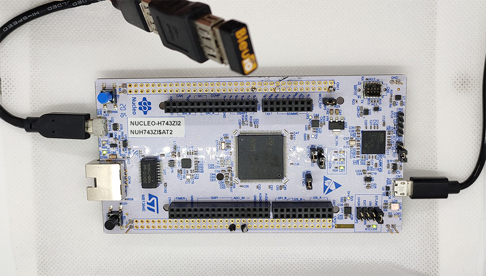
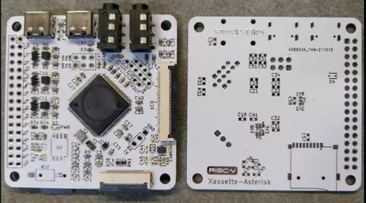
We have used an STM32 Nucleo-144 development board with STM32H743ZI MCU (STM32H743ZI micro mbed-Enabled Development Nucleo-144 series ARM® Cortex®-M7 MCU 32-Bit Embedded Evaluation Board) for this example.

If you want to use another setup you will have to make sure it supports USB Host and beware that the GPIO setup might be different and may need to be reconfigured in the .ioc file.

2. About the Code

You can get the project HERE

https://github.com/smart-sensor-devices-ab/stm32_bleuio_example

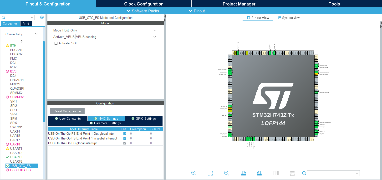
This project-based on a new STM32 project with these changes in the .ioc file:

Under ‘Connectivity’ the ‘USB_OTG_FS’-mode is changed to Host_Only and in the NVIC Settings all global interrupts are enabled

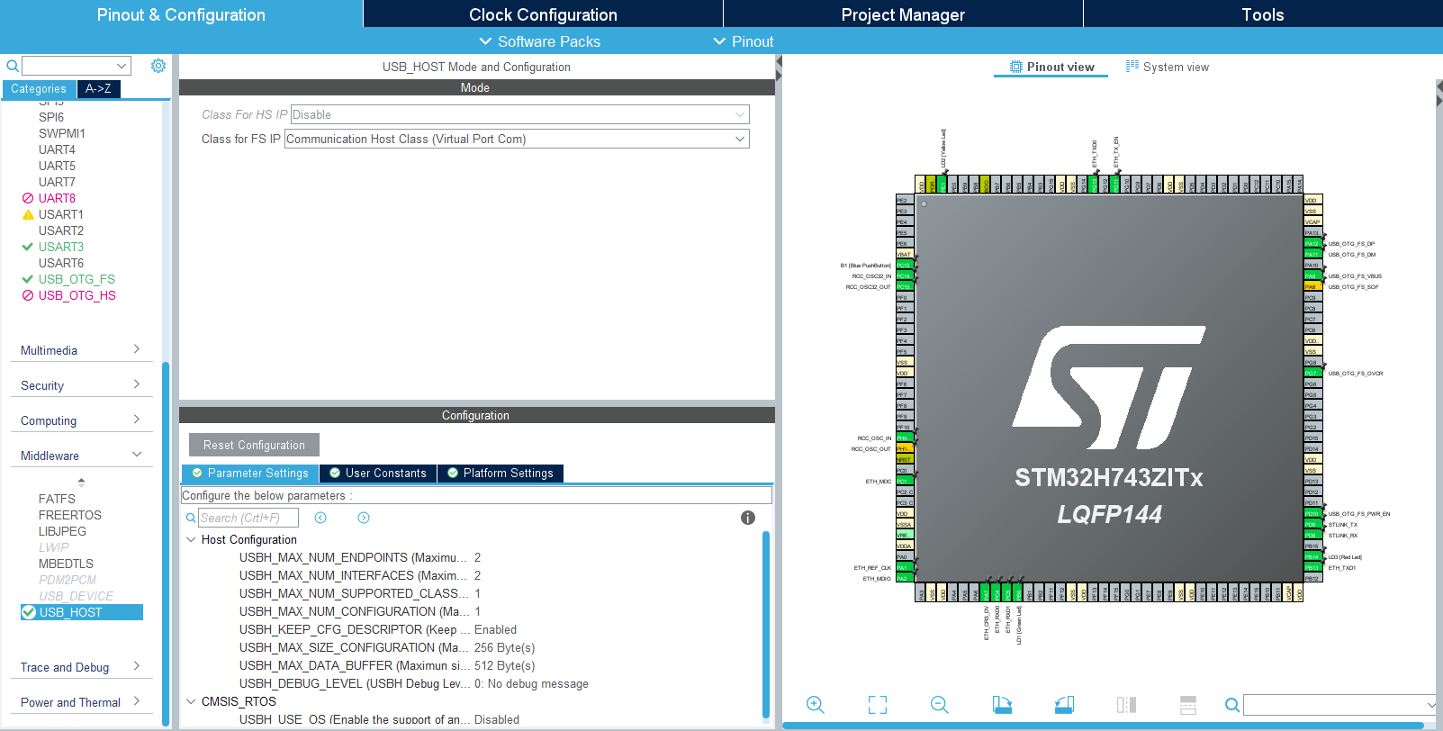
And under ‘Middleware’ the ‘USB_HOST’- ‘Class for FS IP’ is set to ‘Communication Host Class (Virtual Port Com)’.

To make sure the host would recognize when the bootloader is done and the BleuIO firmware is running this was added in the USBH_UserProcess function in ‘usb_host.c’ (found under ‘USB_HOST’ -> ‘App’ folder):

static void USBH_UserProcess  (USBH_HandleTypeDef *phost, uint8_t id)
{
  /* USER CODE BEGIN CALL_BACK_1 */
  switch(id)
  {
  case HOST_USER_SELECT_CONFIGURATION:
  break;

  case HOST_USER_DISCONNECTION:
  Appli_state = APPLICATION_DISCONNECT;
  isBleuIOReady = false;

  // Turn on Red LED, turn off Green and Yellow LED
  HAL_GPIO_WritePin(GPIOB, GPIO_PIN_0, GPIO_PIN_RESET);
  HAL_GPIO_WritePin(GPIOE, GPIO_PIN_1, GPIO_PIN_RESET);
  HAL_GPIO_WritePin(GPIOB, GPIO_PIN_14, GPIO_PIN_SET);
  break;

  case HOST_USER_CLASS_ACTIVE:
  Appli_state = APPLICATION_READY;
  // Check if BleuIO firmware is running
  // (idProduct:0x6001 = bootloader, idProduct:0x6002 = bleuio fw)
  if(phost->device.DevDesc.idProduct == 0x6002)
  {
      isBleuIOReady = true;
      // Sends message to uart that BleuIO is connected and ready
      HAL_UART_Transmit(&huart3, (uint8_t*)BLEUIO_READY, strlen(BLEUIO_READY), HAL_MAX_DELAY);

      // Turn on Green LED, turn off Yellow and Red LED
      HAL_GPIO_WritePin(GPIOB, GPIO_PIN_0, GPIO_PIN_SET);
      HAL_GPIO_WritePin(GPIOE, GPIO_PIN_1, GPIO_PIN_RESET);
      HAL_GPIO_WritePin(GPIOB, GPIO_PIN_14, GPIO_PIN_RESET);

      // Start receiving from usb
      USBH_CDC_Receive(&hUsbHostFS, CDC_RX_Buffer, RX_BUFF_SIZE);
  }
  break;

  case HOST_USER_CONNECTION:
  Appli_state = APPLICATION_START;
  isBleuIOReady = false;
  // Turn on Yellow LED, turn off Green and Red LED
  HAL_GPIO_WritePin(GPIOB, GPIO_PIN_0, GPIO_PIN_RESET);
  HAL_GPIO_WritePin(GPIOE, GPIO_PIN_1, GPIO_PIN_SET);
  HAL_GPIO_WritePin(GPIOB, GPIO_PIN_14, GPIO_PIN_RESET);
  break;

  default:
  break;
  }
  /* USER CODE END CALL_BACK_1 */
}

The Green, Red and Yellow LEDs on the Nucleo board are also setup to change based on the connection status.

  • Red = Disconnnected
  • Yellow = Connecting
  • Green = Connected

An external variable bool isBleuIOReady is also set so the status of the dongle is accessible from main.c.

Once the BleuIO dongle is confirmed to be connected the USBH_CDC_Receive function is run to start receiving data from the USB CDC.

The USBH_CDC_ReceiveCallback also needs to be implemented:

void USBH_CDC_ReceiveCallback(USBH_HandleTypeDef *phost)
{
    if(phost == &hUsbHostFS)
    {
        // Handles the data recived from the USB CDC host, here just printing it out to UART
        rx_size = USBH_CDC_GetLastReceivedDataSize(phost);
        HAL_UART_Transmit(&huart3, CDC_RX_Buffer, rx_size, HAL_MAX_DELAY);

        // Reset buffer and restart the callback function to receive more data
        memset(CDC_RX_Buffer,0,RX_BUFF_SIZE);
        USBH_CDC_Receive(phost, CDC_RX_Buffer, RX_BUFF_SIZE);
    }

    return;
}

In this example, the received data is just echoed to the UART.

To send data to the Dongle the USBH_CDC_Transmit function is used. In this example, UART input is used to send different commands.

For this purpose, a wrapper function has been created that can be accessed from main.c:

/**
  * @brief Simple function that takes a string and transmit it to the dongle
  * @retval None
  */
void writeToDongle(uint8_t * cmd)
{
    USBH_CDC_Transmit(&hUsbHostFS, cmd, strlen((char *)cmd));
}

In main.c HAL_UART_RxCpltCallback is implemented to receive input from Uart and a simple UART input handler:

void HAL_UART_RxCpltCallback(UART_HandleTypeDef *UartHandle)
{
    if(UartHandle == &huart3)
    {
        RX_value = (int)aRxBuffer[0];
        uartStatus = UART_RX_NONE;

        switch(RX_value)
        {
            case UART_RX_0:
            {
                uartStatus = UART_RX_0;
                break;
            }
            case UART_RX_1:
            {
                uartStatus = UART_RX_1;
                break;
            }
            case UART_RX_2:
            {
                uartStatus = UART_RX_2;
                break;
            }
            default:
            {
                uartStatus = UART_RX_NONE;
                break;
            }
        }
        // Resets uart recieve interrupt mode
        HAL_UART_Receive_IT(&huart3, (uint8_t *)aRxBuffer, RXBUFFERSIZE);
    }
}


/**
  * @brief Simple uart input handler
  * @retval None
  */
void handleUartInput(UARTCommandTypeDef cmd)
{
    switch(cmd)
    {
        case UART_RX_0:
        {
            // 0
            uart_buf_len = sprintf(uart_tx_buf, "\r\n(0 pressed)\r\n");
            HAL_UART_Transmit(&huart3, (uint8_t *)uart_tx_buf, uart_buf_len, HAL_MAX_DELAY);
            if(isBleuIOReady)
            {
                writeToDongle((uint8_t*)DONGLE_CMD_ATI);
            } else
            {
                uart_buf_len = sprintf(uart_tx_buf, BLEUIO_NOT_READY_MSG);
                HAL_UART_Transmit(&huart3, (uint8_t *)uart_tx_buf, uart_buf_len, HAL_MAX_DELAY);
            }
            uartStatus = UART_RX_NONE;
            break;
        }
        case UART_RX_1:
        {
            // 1
            uart_buf_len = sprintf(uart_tx_buf, "\r\n(1 pressed)\r\n");
            HAL_UART_Transmit(&huart3, (uint8_t *)uart_tx_buf, uart_buf_len, HAL_MAX_DELAY);
            if(isBleuIOReady)
            {
                writeToDongle((uint8_t*)DONGLE_CMD_AT_ADVSTART);
            } else
            {
                uart_buf_len = sprintf(uart_tx_buf, BLEUIO_NOT_READY_MSG);
                HAL_UART_Transmit(&huart3, (uint8_t *)uart_tx_buf, uart_buf_len, HAL_MAX_DELAY);
            }
            uartStatus = UART_RX_NONE;
            break;
        }
        case UART_RX_2:
        {
            // 2
            uart_buf_len = sprintf(uart_tx_buf, "\r\n(2 pressed)\r\n");
            HAL_UART_Transmit(&huart3, (uint8_t *)uart_tx_buf, uart_buf_len, HAL_MAX_DELAY);
            if(isBleuIOReady)
            {
                writeToDongle((uint8_t*)DONGLE_CMD_AT_ADVSTOP);
            } else
            {
                uart_buf_len = sprintf(uart_tx_buf, BLEUIO_NOT_READY_MSG);
                HAL_UART_Transmit(&huart3, (uint8_t *)uart_tx_buf, uart_buf_len, HAL_MAX_DELAY);
            }
            uartStatus = UART_RX_NONE;
            break;
        }
        case UART_RX_NONE:
        {
            break;
        }
        default:
        {
            uartStatus = UART_RX_NONE;
            break;
        }
    }
}

The handleUartInput() handles the inputs 0, 1 and 2 and maps each to a certain Dongle commands. The handler is then put inside the main loop.

/* Infinite loop */
  /* USER CODE BEGIN WHILE */
  while (1)
  {
    /* USER CODE END WHILE */
    MX_USB_HOST_Process();
    /* USER CODE BEGIN 3 */
    // Simple handler for uart input
    handleUartInput(uartStatus);
  }
  /* USER CODE END 3 */

3. Using the example project

3.1 What you will need

A board with an STM32 Microcontroller with a USB port. (A Nucleo-144 development board: NUCLEO-H743ZI2, was used developing this example. (https://www.st.com/en/evaluation-tools/nucleo-h743zi.html)

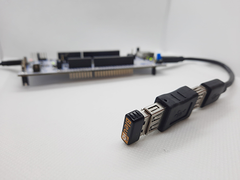
To connect the dongle to the Nucleo board a “USB A to Micro USB B”-cable with a USB A female-to-female adapter can be used.)

4. How to setup project

4.1 Downloading the project from GitHub

Get project HERE

https://github.com/smart-sensor-devices-ab/stm32_bleuio_example

Either clone the project or download it as a zip file and unzip it, into your STM32CubeIDE workspace.

4.2 Importing as an Existing Project

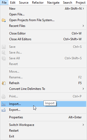
From STM32CubeIDE choose File>Import…

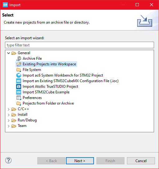
Then choose General>Existing Projects into Workspace then click ‘Next >’

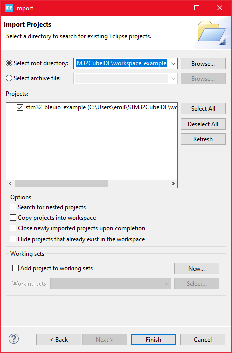
Make sure you’ve choosen your workspace in ‘Select root directory:’

You should see the project “stm32_bleuio_example”, check it and click ‘Finish’.

5. Running the example

  • In STMCubeIDE click the hammer icon to build the project.
  • Open up the ‘STMicroelectronics STLink Viritual COM Port’ with a serial terminal emulation program like TeraTerm, Putty or CoolTerm.Serial port Setup:
    Baudrate: 115200
    Data Bits: 8
    Parity: None
    Stop Bits: 1
    Flow Control: None
  • In STMCubeIDE click the green play button to flash and run it on your board. The first time you click it the ‘Run Configuration’ window will appear. You can just leave it as is and click run.
  • Connect the BleuIO Dongle.
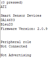
  • Wait until the message: “[BleuIO Dongle Ready]” is shown.

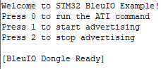
– Press 0 to get device information:

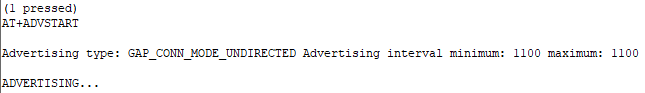
– 1 to start advertising:

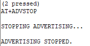
– 2 to stop advertising:

Dongle response will be printed to UART.

SnapEDA Desktop App is now available for Windows

What is the SnapEDA Desktop App?

SnapEDA mission is to help engineers build products faster by removing design barriers.

This is why they created the SnapEDA Desktop App.

It allows our engineers to place parts seamlessly into their CAD tools in a Snap.

DOWNLOAD THE APP

Follow these steps to install the app on Windows:

  1. Extract the downloaded SnapEDA Setup.zip file.
  2. Go to the extracted folder and double-click the SnapEDA Setup.exe to start the installation.
  3. After the installation, you can now use the SnapEDA Desktop App.

Next, find 5 useful articles on how to use this app:

NOTE: They are still optimizing the Mac and Linux versions.

Access BLE data remotely

Suppose you have some BLE devices at your home and want to control or scan for those devices while at your workplace. In this project, we will discuss how to access BLE data remotely.

We have already created a script that communicates through BleuIO dongle remotely and gives us the response. You can access the script at: https://github.com/smart-sensor-devices-ab/bledata_remote_access.git

You are free to clone the script and make changes as you wish.

In this script, JavaScript is used to connect to the dongle using google chrome’s serial port. There is a simple PHP script that helps pass data through the cloud.

Step 1: Uploading

Upload the API folder in any server that supports PHP. This script reads and writes data to a JSON file upon request.

We have uploaded the file at http://smartsensor.io/api/api.php

You can use this URL if you don’t have a server to upload.

Step 2: Home computer setup

Open the index.js file found in the root folder and update the URL of the API file on both occasions.

You can leave the url as it is if you want to use file from our server.

Now connect a BleuIO dongle to your home computer and open the index.html file from the root folder.

Click connect and select the COM port where the dongle is connected.

Step 3: Office / Workplace / remote computer setup

Open the index.html file found in the user folder and update the URL of the API file on both occasions.

You can leave the url as it is if you want to use file from our server.

Now open this file in a browser and start writing AT commands.

Currently, You can access the following AT commands

  • ATI (Returns firmware version, hardware type and unique organization identifier, device connection status )
  • AT+CENTRAL (Sets the device Bluetooth role to central role.)
  • AT+PERIPHERAL (Sets the device Bluetooth role to the peripheral.)
  • AT+DUAL (Sets the device Bluetooth role to dual role. Which means it has both Central and Peripheral role capabilities.)
  • AT+ADVSTART (Starts advertising)
  • AT+ADVSTOP (Stops advertising. Returns ERROR if not already advertising)
  • AT+GAPSTATUS (Reports the Bluetooth role)
  • AT+GAPSCAN=2 (Starts a Bluetooth device scan with the timer set in seconds. Make sure to set a timer for the scan.)

Once you type one of the above commands, you will start to see the response from the dongle on your browser screen.

I am trying to scan for BLE devices at my home where BleuIO dongle is connected. Here I got a list of devices showing on my browser screen. Make sure the device is on central mode to scan for devices.

You can add more AT commands to the script as required. All you need to do is update the index.js file found in the root folder.

Find the list of AT commands our from getting started guide at: https://www.bleuio.com/getting_started/docs/commands/

COM-TGUC6: Compact Solution with 11th Generation Intel® Core™ Processors

AAEON, a leader in embedded computing solutions, announces the COM-TGUC6, their latest COM Type 6 board, featuring the 11th Generation Intel® Core™ processor. The COM-TGUC6 offers developers and users a significant increase in performance over previous generations of COM boards, with faster memory speeds, greater display support, and higher bandwidth connections. The COM-TGUC6 also delivers a rugged design to work wherever it’s needed.

The COM-TGUC6 brings greater processing performance to embedded computing than before. Along with the 11th Generation Intel Core U processors (formerly Tiger Lake), the COM-TGUC6 delivers faster memory, supporting dual DDR4 modules up to 3200 MHz. The COM-TGUC6 supports in-band ECC, providing memory error detection even with non-ECC memory modules. Together this offers faster, more accurate data processing, vital for increasingly complex applications in robotics and AI computing. Additionally, the COM-TGUC6 can be configured with the industrial grade Intel Core U SKUs, enabling the board to meet WiTAS II wide temperature specifications, providing operation in temperatures from -40°C up to 85°C.

Features

  • 11th Generation Intel® Core™ Processor Family (formerly Tiger Lake UP3)
  • 2 x SODIMM DDR4 3200MHz Memory, up to 32GB (in-band ECC)
  • Intel I225LM Gigabit Ethernet x 1
  • VGA, 18/24-bit 2ch LVDS/eDP, DDI x 3
  • High Definition Audio Interface
  • SATA3.0 x 2
  • USB 2.0 x 8, USB 3.2/2.0 x 4 (up to USB 3.2 Gen 2 support)
  • PCI-Express [x1] x 5 (Gen3), PEG [x4] x1 (Gen4)
  • 12V DC input
  • COM Express Type 6, Compact size, 95mm x 95mm

The COM-TGUC6 is designed to bring faster data processing and connections, utilizing the latest generation of I/O and expansion features. One key feature is the Intel® i225LM chipset, powering 2.5 Gbps Ethernet speeds. This enables faster network connections for applications that demand higher bandwidths. Additionally, the system supports four USB3.2 Gen 2 ports, up to eight USB2.0 ports, as well as SATA III storage devices.

The COM-TGUC6 also provides flexible display support, with connections for VGA, up to three DDI ports, and LVDS/eDP support. The board is capable of powering up to four independent displays, perfect for digital signage, medical equipment and gaming. The COM-TGUC6 also supports a range of expansion options including five PCIe Gen 3 lanes, as well as PCI Express Graphics (PEG) Gen 4 [x4].

AAEON provides customers and clients with a range of services to help ensure the right product for the job. From carrier boards and enclosures to OEM/ODM services, AAEON’s industry-leading service and support helps accelerate development and reduce time to market.

more information: https://www.aaeon.com/en/p/com-express-cpu-modules-com-tguc6

Xassette-Asterisk RISC-V 64 SBC Features Allwinner’s latest D1s SoC and Sells for Less Than $10

Open-source embedded system framework has made processor and SBC innovation more fun and easy, offering many configurable architecture implementations. The RISC-V ISA based hardware, though not very economical, is still very much celebrated even after more than a decade of its existence. So far, we have seen it in a number of devices including the Allwinner D1 based Nezha RISC-V Linux SBC currently sold for a little over $100, and the SdtElectronics’s Xassette-Asterisk, an evaluation board based on Allwinner’s latest D1s SoC coming out for under $10.

Xassette-Asterisk SBC features Allwinner’s single-core RISC-V 64 SoC, F133/D1s, which runs at 1.008GHz with an inbuilt 64MB DDR2, and an operating input voltage of 5V supplied via a USB-C port or 3.3V via pin header. The SBC also features digital and analog interfaces including USB ports, micro-SD slot, LCD connector, and headphone interface in a compact 56×56 mm – 2 layer board. According to SdtElectronics, the SBC has been tested with an 800×480 parallel LCD even though the F133 manual reveals support for up to 1920×1080 parallel LCD. The board, however, does not feature GMAC and WiFi modules, which the designer claims are to reduce complexity and cost, but it still supports easy internet access. SdtElectronics also claims that networks can be shared with a computer via RNDIS Gadget, a USB Ethernet support protocol of Linux-Sunix.

Key Features and Specifications of the board:

  • 1.008 GHz, 64MB DDR2, Allwinner D1s single-core 64-bit RISC-V chip
  • MicroSD card slot, 32 MBit SPI flash
  • 40-pin LCD interface, 6-pin touch panel interface, backlight power
  • 24-pin MIPI CSI interface
  • Headphone with mic jack (3.5mm), Line-in jack (3.5mm)
  • 1x USB Type-C OTG port
  • 1x USB Type-C host port (1)
  • 34-pin GPIO header with SPI, I2C, UART, PWM, DAC, ADC, IR Tx, R, power (5V, 3.3V, and GND)
  • 3-pin UART header (serial console usable)
  • Reset button
  • Power Supply:
    • 5V via USB-C port
    • 3.3V via pin header (Not supported by USB due to absence of 5V)
  • Dimension: 56mm x 56mm

The Xassette-Asterisk is an open-source hardware product based on the Linux OpenWrt framework. The project’s log added a few days ago claims that D1s only boots the Tina Linux with limited functionality. So, the root directory of the Linux system had been modified to run the Ubuntu filesystem. SdtElectronics also claims that the package manager alongside Internet access supports high software packages. Documentary on PCB and schematics is available on the Github repository.

The Xassette-Asterisk is not for commercial purposes, but its progress is logged at Hackaday In case you want to join the project and build your board. You might have to purchase the Allwinner processor from Taobao for about $5.5 too.

Seeed’s $799 Jetson SUB Mini PC Kit Combines Leetop’s A206 carrier board with a Xavier NX Module

Seeed Studio has launched a Jetson SUB Mini PC Kit designed for AI applications. The 130 mm x 120 mm x 50mm combines Xavier NX module with an A206 carrier board from Leetop.

The Jetson Xavier NX module delivers up to 21 TOPS and with 384 NVIDIA CUDA cores, 48 Tensor cores, Hexa-core Carmel 64-bit ARM CPUs, and two NVIDIA deep learning accelerators engines. The module is also said also offer 8GB LPDDR4x and 8-32GB eMMC 5.1, and preloaded with Nvidia’s Ubuntu-powered Jetpack SDK for tapping it’s AI capabilities.

The Leetop A206 carrier board on the other hand has a number of features including dual MIPI-CSI camera interfaces, a CANBus header, and 40-pin GPIO. The module also has a real-time clock with coin cell socket, a 15V/3A DC input, and a -25 to 80° operating temperature range.

The Jetson SUB mini PC also comes with a case, a heat sink, and a fan. There’s also a 512GB SSD, WiFi and BT, GbE, HDMI, DP, and 4x USB. The kit is ideal for high-performance compute and AI in embedded and edge systems. It is a choice platform for running modern neural networks in parallel and process high-resolution data from multiple sensors simultaneously.

Features and Specifications of the Jetson SUB mini PC include:

  • NVIDIA Jetson Xavier NX module with:
    • 6-core NVIDIA Carmel ARMv8.2 64-bit processor with 6 MB L2 + 4 MB L3 cache
    • NVIDIA Volta architecture with 384 NVIDIA CUDA cores and 48 Tensor cores
    • 2x NVDLA Engines, 7-Way VLIW Vision Processor
    • Multiple 4Kp60 encode, multiple 8Kp30/4Kp30 decode
    • 8 GB 128-bit LPDDR4x 51.2GB/s
    • 10 W | 15 W | 20 W
    • Up to 14 TOPS @ 10 W, Up to 21 TOPS @ 20W
  • 1x MicroSD slot
  • M.2 Key M socket fitted with a 128GB NVMe SSD
  • HDMI and DisplayPort
  • 2x MIPI CSI-2 D-PHY lanes compatible with Raspberry Pi HQ camera and RPi V2 camera
  • Gigabit Ethernet
  • WiFi & Bluetooth via M.2 Key-E card (included)
  • 4x USB 3.1 ports
  • USB 2.0 Micro-B
  • Header with GPIOs, I2C, I2S, SPI, UART
  • Power supply: 9 to 19V DC via power barrel jack
  • Dimensions: 130 mm x 120 mm x 50 mm

The mini PC kit comes with everything needed in terms of hardware and software already installed and set up. It is available for order at $799. Shipping already started on the 5th November this year. You will get it with an acrylic cover, an aluminum frame and two external antennas.

Other useful details on the Jetson SUB Mini PC Kit may be found on Seeed’s Jetson SUB and the A206 carrier board product pages.

STEVAL-L6986IV1 Synchronous Iso-Buck Converter Evaluation Board

STMicroelectronics’ evaluation board with dual isolated output is based on the L6986I

STMicroelectronics’ 38 V, 5 W synchronous iso-buck converter evaluation board generates two isolated voltages (approx. +18 V and between -4 V and -5 V), suitable for supplying IGBT/SiC MOSFET gate drivers or a single isolated voltage using a simple bypass. The board features the L6986I switching converter allowing a fine and adjustable primary output voltage and an isolated secondary output generated using a transformer.

The primary sink capability (typ. 1.9 A) allows appropriate energy transfer to the secondary side and enables a tracked soft-start of the secondary output. The control loop is based on a peak current mode architecture with the device operating in forced PWM. The 300 ns blanking time filters oscillations generated by the transformer leakage inductance and renders the solution more robust.

Pulse-by-pulse current sensing on both power elements implements effective constant current protection on the primary side. At the same time, the secondary output is protected against short-circuit events because of the primary reverse current limit. The secondary voltage is stabilized over current with a power transistor and a shunt voltage reference (TL431).

Features

  • Designed for iso-buck topology
  • 4 V to 38 V operating input voltage
  • Primary output voltage regulation/no optocoupler required
  • 1.9 A typical sink peak primary current capability
  • Peak current mode architecture in forced PWM operation
  • 300 ns blanking time
  • 8 µA IQ-SHTDWN
  • Adjustable fSW and synchronization
  • Embedded primary output voltage supervisor
  • Adjustable soft-start time
  • Internal primary current limiting
  • Overvoltage protection
  • RDS(ON) HS = 180 mΩ, RDS(ON) LS = 150 mΩ
  • Thermal shutdown

more information: https://www.st.com/en/evaluation-tools/steval-l6986iv1.html

LTC3337 Primary Battery State of Health Monitor

Analog Devices Inc. LTC3337 Primary Battery State of Health (SOH) Monitor provides accurate, real-time readings of battery cell discharge, voltage, impedance, and temperature. The LTC3337 is designed to be placed in series with a primary battery with minimal associated series voltage drop. This device integrates an infinite dynamic range coulomb counter that tallies all accumulated battery discharge and stores it in an internal register accessible via an I2C interface. A discharge alarm threshold based on this state of charge (SOC) is programmable. When it is reached, an interrupt is generated at the IRQ pin. Coulomb counter accuracy is constant down to no load.

To accommodate a wide range of primary battery inputs, the peak input current limit of the LTC3337 is pin selectable from 5mA to 100mA.

Coulombs can be calculated for either the BAT_IN or BAT_OUT pin, determined by the AVCC pin connection. A BAL pin is provided for applications utilizing a stack of two supercapacitors (optional) at the output.

The Analog Devices Inc. LTC3337 Primary Battery State of Health Monitor is available in a 12-lead Lead Frame Chip Scale Package (LFCSP) with an exposed pad for improved thermal performance.

Features

  • 8.0V to 5.5V battery input voltage range
  • 100nA quiescent current
  • 8 primary battery peak input current limits
    • 5mA, 10mA, 15mA, 20mA, 25mA, 50mA, 75mA, 100mA
  • SOH monitor for primary battery
    • Integrated coulomb counter (Q)
    • Additional monitors for battery voltage (V), battery impedance (Z), and temperature (T)
  • Integrated ±10mA supercapacitor balancer
  • Primary battery current (BAT_IN) or load current (BAT_OUT) is counted
  • Programmable coulomb counter prescaler for a wide range of battery sizes
  • Programmable discharge alarm threshold with interrupt output
  • I2C interface
  • -40°C to +125°C operating junction temperature range
  • 2mm x 2mm LFCSP-12 package

Block Diagram

Application Circuit

more information: https://www.analog.com/en/products/ltc3337.html

TOP PCB Companies