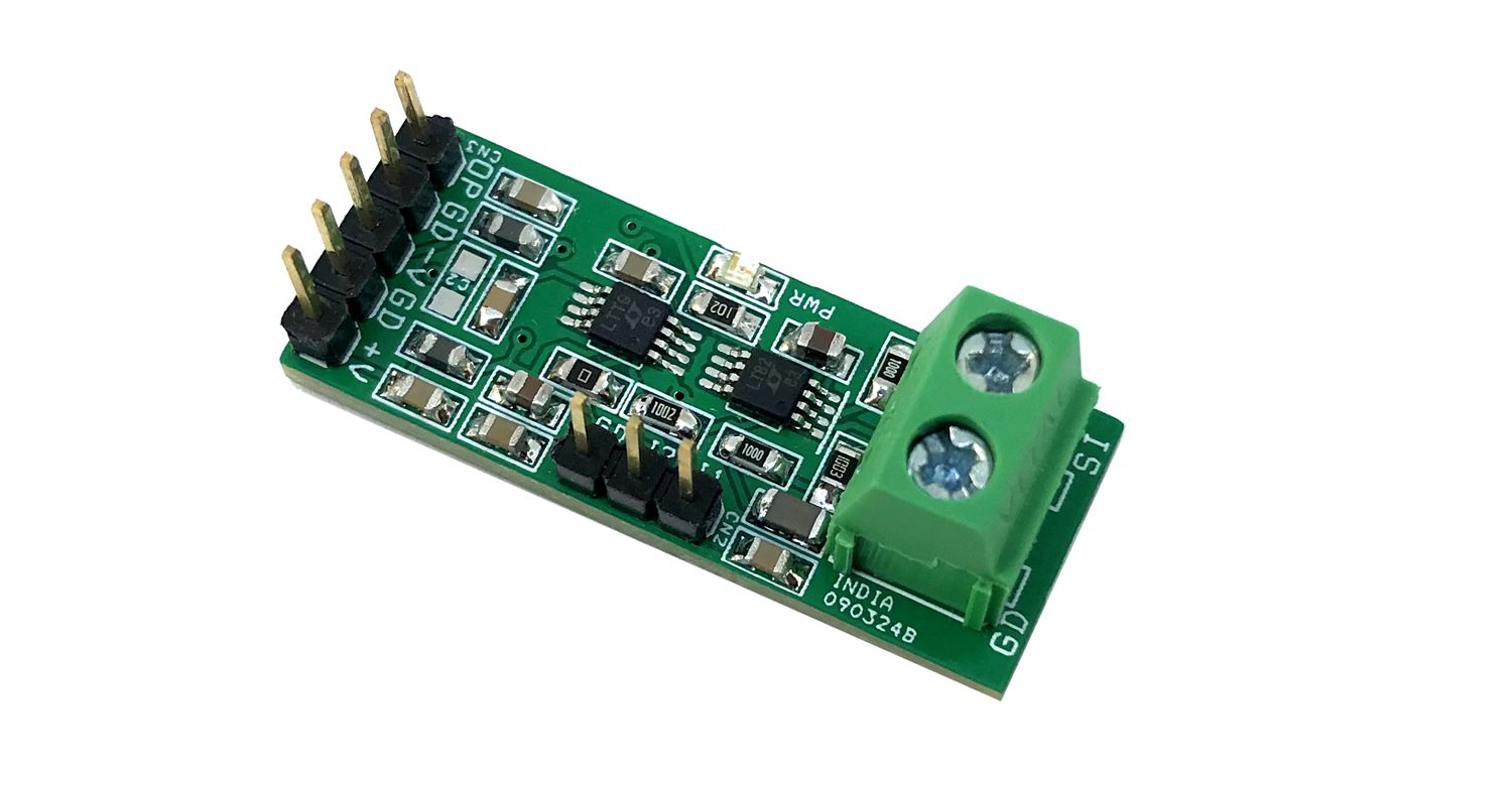
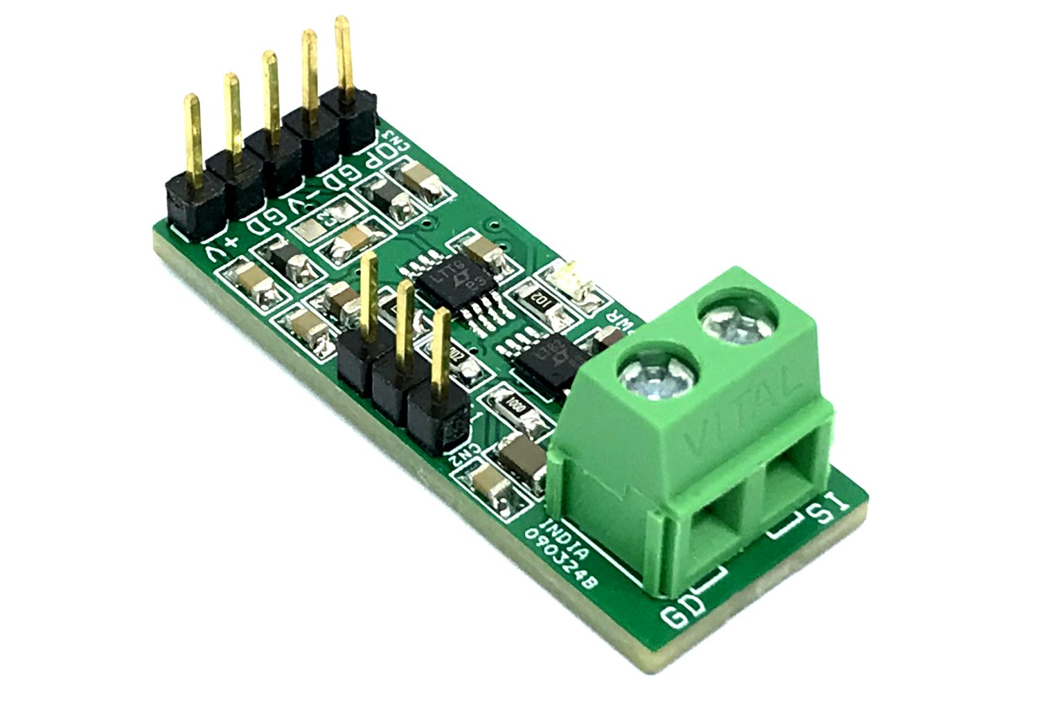
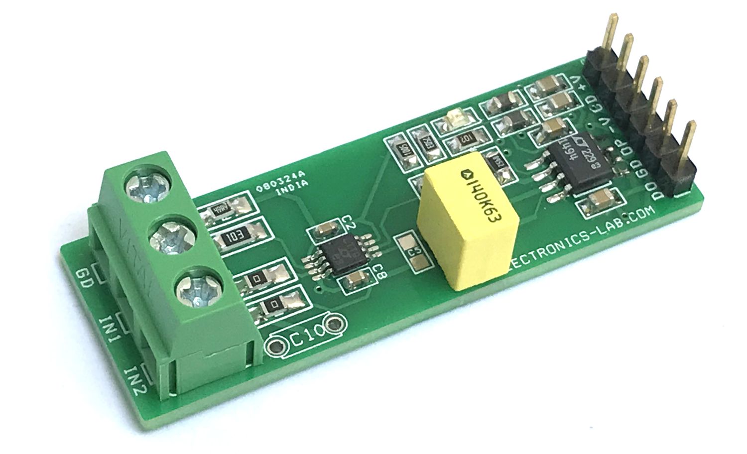
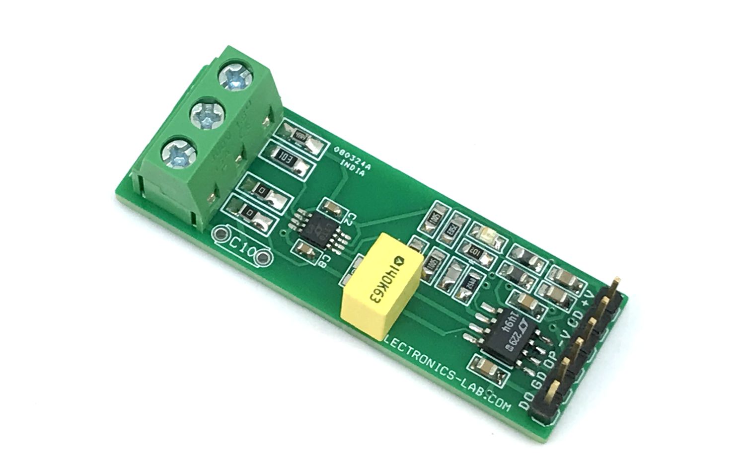
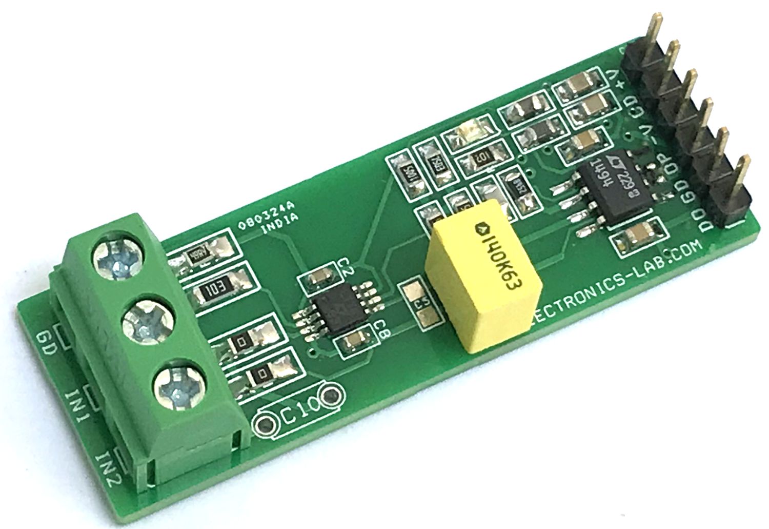
This mini-module helps users to measure the RMS noise of AC signal. Apply the AC noise signal to the input and the circuit outputs a DC voltage. Signal bandwidth is 1Khz to 100Khz and input sensitivity is 1 μVolt RMS. The LT6203 ultra-low noise, low power op-amp amplifies the low-level signal. Further, this signal is converted into a DC voltage by LTC1966 True RMS converter chip from Analog Devices. The circuit works with dual supply +/-5V DC and consumes very low current.
VOutput = 1mVDC/1μVolt RMS Noise
Credits: Schematic is from Analog Devices Application note.
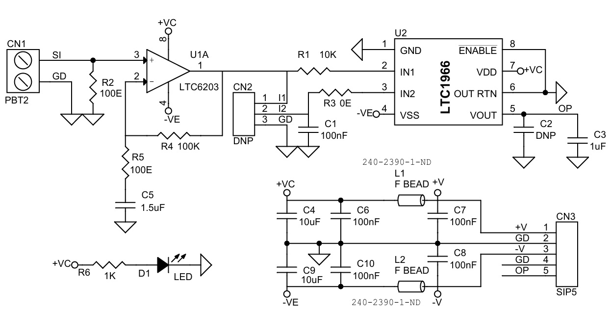
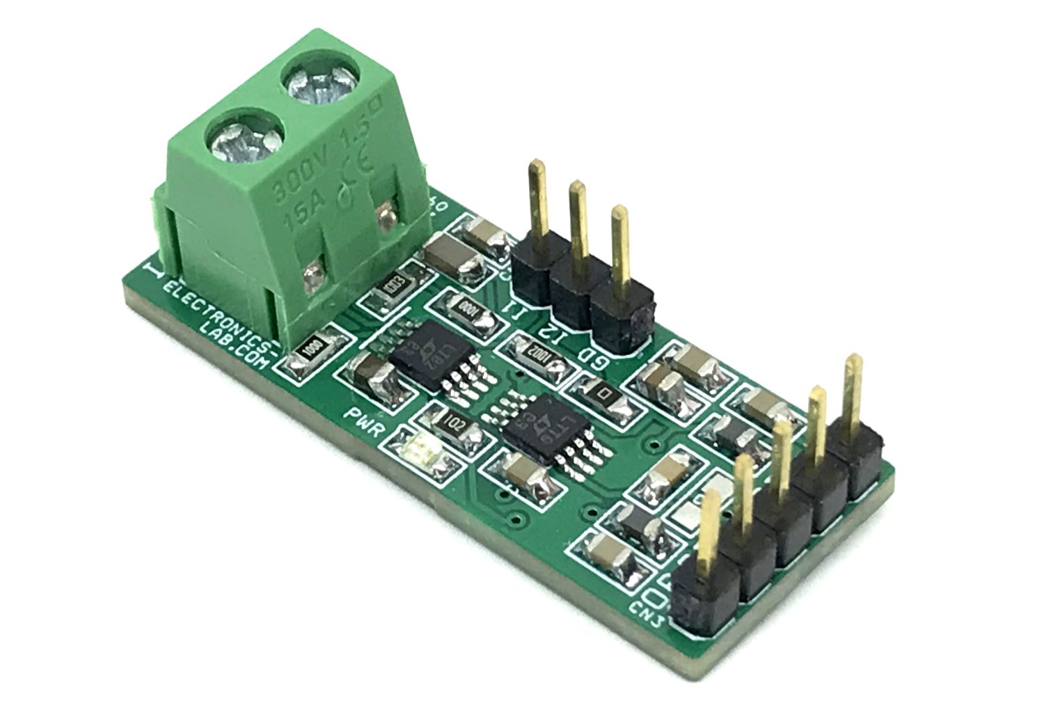
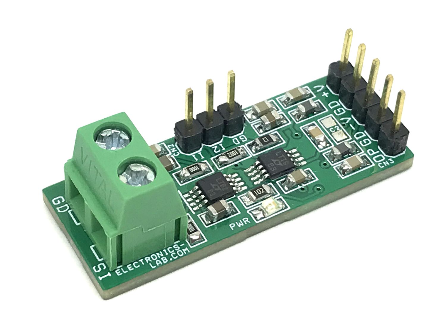
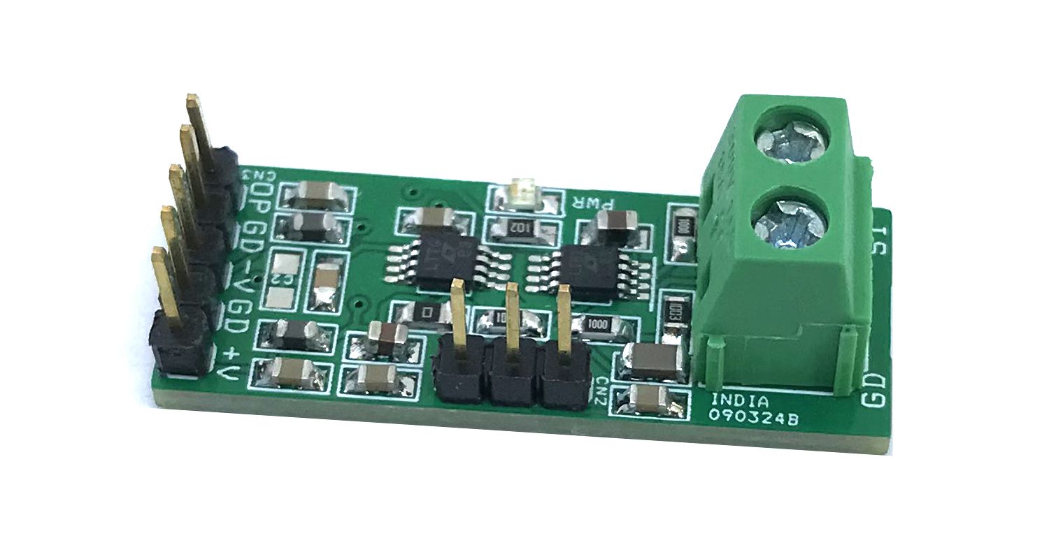
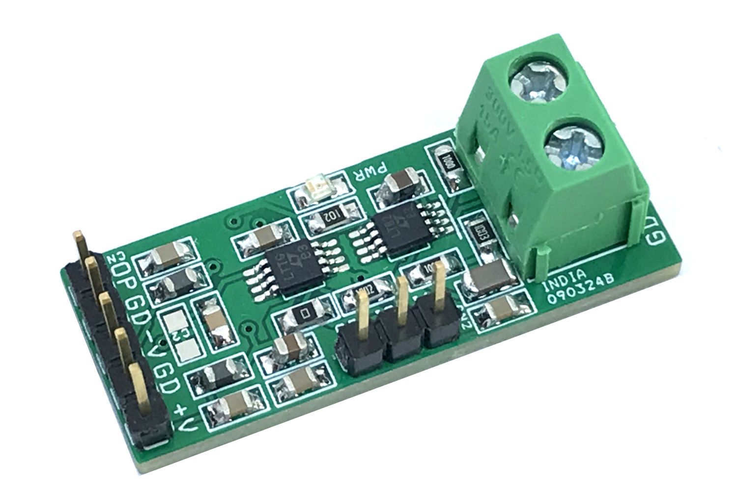
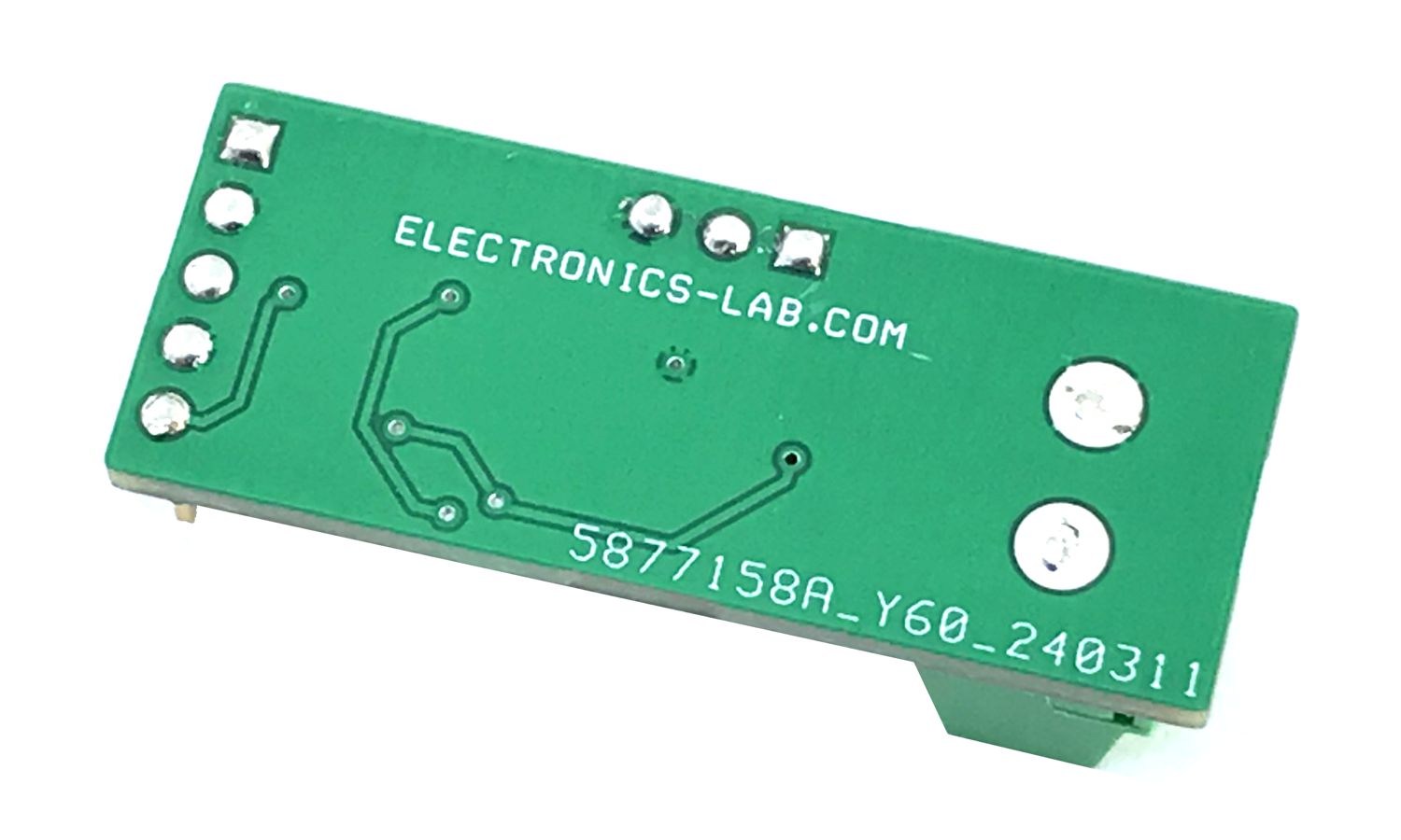
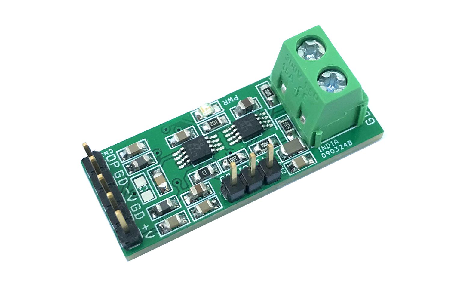
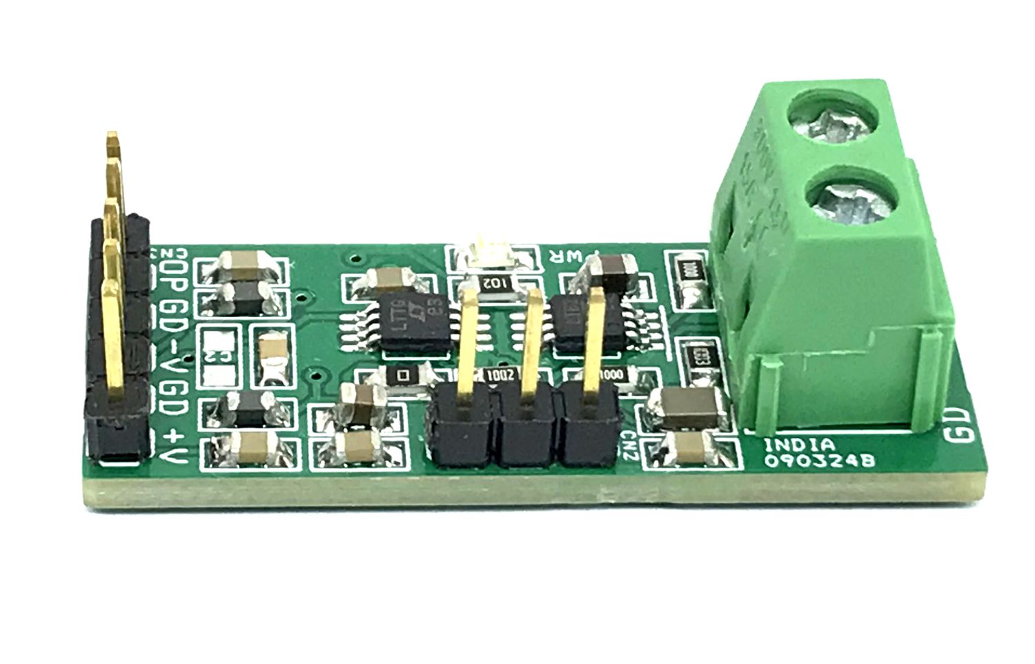
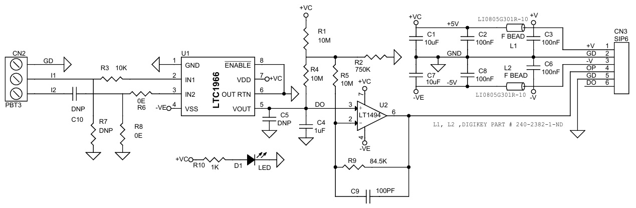
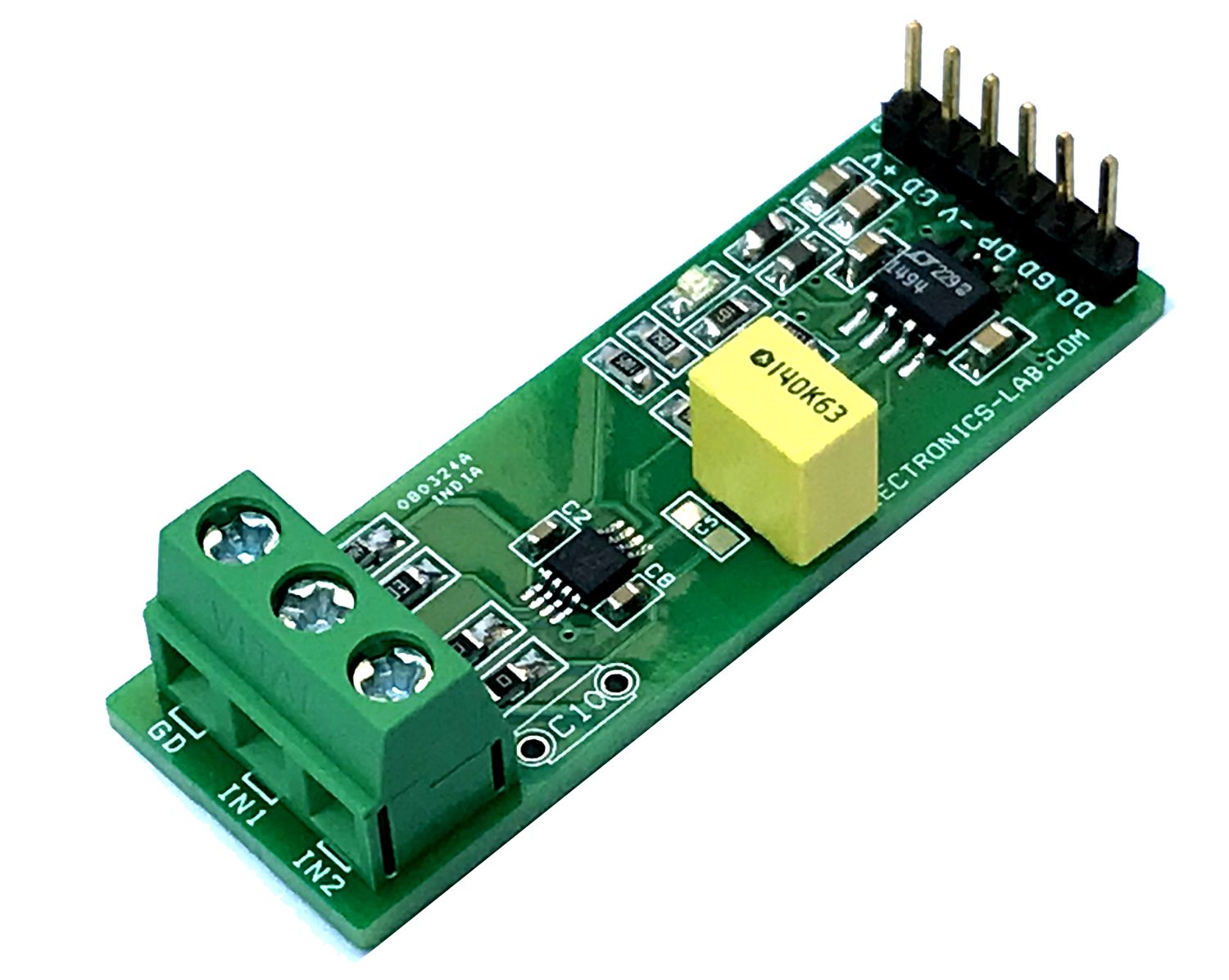
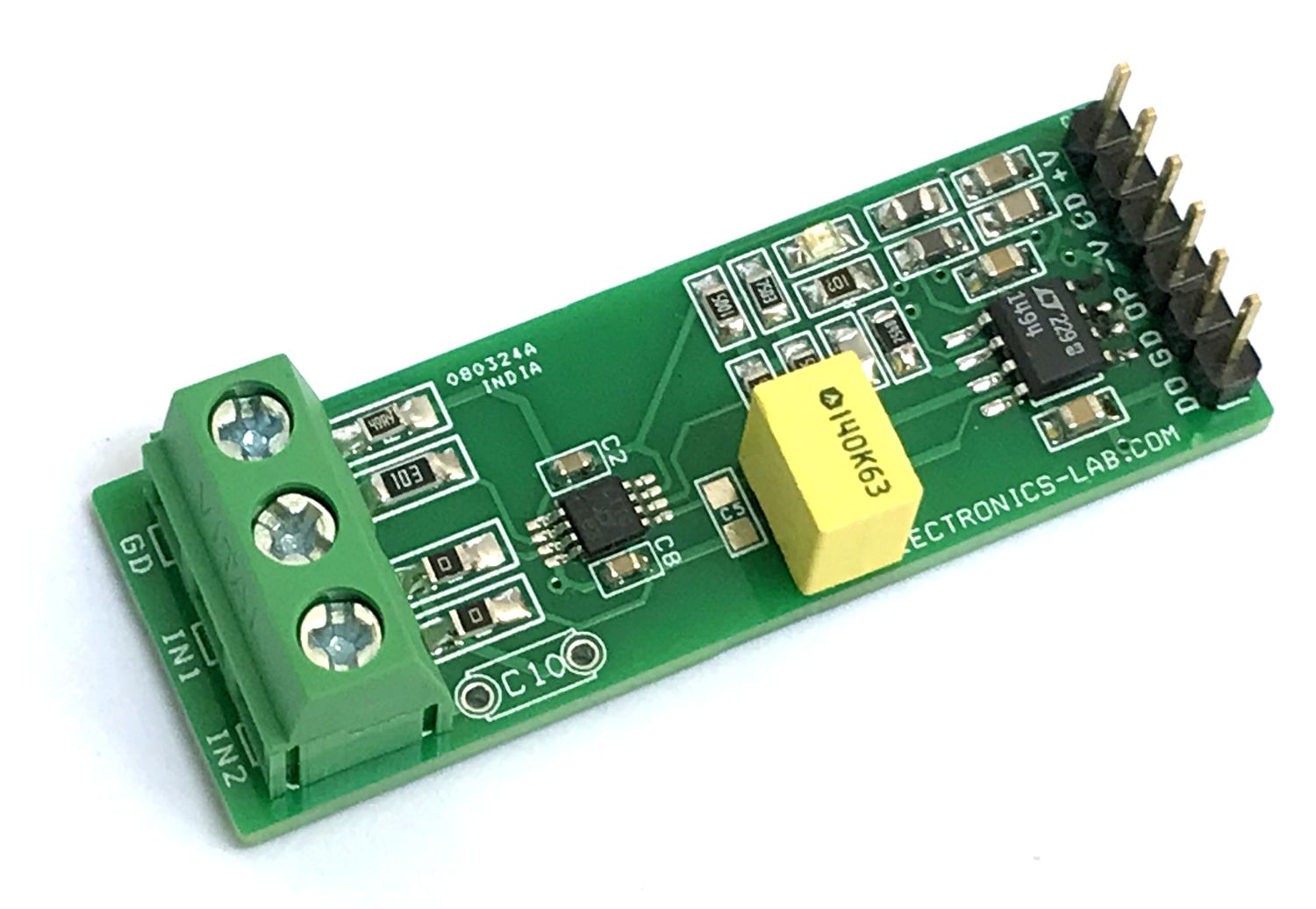
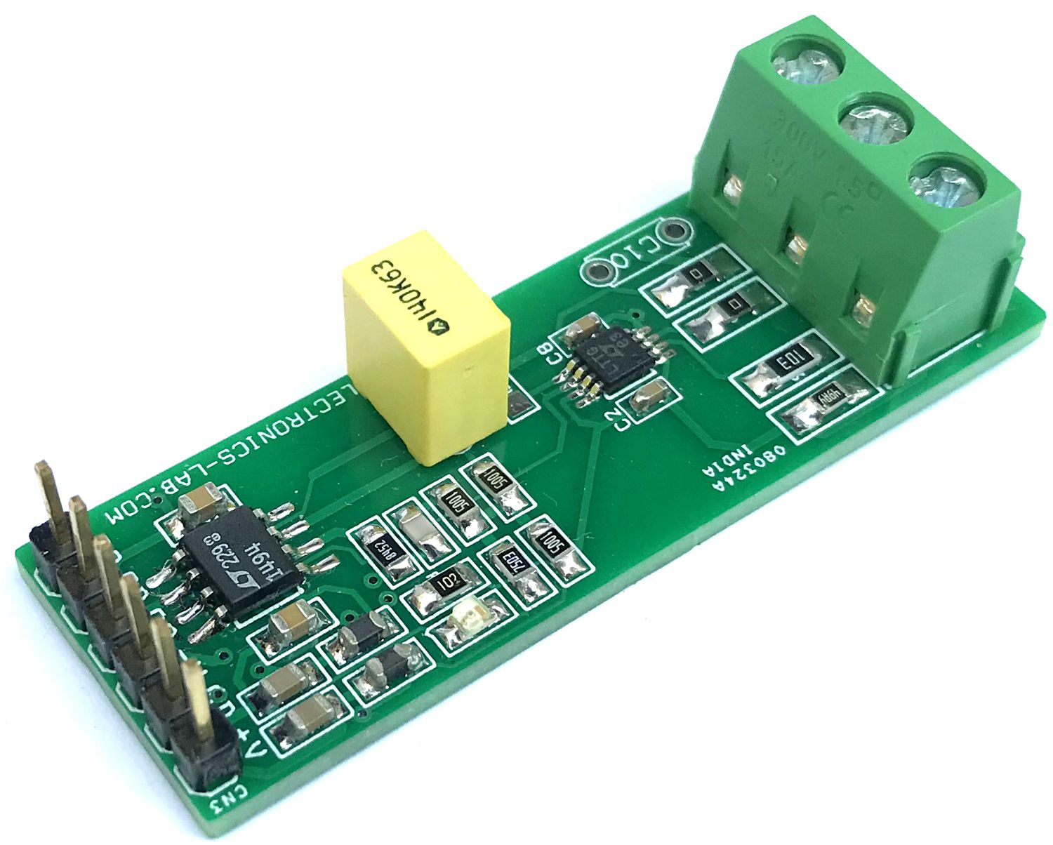
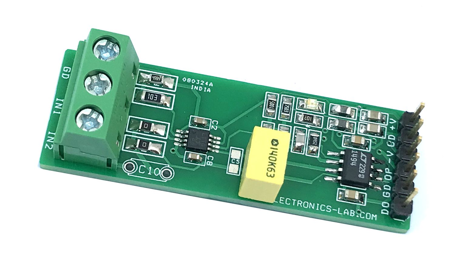
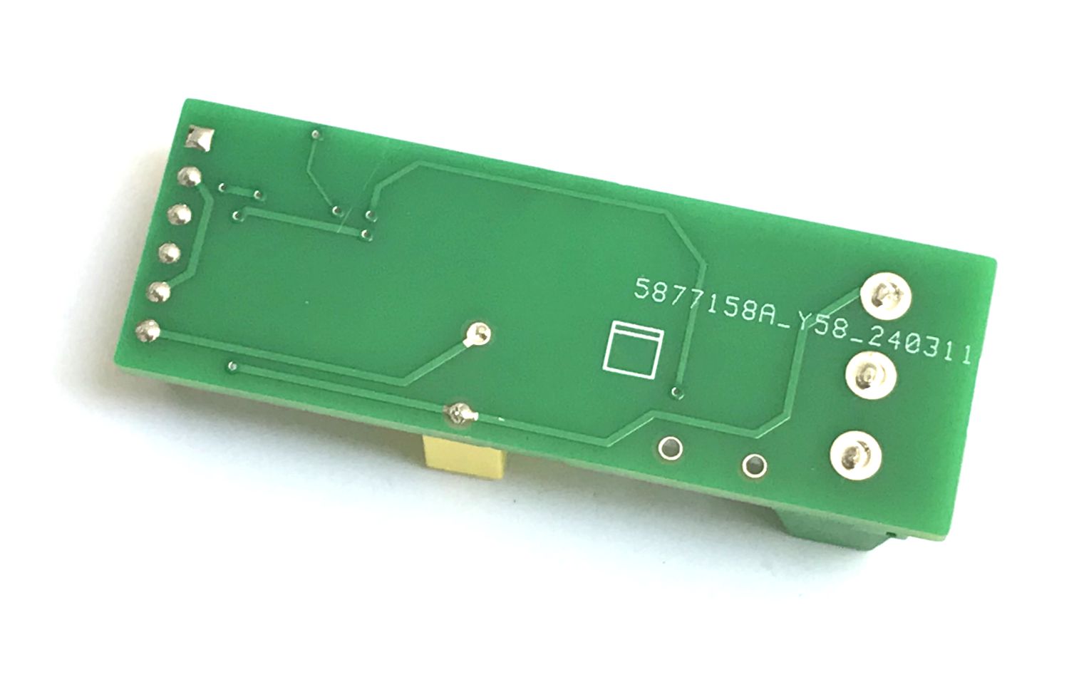
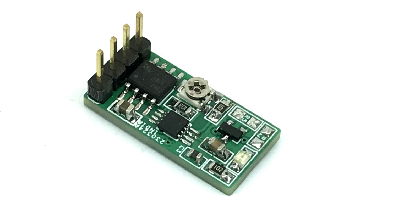
This is a Precision Micro-power true RMS-to-DC converter built using LTC1966 RMS to DC Converter chip and op-amp LTC1494. The RMS to DC that is Converted by LTC1966 and op-amp is used as a post filter to improve AC Response with Offset and Gain Correction. The circuit converts the AC signal into DC. The project works with a single AC input signal and a variety of passive components provided to support configurations for varied applications. Input 1 and Input 2 can be used to feed differential signals. In this case choose appropriate components as per application requirement. Please refer to the datasheet of LTC1966 for more information. The board operates with a dual power supply +/-5V DC. The input voltage range is up to 1V and the output is also up to 1V.
Features
Power Supply ±5.5V (Dual Supply)
True RMS DC Conversion Using ∆Σ Technology
High Accuracy: 0.1% Gain Accuracy from 50Hz to 1kHz, 0.25% Total Error from 50Hz to 1kHz
High Linearity: 0.02% Linearity Allows Simple System Calibration
Constant Bandwidth: Independent of Input Voltage 800kHz –3dB, 6kHz ±1%
Flexible Inputs: Differential or Single-Ended
Up to 1VPEAK Differential Voltage
Output 0 to 1V
Flexible Output: Rail-to-Rail Output
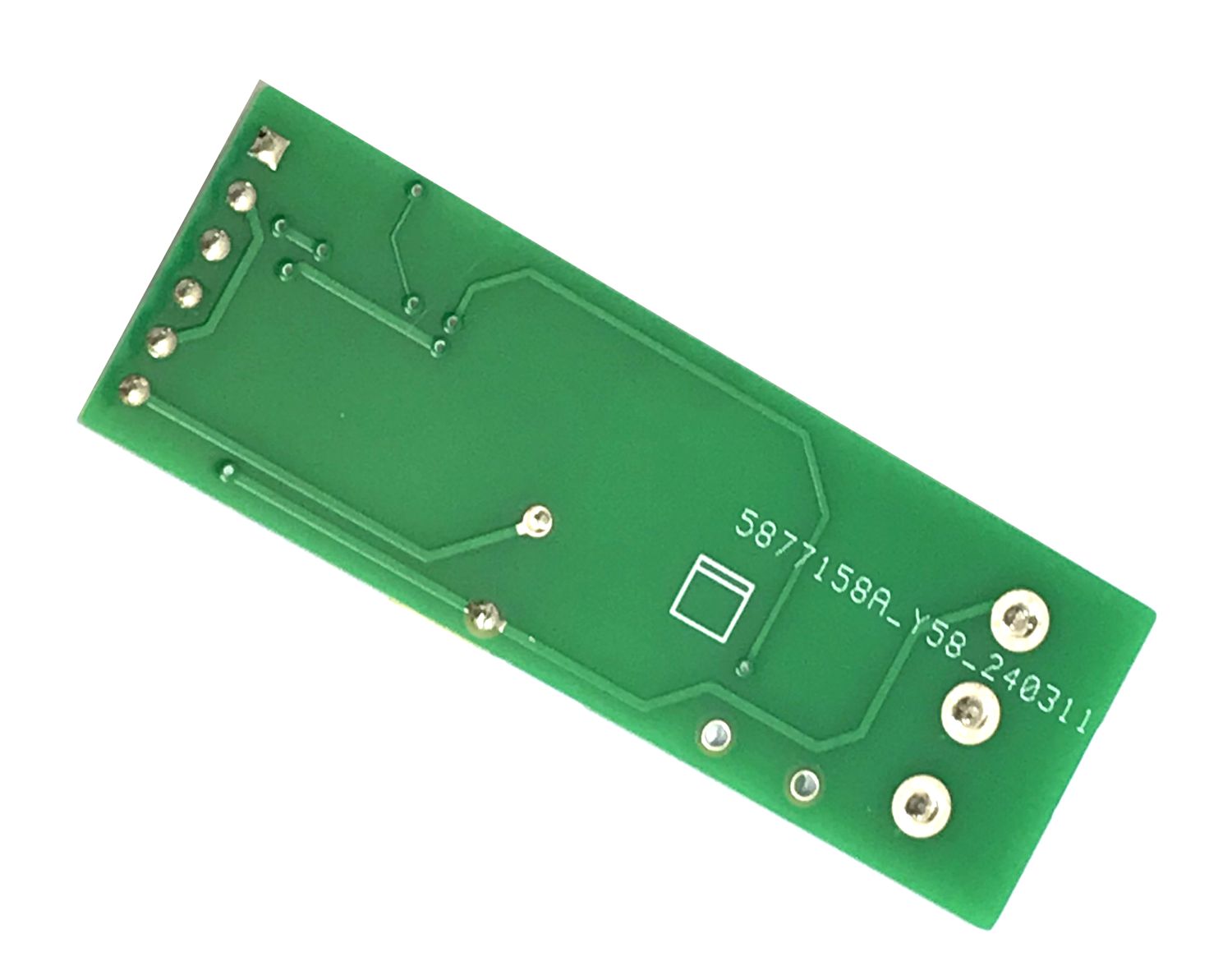
PCB Dimensions 50.80 x 17.78 mm
Applications
True RMS Digital Multi Meters
True RMS Panel Meters
True RMS AC + DC Measurements
Electricity Meters
The LTC1966 is a true RMS-to-DC converter that utilizes an innovative patented ∆Σ computational technique. The internal delta sigma circuitry of the LTC1966 makes it simpler to use, more accurate, lower power and dramatically more flexible than conventional log antilog RMS-to-DC converters. The LTC1966 accepts single-ended or differential input signals (for EMI/RFI rejection) and supports crest factors up to 4. Common mode input range is rail-to-rail. Differential input range is 1VPEAK, and offers unprecedented linearity. Unlike previously available RMS-to-DC converters, the superior linearity of the LTC1966 allows hassle free system calibration at any input voltage. The LTC1966 also has a rail-to-rail output with a separate output reference pin providing flexible level shifting. The LTC1966 operates on a single power supply from 2.7V to 5.5V or dual supplies up to ±5.5V. A low power shutdown mode reduces supply current to 0.5μA.
Circuit shows an analog implementation of this with the offset and gain errors corrected; only the slight, but necessary, degradation in nonlinearity remains. The circuit works by creating approximately 300mV of bias at the junction of the 10MΩ resistors when the LTC1966’s input/output are zero. The 10MΩ resistor to the LTC1966 output therefore feeds in 30nA. The loading of this resistor causes a slight reduction in gain which is corrected, as is the nominal 2.5mV offset, by the LT1494 op amp. The two 10MΩ resistors not connected to the supply can be any value as long as they match and the feed voltage is changed for 30nA injection. The op amp gain is only 1.00845, so the output is dominated by the LTC1966 RMS results, which keeps errors low. With the values shown, the 84.5k resistor is the closest match in the 1% EIA values. This low error sensitivity is important because the LTC1966 output impedance is 85kΩ ±11.8%, which can create a gain error of ±0.1%; enough to degrade the overall gain accuracy somewhat. This gain variation term is increased with lower value feed resistors, and decreased with higher value feed resistors. A bigger error caused by the variation of the LTC1966 output impedance is imperfect cancelation of the output offset introduced by the injected current. The offset correction provided by the LT1494 will be based on a consistent 84.5kΩ times the injected current, while the LTC1966 output impedance will vary enough that the output offset will have a ±300µV range about the nominal 2.5mV. If the two 10MΩ feed resistors to the LT1494 have significant mismatch, cancellation of the 2.5mV offset would be further impacted, so it is probably worth paying an extra penny or so for 1% resistors or even the better temperature stability of thin film devices. The 300mV feed voltage is not particularly critical because it is nominally cancelled, but the offset errors due to these resistance mismatches is scaled by that voltage. Note that the input bias current of the op amp used in circuit is also nominally cancelled, but it will add or subtract to the total current injected into the LTC1966 output. With the 1nA IBIAS of the LT1494 this is negligible. While it is possible to eliminate the feed resistors by using an op amp with a PNP input stage whose IBIAS is 30nA this circuit needs a minimum of 30nA, therefore such an approach may not always work. Because the circuit subtracts the offset created by the injected current, the LT1494 output with zero LTC1966 input will rest at +2.5mV, nominal before offsets, rather than the 5mV.
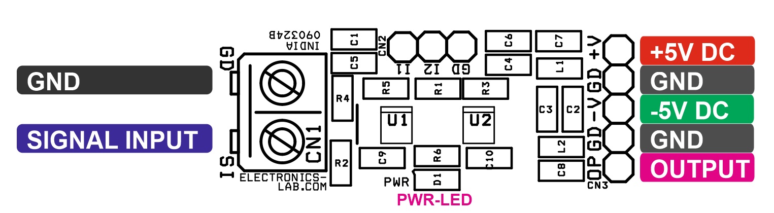
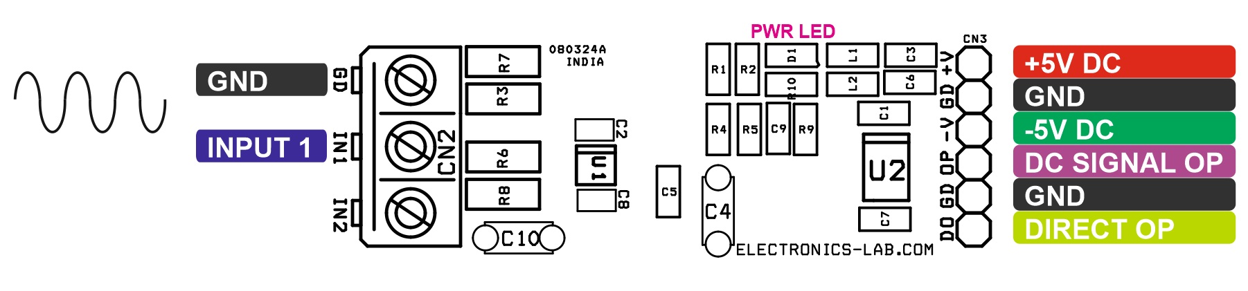
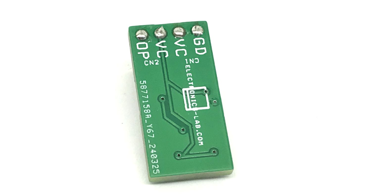
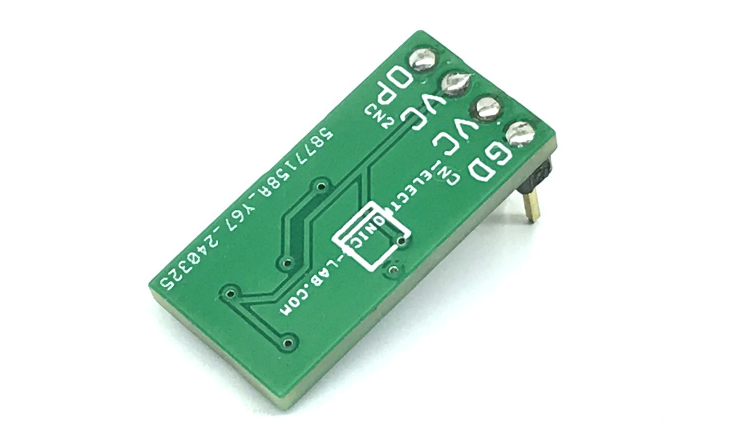
Connections
CN2: Pin1 = GND, Pin 2 = AC Signal Input, Pin 3 = Optional Input 2
CN3: Pin 1 = +V 5V, Pin 2 = GND, Pin 3 = -5V, Pin 4 = DC Signal Output, Pin 5 = GND, Pin 6 = Direct Output from LTC1966
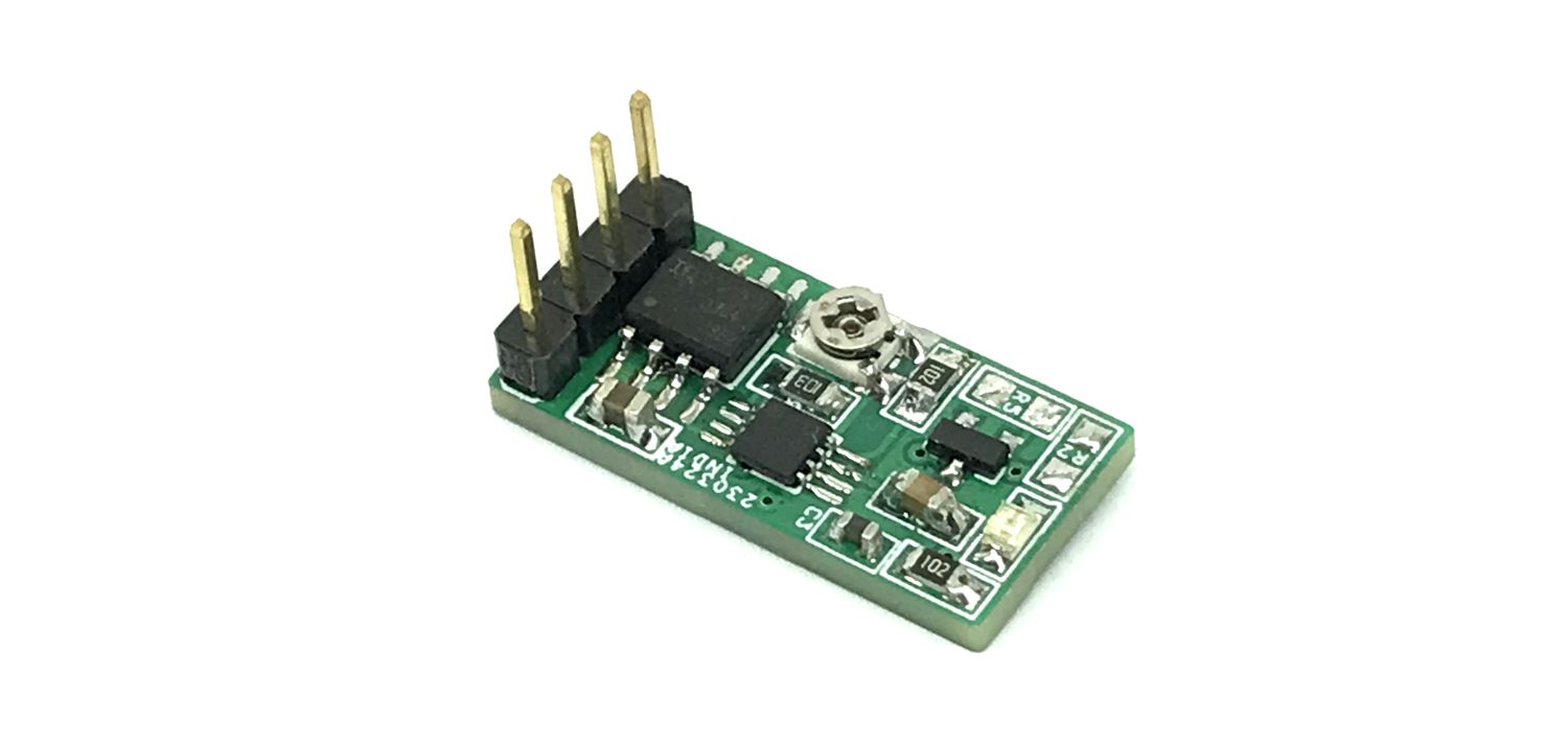
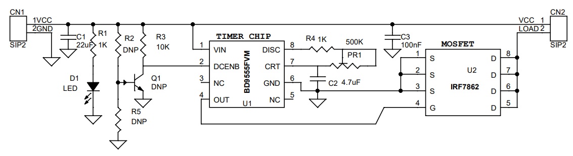
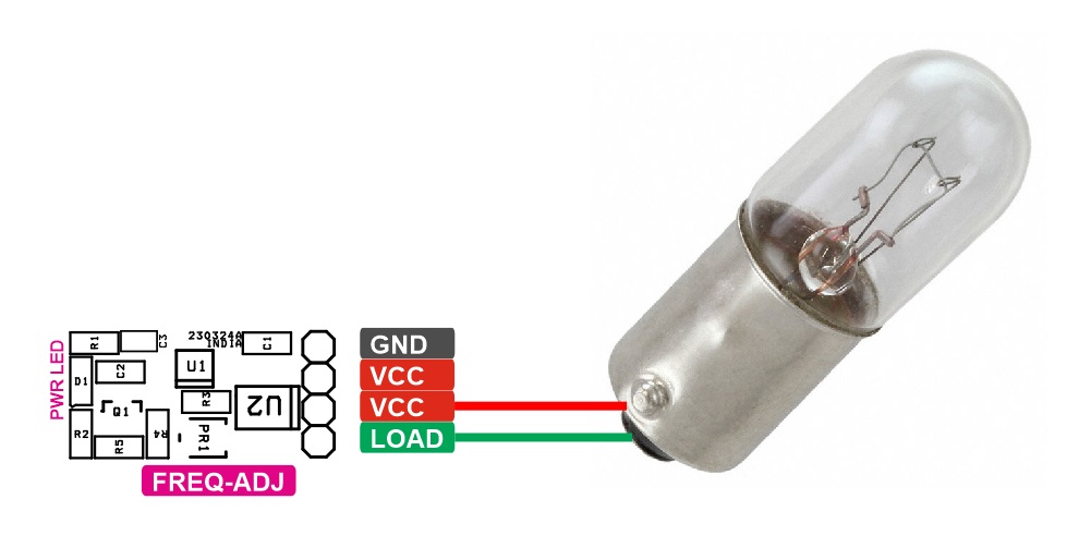
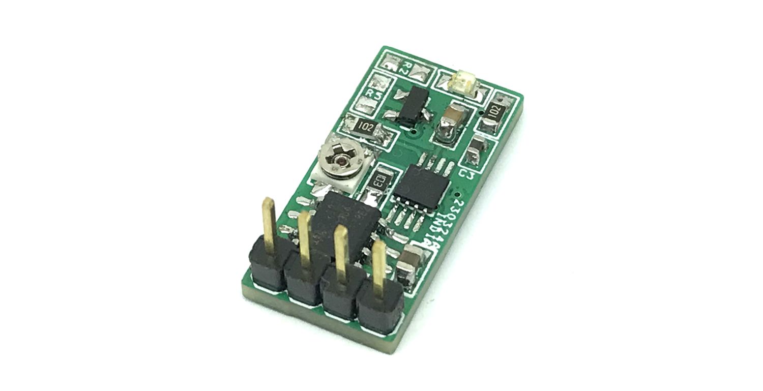
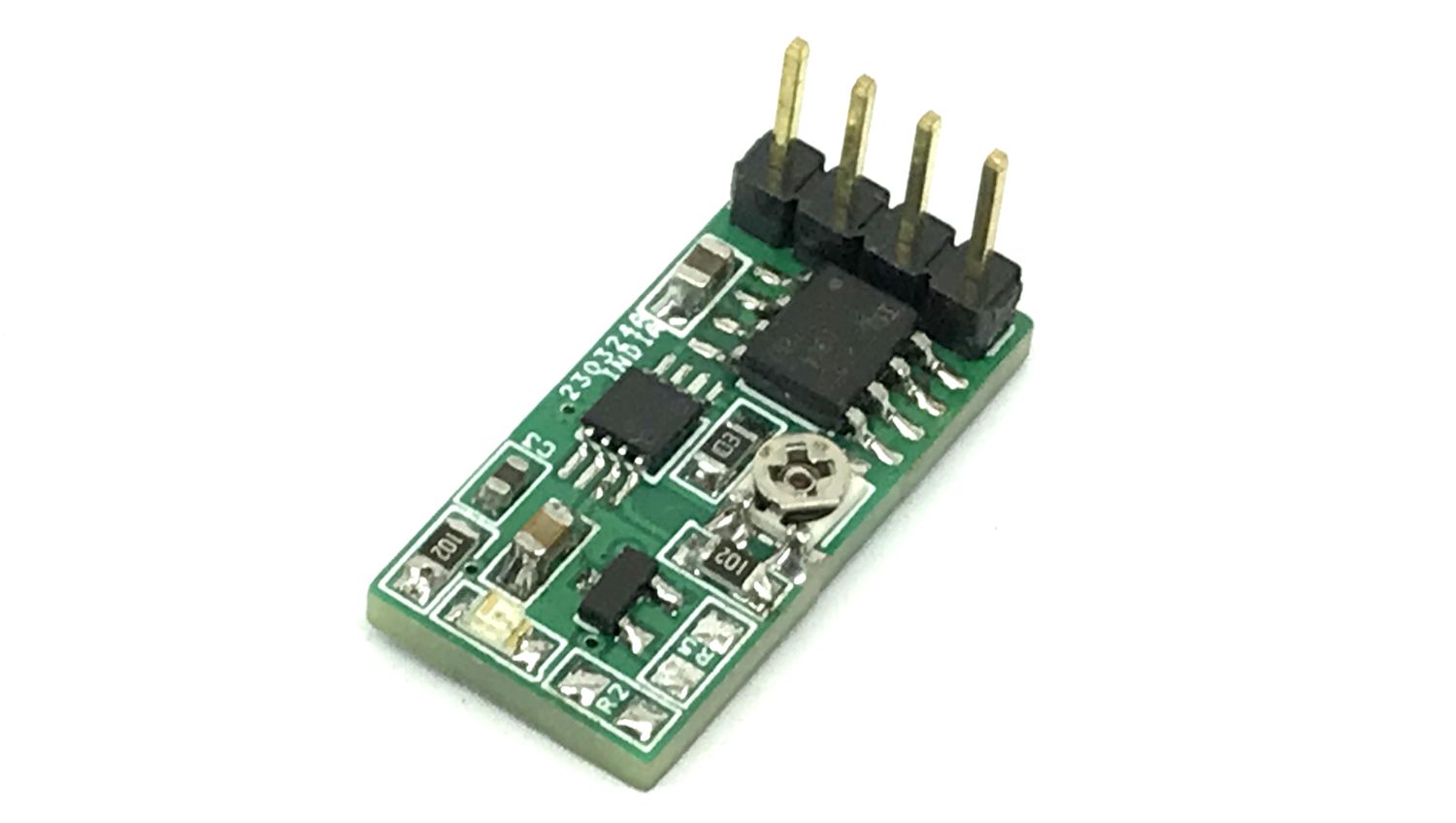
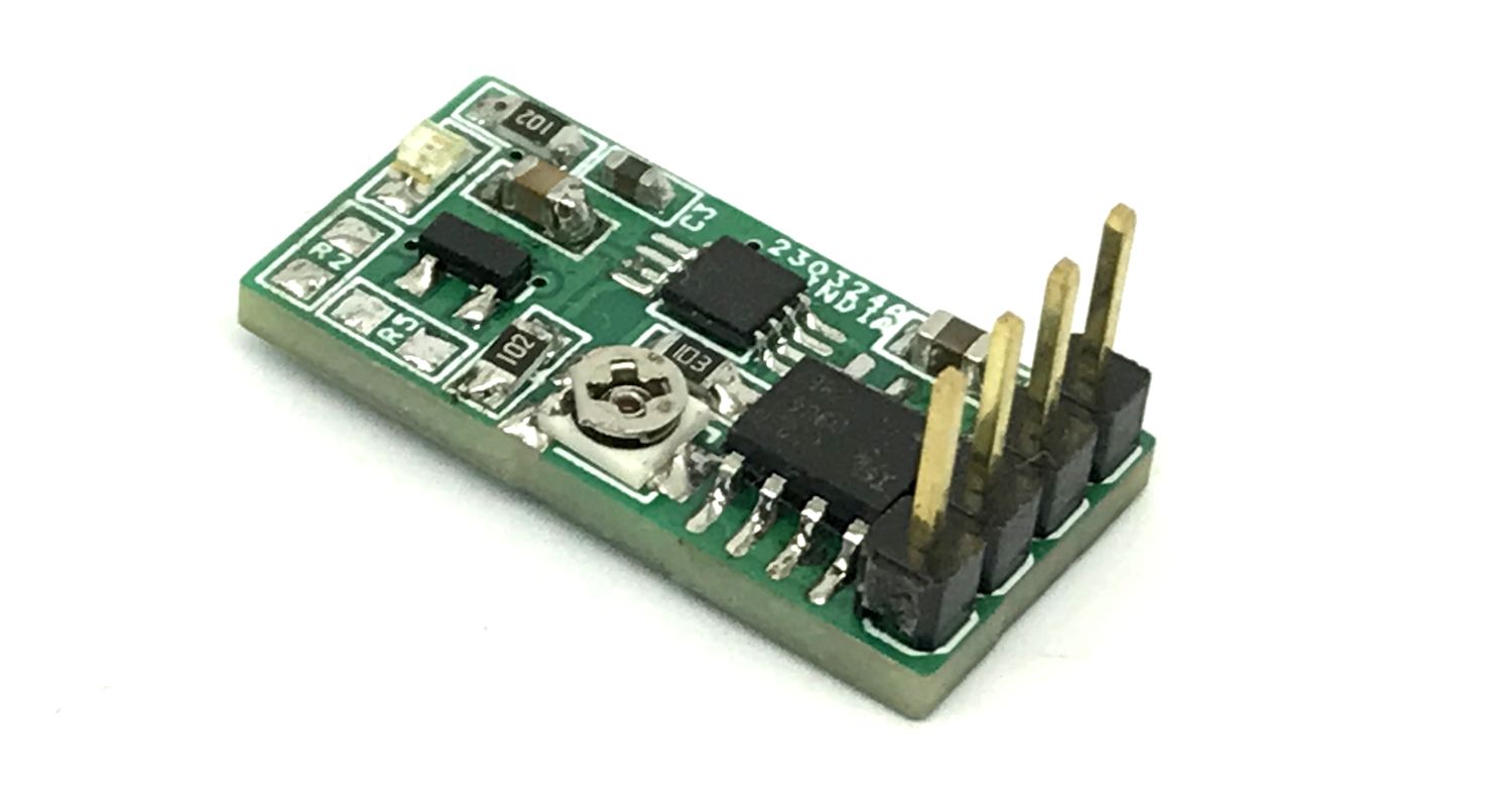
This is a mini flasher board that can drive high-power LED or a lamp, mainly designed for automotive applications. The project consists BD9555FVM-C timer chip and MOSFET. The circuit is configured as a flasher, and can also be used as a PWM driver with an adjustable duty cycle and frequency. Capacitors C2, R4, and PR1 can be used to set the duty cycle. Please refer to the datasheet of BD9555FVM for more information. N-channel IRF7862 MOSFET used to drive the load, and it’s advisable to use maximum load current 3A due to small thermal dissipation on PCB for the MOSFET. The operating power supply is 5V to 15VDC.
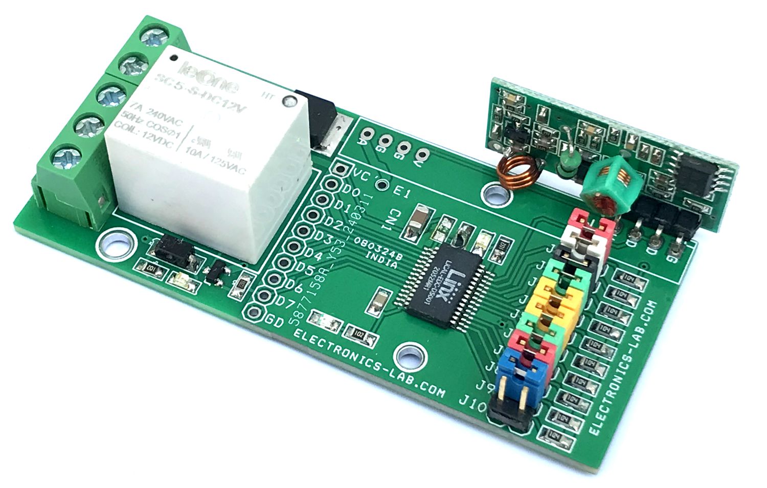
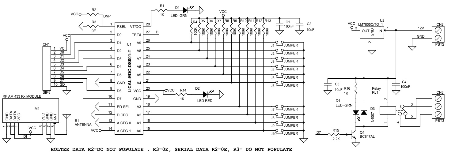
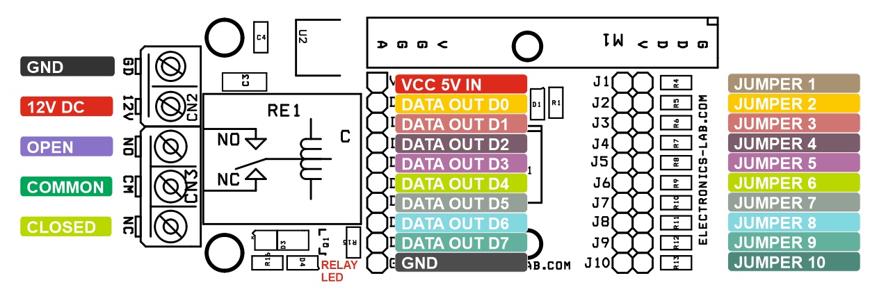
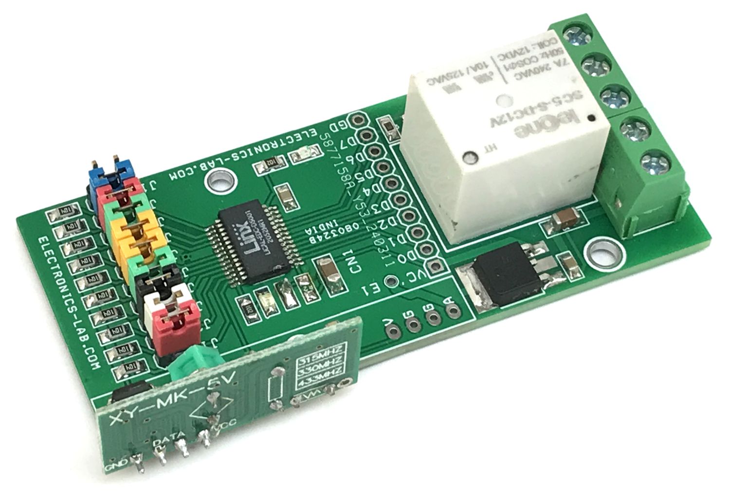
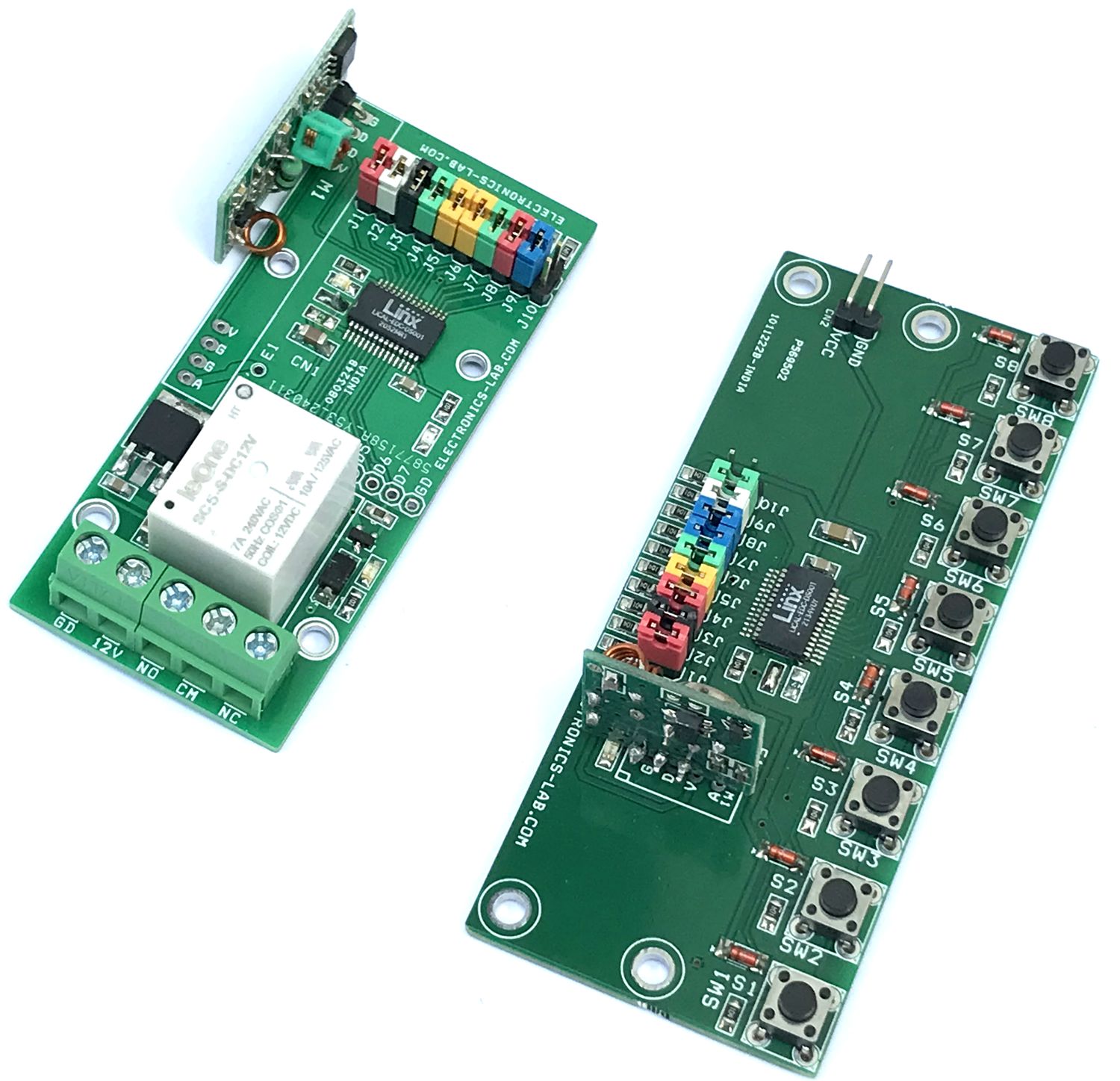
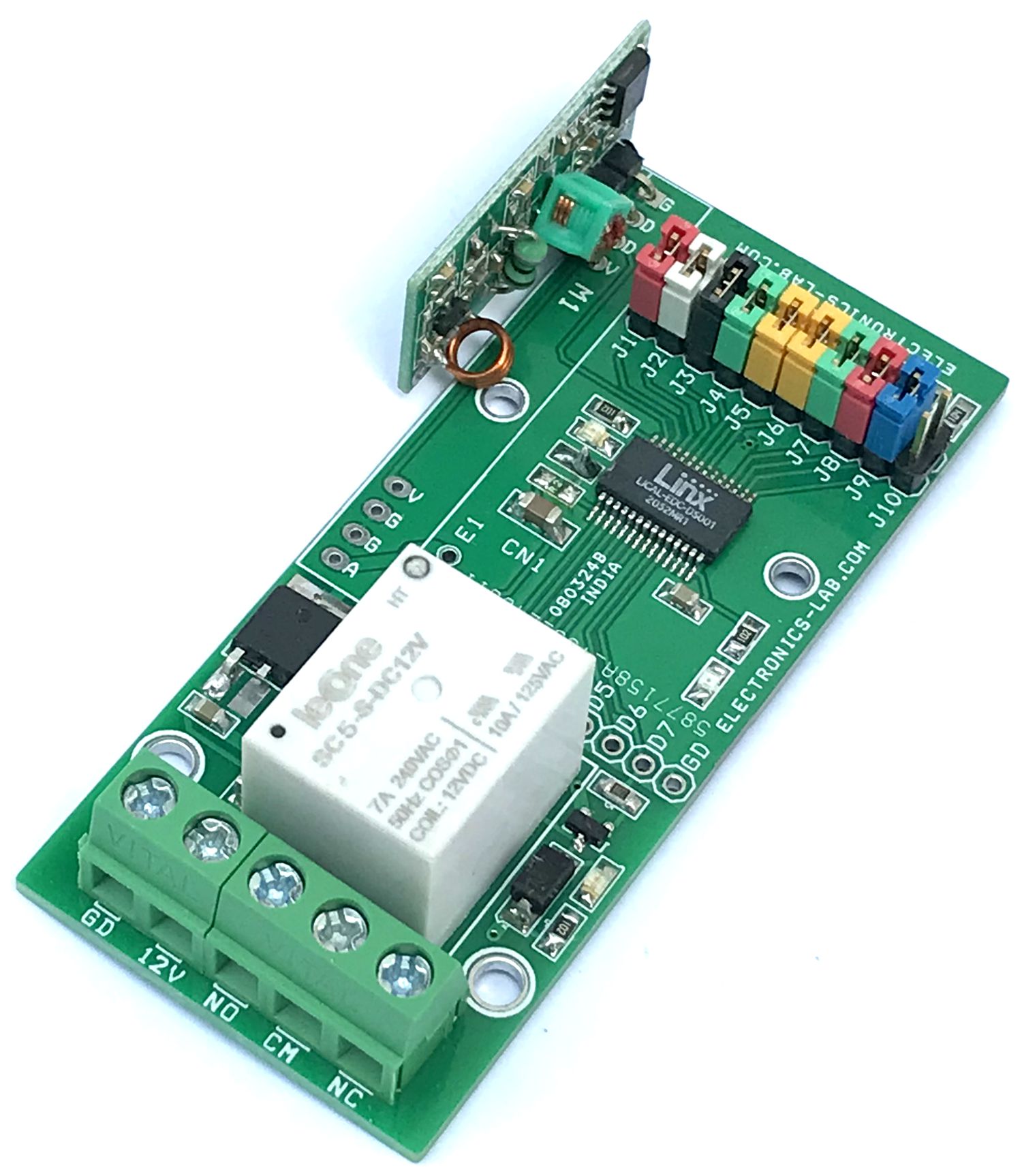
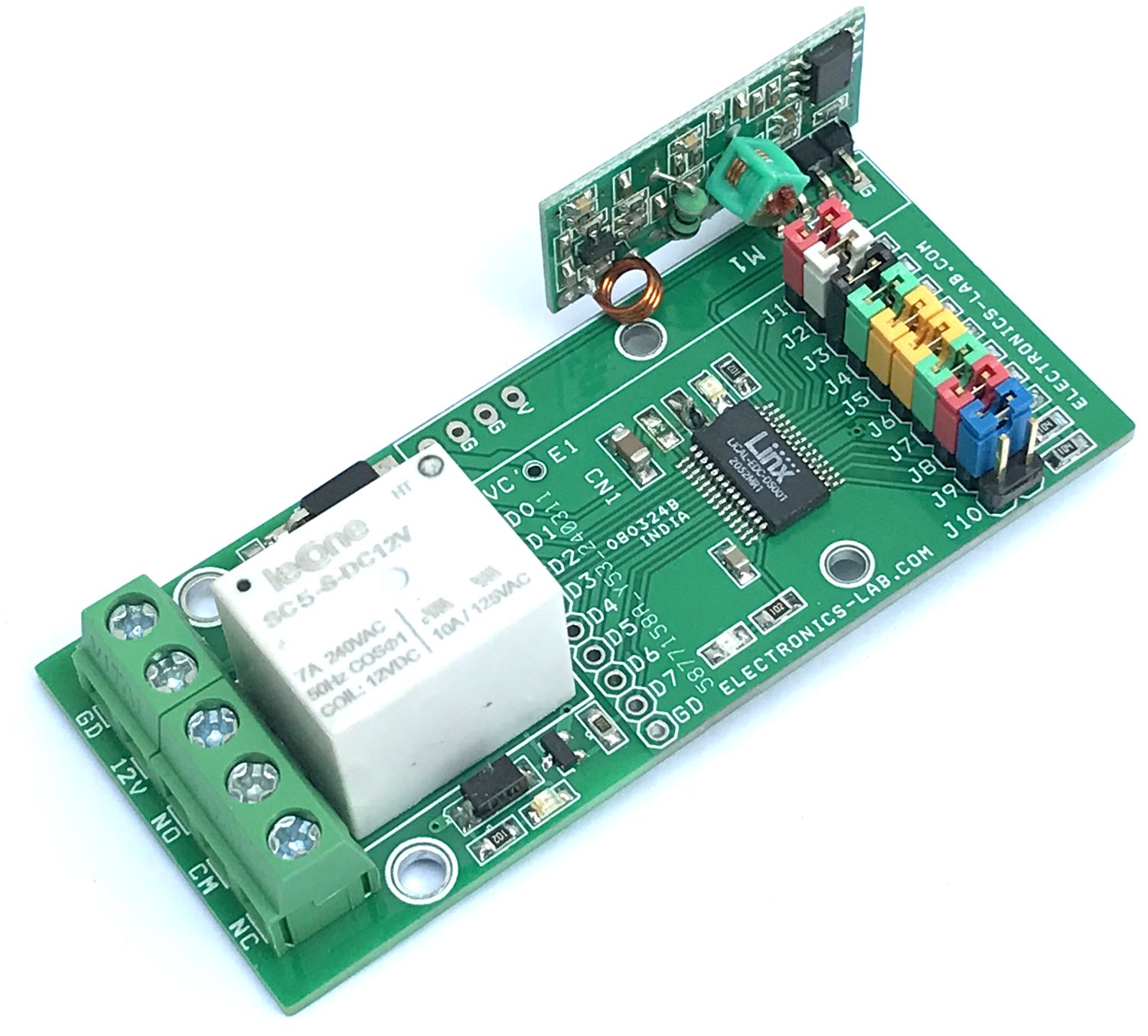
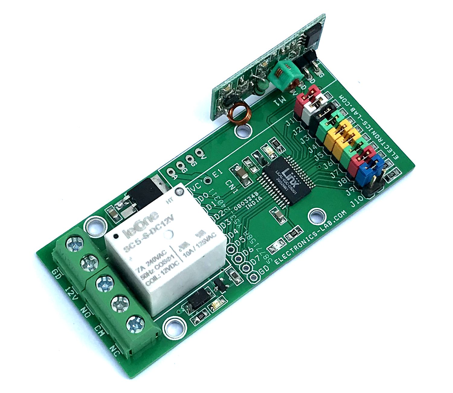
The project described here is one Channel RF remote receiver Relay board. The project is built using LICAL-EDC-DS001 chip from LINX. The board consists of Encoder/Decoder chip, 433Mhz RF Receiver module, 10 x jumpers to set the address, a Relay to drive the output, U2 5V regulator, header connector for data outputs for controlling external devices. All outputs are compatible with TTL logic, normally they are low and go high when a valid signal is received and decoded by the chip. D2 onboard Power LED, D1 LED indicates valid transmission signal. LED D4 shows the relay operations. The relay is connected to the D7 output. The rest D0 to D6 outputs are free and can be used to interface with another device using connector CN1. The relay board will act with D7-Switch 8 of the Remote Transmitter. The relay delivers momentary switching to a load up to 7A DC or AC. It can drive inductive, resistive, and capacitive loads such as Lamps, fans, solenoids, DC motors, AC motors etc.
10 Address Lines Selected through Jumpers J1 to J10
Relay Connected to D7 Data Output
On Board 5V Regulator
7 Data Output TTL Compatible Normally Low (Momentary)
On Board Power LED
On Board VT LED (Valid Transmission)
ON Board Relay LED
Relay Contacts Normally Open/Normally Closed
Relay Contacts 7A/250V AC
PCB Dimensions 45.09 x 33.02 mm
2 x 2.5 mm Mounting Holes
4 x 3 mm Mounting Holes
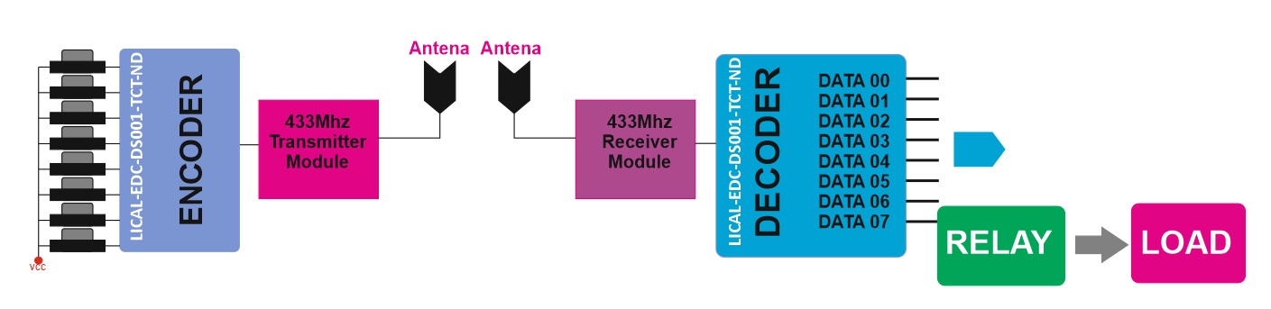
System Configuration
A simple remote-control system consists of an encoder, RF transmitter, RF receiver and a decoder. The encoder is connected to 8 buttons, The encoder detects the closure of one of the switches and converts that into a digital data stream. This data is then sent to an RF transmitter that conveys this data into free space. An RF receiver receives the data and sends it to a decoder. The decoder analyses the data and, if it is valid, replicates the switch closure on an output. This output is then connected to whatever circuitry is to be controlled. All outputs are momentary and TTL logic.
This DS series decoder and encoder chip is ideal for remote control applications. It decodes the signal received by 433 MHz RF modules. When the DS enters Decoder Mode, it checks the state of the DIN line. If it is high, the P_SEL line is checked to set which protocol is used and the decoder receives the data. It compares the address in the received packet to its local address lines. If they match, the data is stored and a second packet is received. With the Holtek® protocol, the decoder compares the two packets. If they match, the received data bits are output on the data lines and the VT line is pulled high thus LED D1 is on. This protocol compares each packet with the previous one looking for a match. The serial protocol requires two matching packets for initial activation and then updates the lines on each subsequent packet. The DS then looks for the next packet on the DIN line. With the Holtek® protocol, once no valid data is received (there is a mismatch of address, data, or bit timings), the Data and VT lines are pulled low and the DS goes to sleep until DIN is pulled high. The Serial protocol holds the output states until a 130ms timer runs out. The Holtek® protocol compares two packets and, if they match, sets the outputs. If a data line is toggled during a transmission (D1 is activated while D0 is already active) then the received packet does not match the previous packet and the output lines are pulled low until the next packet arrives. This causes all of the outputs to briefly cut out when a line is toggled. The serial protocol uses a timer to prevent this cutout.
LICAL-EDC-DS001 Encoder/Decoder Chip
The same part can be used as encoder or decoder by selecting state of one pin. The DS Series also has two protocols built into the same part, selected by the state of a single pin. One is compatible with Holtek devices, such as the HT640 and HT658. The other protocol is a serial data structure that is much more immune to noise and edge jitter. This protocol offers much more range and reliability than the Holtek protocol while keeping the simple jumper-addressing.
Theory of Operation
The DS Series is a remote-control encoder and decoder that offers two protocols in one part based on the state of the P_SEL line. The first protocol operates with the Holtek® HT640 encoder and HT658 decoder. The second is a serial protocol that offers more noise immunity and faster response time while keeping the simple addressing. The DS can operate as either an encoder or decoder based on the state of the E/D_SEL line. It does not operate as both simultaneously. When set as an encoder it monitors the state of the TE line. When the line is high the DS records the states of the data and address lines, assembles them into a packet and outputs the packet three times. The data lines can be connected to switches or contacts. The address lines can be set with Jumpers. When set as a decoder the DS receives packets and validates them. The validation includes checking the bit timings and comparing the received address to the local address line settings. Two matching packets must be received consecutively. If the timings are good and the addresses match, the DS sets its data lines to match the received states. These lines can be connected to the application circuitry to be controlled. When the TE/DIN line is low, the DS goes into a low power sleep mode.
Setting the Address
The project has ten address lines. This allows the formation of up to 1,022 (210 – 2) unique transmitter-receiver relationships, Jumper J1 to J10 can be used to set the address, all lines are pulled high. The chip rejects packets with addresses set to all high or all low. At least one address line must be different from the rest. The encoder does transmit all addresses, but the decoder rejects packets with all address lines set the same. The receiver’s address line states must match the transmitter’s exactly for a transmission to be recognized. If the addresses do not match, then the decoder takes no action.
Initial Operation
On power-up, the E/D_SEL line is tested to determine if the DS operates as an encoder or a decoder. If the line is high, the DS enters Encoder Mode. If low, it enters Decoder Mode. This is checked once on power-up. Once the operating mode is selected, the data-line direction is set. In either mode a rising edge on the TE/DIN line wakes the device from low-power sleep.
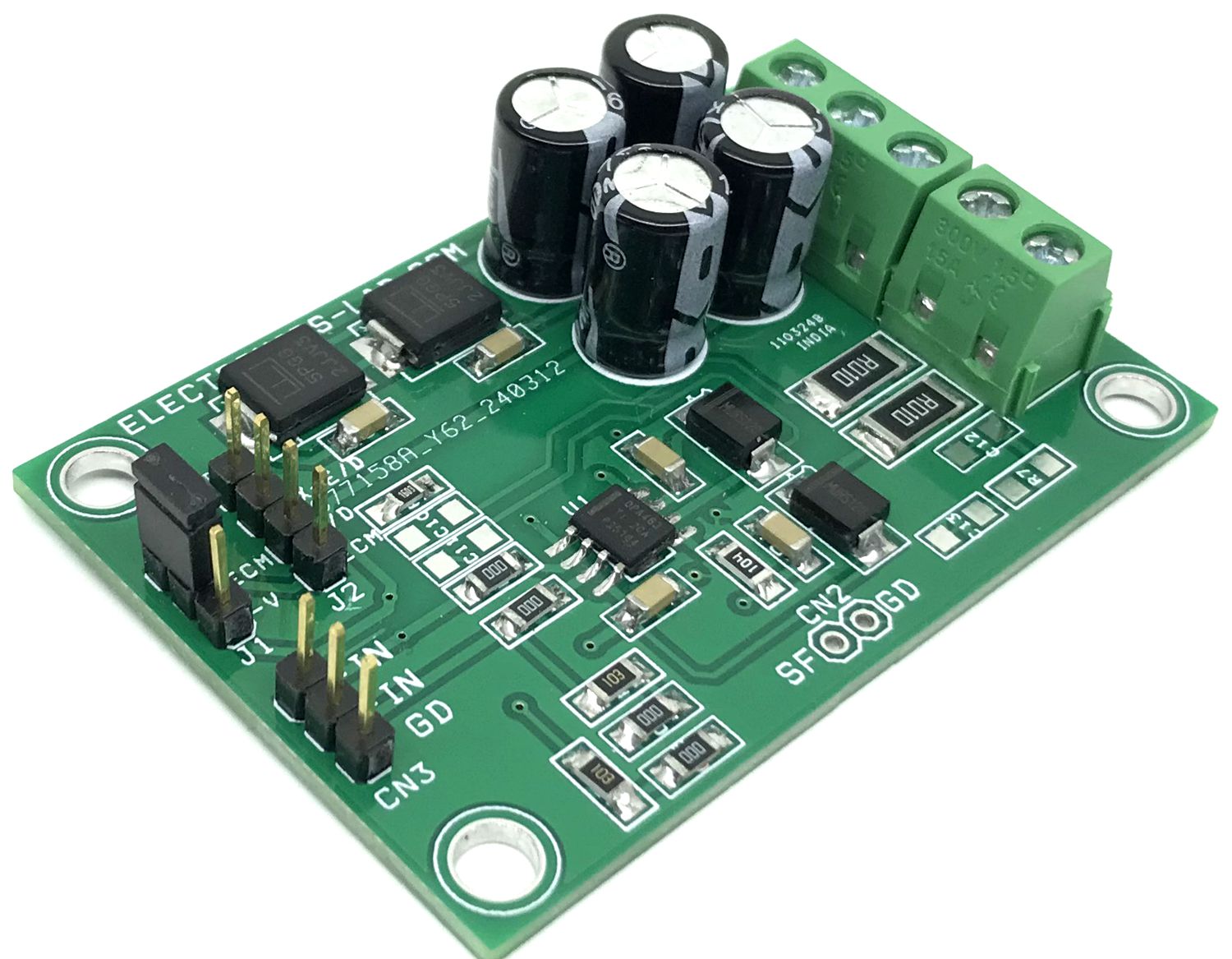
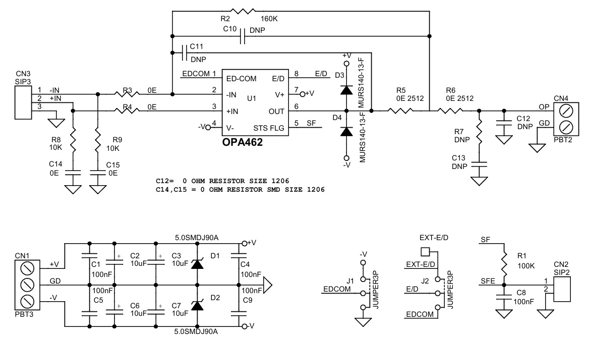
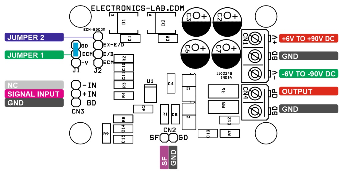
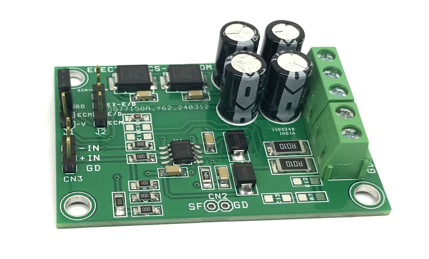
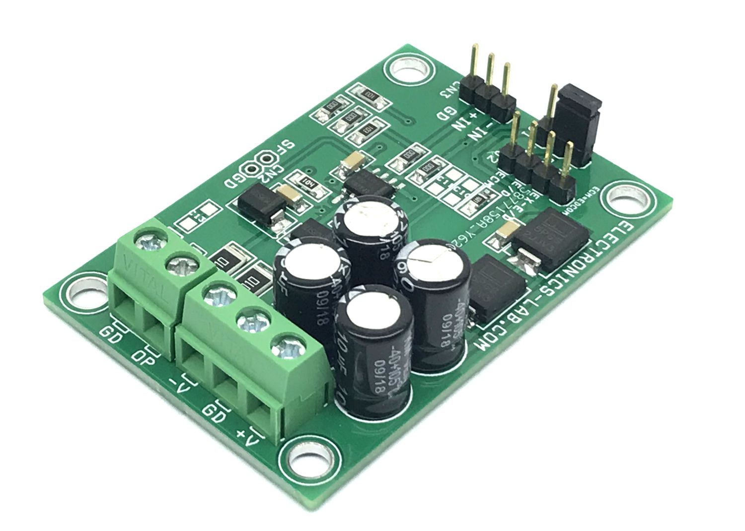
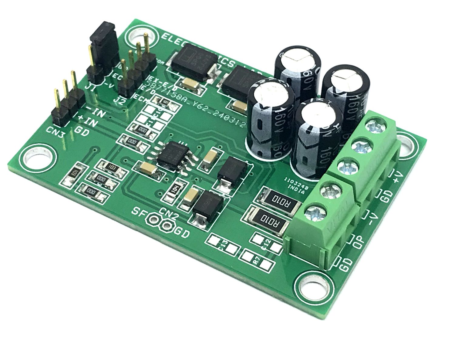
This project provides a platform to evaluate the OPA462 high-voltage, high-current operational amplifier. Multiple component footprints allow the most common circuit configurations. The board accommodates high-voltage and high-current operational amplifier OPA462 from Texas Instruments. A High-Voltage Noninverting Amplifier, AV = 17 V/V. An example application circuit is given below. The board is capable of operating with supply voltages as high as ±90 V (180 V), or as low as ±6 V (12 V). The high-voltage process and design of the OPA462 allow the device to be used in applications where most operational amplifiers cannot be applied, such as high-voltage power-supply conditions, or when there is a need for a very high-output voltage swing. The output is capable of delivering up to ±30 mA output current or swinging within a few volts of the supply rails at moderate current levels. The OPA462 features input overvoltage protection, output current limiting, thermal protection, a status flag, and enable-disable capability. The output swing is 85V with 5V AC signal input and frequency 10Khz. Status Flag is an open-drain active-low output referenced to E/D Com. This pin goes active for either an overcurrent or overtemperature condition. Close (Link) Shunt between GD and E/D Com to enable the output, and Close E/D and E/D Com Jumper J2 to disable the Output.
For Normal operation connect Jumper/Shunt between GD and E/D Com, Jumper J2 open. Use 0 ohms resistors of 1206 Size instead of capacitors C14 and C15. Many optional components are provided for different applications, all capacitors and resistors are SMD 1206. R5 and R6 resistors are SMD 2512 size.
Features
Wide power-supply range:
±90 V (180 V) (Supply Range ±6 V (12 V) to ±90 V (180 V)
High-output load drive: IO ±45 mA
Output Voltage 85V
Input Signal 5V AC
Gain 17V/V
Flexible design allows a wide variety of circuit configurations
Includes protection against power supply sequencing and inductive load kickback
Current limit protection
Thermal protection
Status flag Output
Independent output disables
Gain bandwidth: 6.5 MHz
Slew rate: 32 V/µs
4 x 4 mm PCB Mounting Holes
Screw Terminals for Power Input and Output
Header Connector for Signal Input
Jumper J1 and J2 for Enable/Disable
PCB Dimensions 60.96 x 41.28 mm
A noninverting circuit with a moderately high closed-loop gain (AV) of 17 V/V (24.6 dB). In this example, a 5-VPK ac signal is amplified to 85VPK across a 10-kΩ load resistor connected to the output. The peak current for this application is 8.5 mA, and is well within the OPA462 output current capability. Higher output current, typically up to 30 mA, may be attained at the expense of the output swing to the supply rails. A ±90-VDC power supply is required for this configuration. The noninverting amplifier circuit shows the OPA462 enable-disable function. When placed in disabled mode the op amp becomes non-functional, and the current consumption is reduced to approximately one-third to one-half the enabled level. An enable active state occurs when the E/D pin is left open, or is biased 3 V to 5 V greater than the E/D Com voltage level. If biased between the E/D com level, to E/D Com + 0.65 V, the OPA462 disables. Diode provided at output to protect against back electromagnetic force (EMF).
A potentially destructive mechanism is the back EMF transient that can be generated when driving an inductive load. D3, D4, D1 and D2 in circuit have been added to the basic OPA462 amplifier circuit to provide protection in the event of back EMF. If the voltage at the OPA462 output attempts to momentarily rise above V+, D3 becomes forward-biased and clamps the voltage between the output and V+ pins. This clamp must be sufficient to protect the OPA462 output transistor. If the event causes the V+ voltage to increase the power supply bypass capacitor, D1, or both, a Zener diode or a transient voltage suppressor (TVS) can provide a path for the transient current to ground. D4 and D2 provide the same protection in the negative supply circuit.
The OPA462 noninverting amplifier circuit with a closed-loop gain of 17 V/V has a small-signal, –3-dB bandwidth of nearly 800 kHz. However, the large-signal bandwidth is likely of greater importance in a high-output-voltage application. For that mode of operation, the slew rate of the op amp and the peak output swing voltage must be considered in order to determine the maximum large-signal bandwidth. The slew rate (SR) of the OPA462 is typically 6.5 V/µs, or 6.5 × 10⁶ V/s.
The best practice for a typical parameter such as slew rate to allow for variance. In this example, keeping the large signal fMAX to 10 kHz is sufficient to make sure the output avoids slew rate limiting
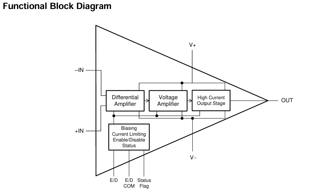
The OPA462 is a high voltage (180V) and high current drive (45 mA) operational amplifier. The device is unity-gain stable and has a gain-bandwidth product of 6.5 MHz The OPA462 is internally protected against over-temperature conditions and current overloads. The device is fully specified to perform over a wide power-supply range of ±6 V to ±90 V, or on a single supply of 12 V to 180 V. The status flag is an open-drain output that allows the device to be easily referenced to standard low-voltage logic circuitry. This high-voltage operational amplifier provides excellent accuracy and wide output swing, and is free from phase inversion problems that are often found in similar amplifiers. The output can be disabled using the enable-disable (E/D) pin. The E/D pin has a common return pin to allow for easy interface to low-voltage logic circuitry. This disable is accomplished without disturbing the input signal path, not only saving power but also protecting the load.
Status Flag Pin
The Status Flag pin indicates fault conditions and can be used in conjunction with the enable-disable function to implement fault control loops. This pin is triggered when the device enters an overtemperature or overcurrent fault condition. This pin is an open-drain, active-low output that allows the pin to be easily interfaced with standard low-voltage logic. The pin goes active if the junction temperature of the device rises to greater than 150°C, and resets after the device cools to 130°C. Additionally, the pin goes active if the device attempts to source more than the maximum continuous current of 30 mA. The status flag can be monitored from Pin 1 of CN2.
Thermal Protection
The OPA462 features internal thermal protection that is triggered when the junction temperature is greater than 150°C. When the protection circuit is triggered, thermal shutdown occurs to allow the junction to return a safe operating temperature. Thermal shutdown enables the Status Flag pin, which indicates the device has entered the thermal shutdown state.
Current Limit
Current limiting is accomplished by internally limiting the drive to the output transistors. The output can supply the limited current continuously, unless the die temperature rises to 150°C, which initiates thermal shutdown. With adequate heat dissipation, and use of the lowest possible supply voltage, the OPA462 can remain in current limit continuously without entering thermal shutdown. The best practice is to provide proper heat dissipation (either by a physical plate or by airflow) to remain well below the thermal shutdown threshold. For longest operational life of the device, keep the junction temperature below 125°C.
Enable and Disable
If left disconnected, E/D Com is pulled near V– (negative supply) by an internal 10-μA current source. When left floating, E/D is held approximately 2 V above E/D Com by an internal 1-µA source. Even though active operation of the OPA462 results when the E/D and E/D Com pins are not connected, a moderately fast, negative-going signal capacitively coupled to the E/D pin can overpower the 1-µA pullup current and cause device shutdown. This behaviour can appear as an oscillation and is encountered first near extreme cold temperatures. If the enable function is not used, a conservative approach is to connect E/D through a 30-pF capacitor to a low impedance source. Another alternative is the connection of an external current source from V+ (positive supply) sufficient to hold the enable level above the shutdown threshold. Figure 60 shows a circuit that connects E/D and E/D Com. The E/D Com pin is limited to (V–) + 100 V to enable the use of digital ground in a application where the OPA462 power supply is ±90 V. When the E/D pin is dropped to a voltage between 0 V and 0.65 V above the E/D Com pin voltage the output of the OPA462 will become disabled. While in this state the impedance of the output increases to approximately 160 kΩ. Because the inputs are still active, an input signal might be passed to the output of the amplifier. The voltage at the amplifier output is reduced because of a drop across this output impedance, and may appear distorted compared to a normal operation output. After the E/D pin voltage is raised to a voltage between 2.5 V and 5 V greater than the E/D Com, the output impedance returns to a normal state and the amplifier operates normally.
Connections
CN1: Pin 1 = +6V to 90V DC Power, Pin 2 = GND, Pin 3 = -6V to -90V
CN2: Pin 1 = SF (Fault Output), Pin 2 GND
CN3: Pin 1 – Input (No Use for Non-Inverting Application), Pin 2 +Input Signal, Pin 3 = GND
CN4: Pin 1 Output, Pin 2 GND
J1: Jumper J1 and J2 Enable/Disable, enable = Connect EDCOM and GND, J2 Open
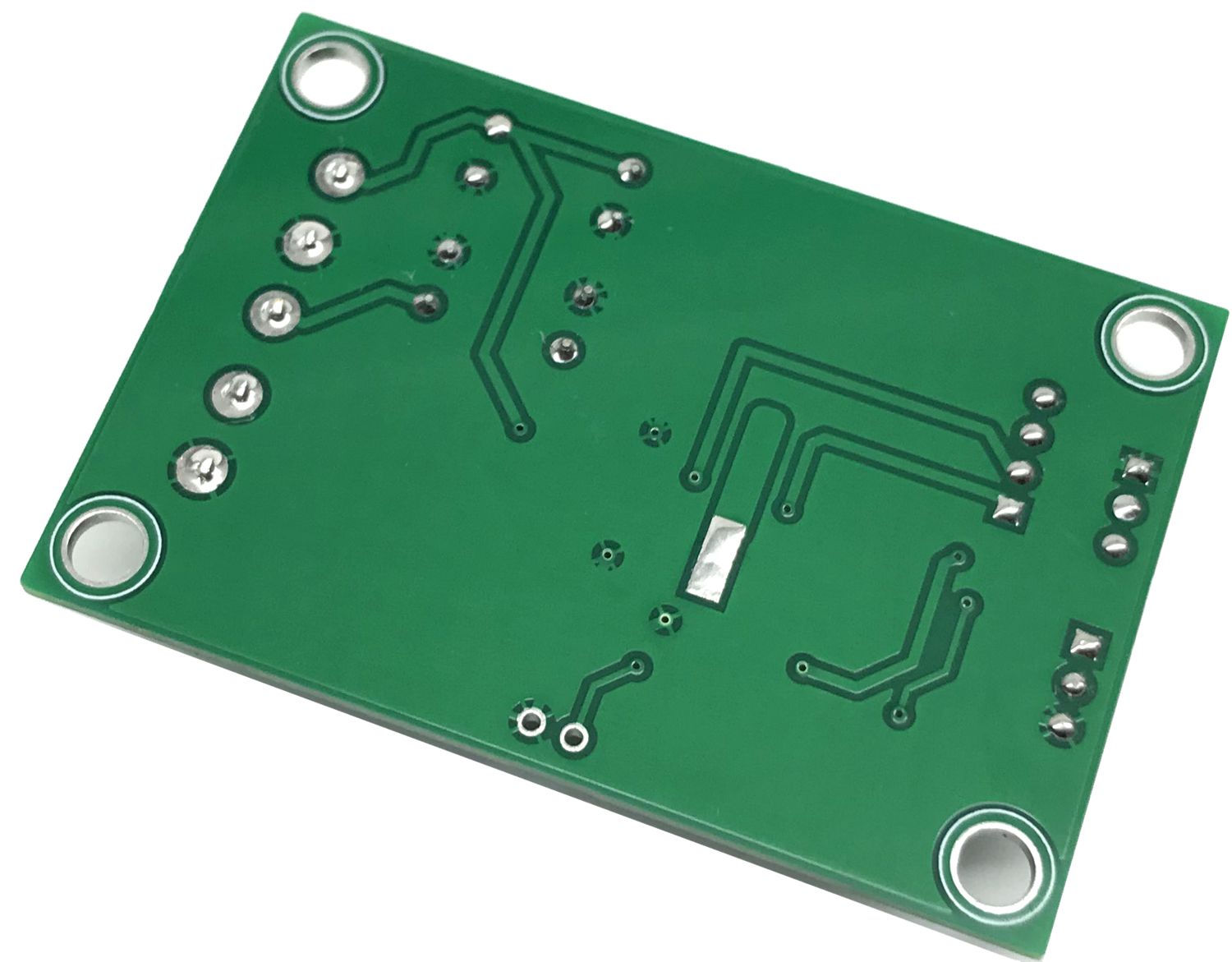
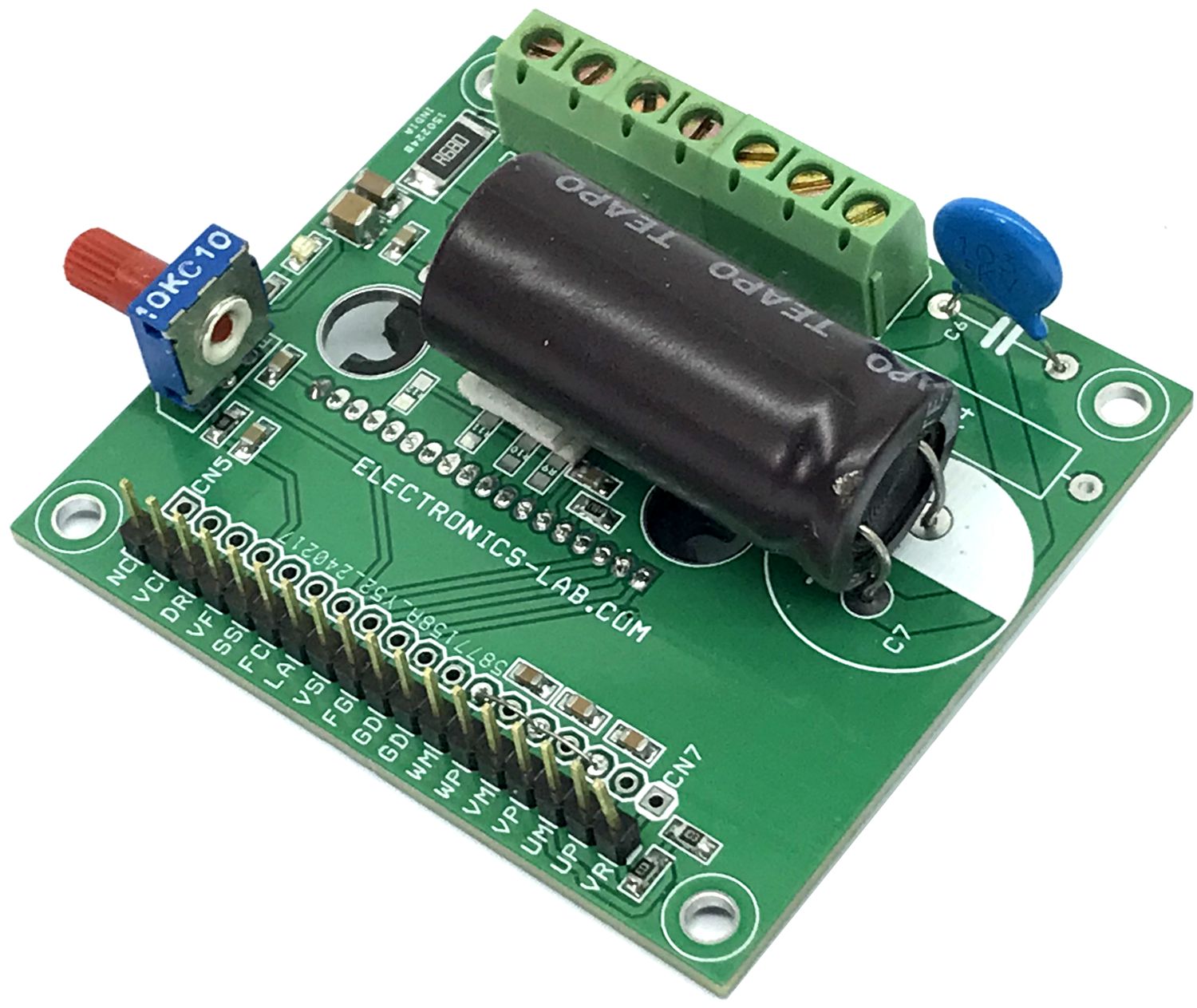
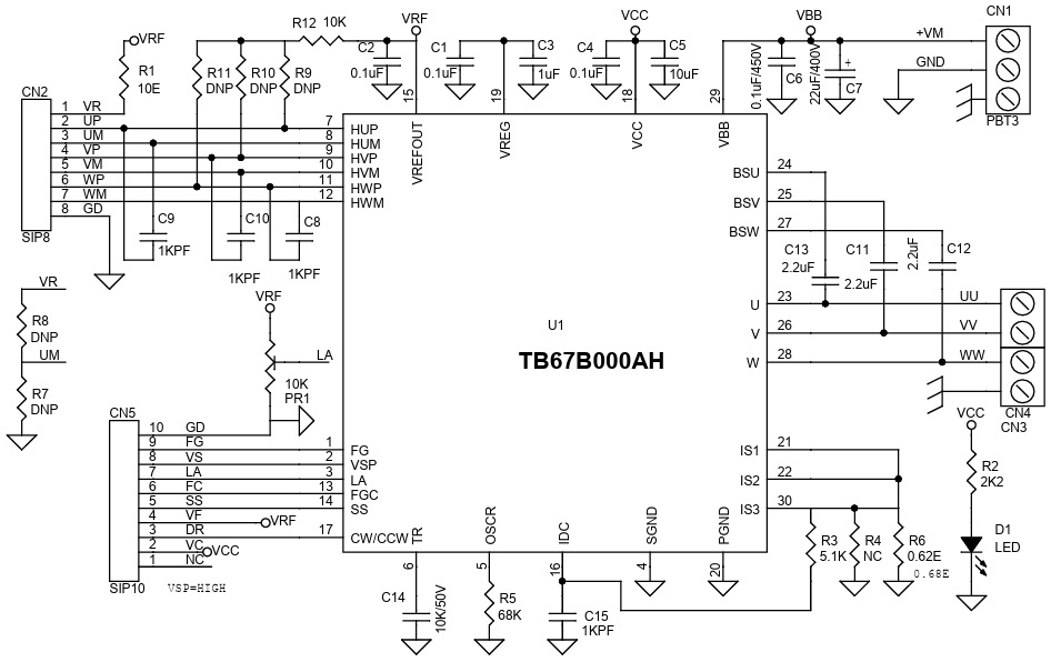
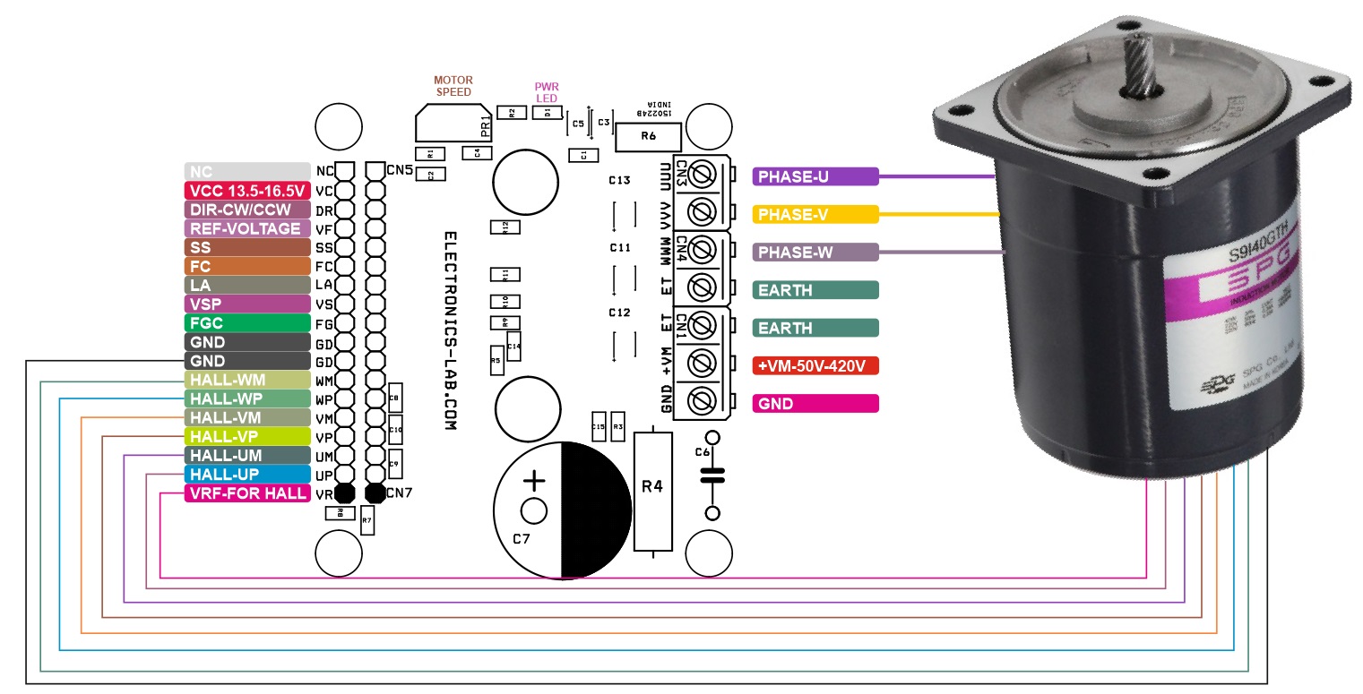
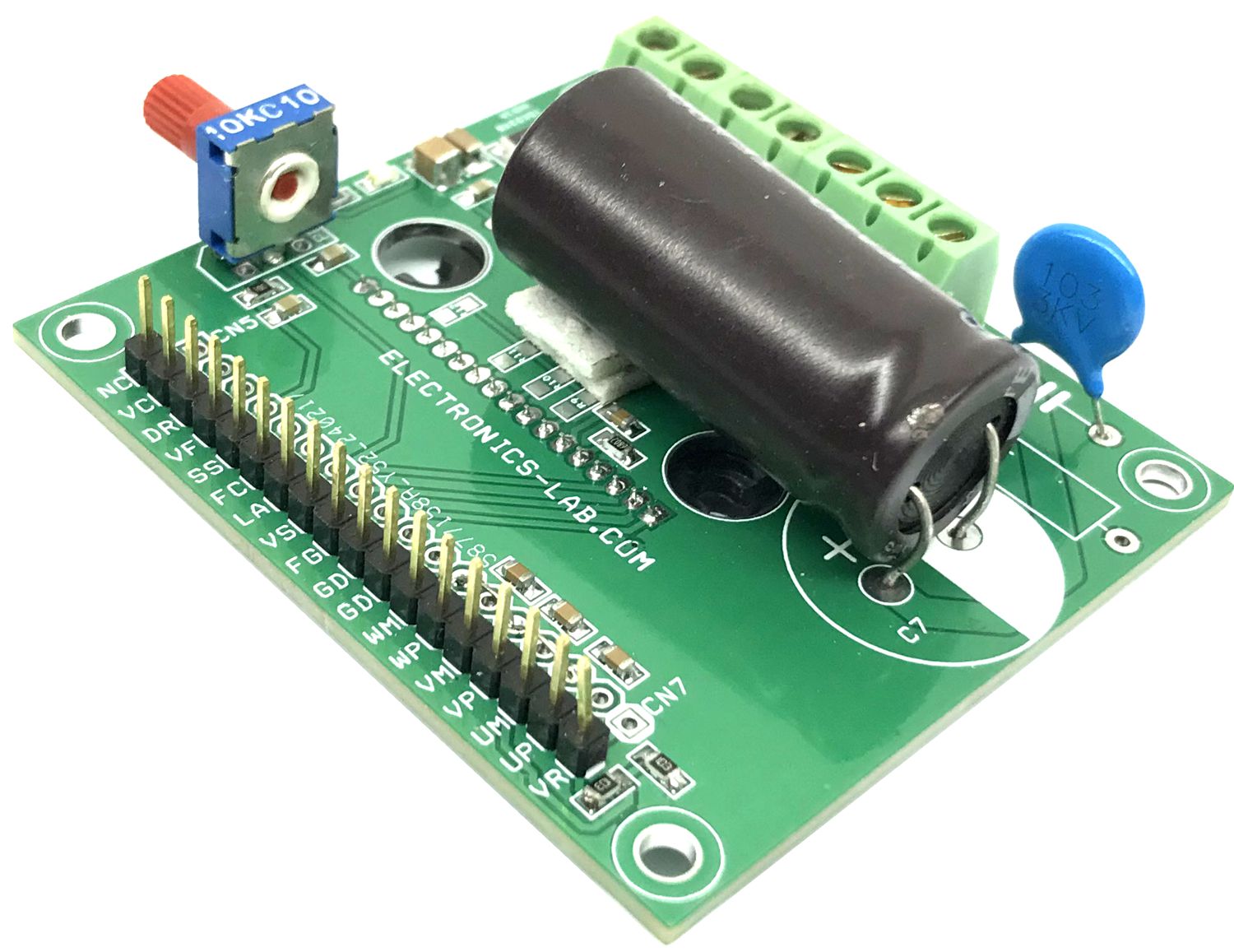
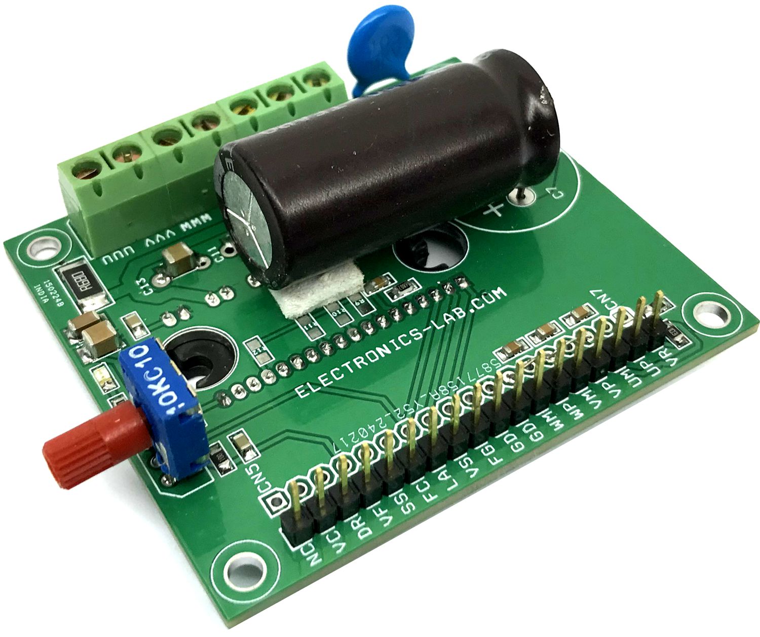
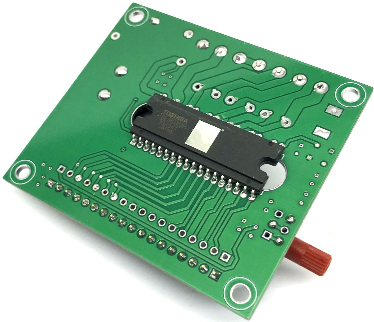
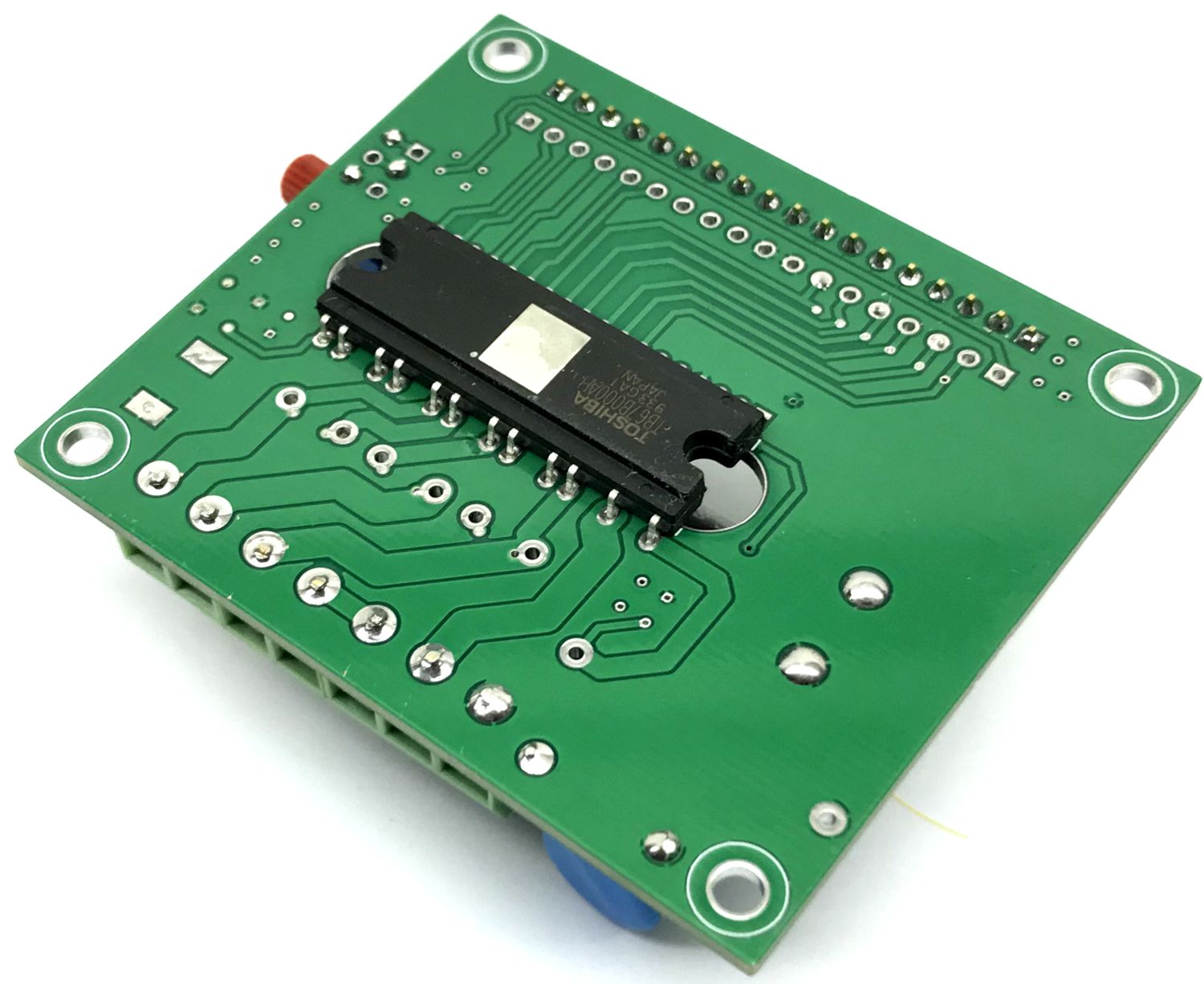
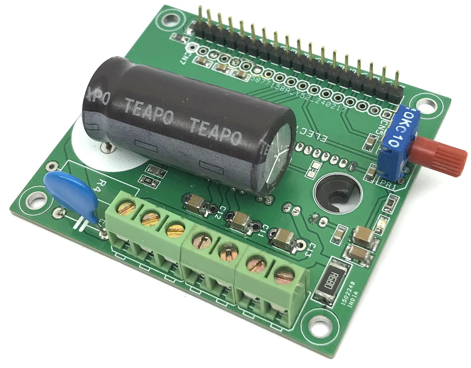
The project presented here is a three-phase sinewave PWM driver for high-voltage brushless motors. The board is built using TB67B000AHG chip, which is a high-voltage IC capable of handling 600V. The TB67B000AHG has a 2-in-1 (MCP) structure of controller (sine-wave PWM / wide-angle conduction) and a high-voltage driver. The rotation speed of a DC brushless motor can be controlled directly by the speed control signal (analog voltage) by an onboard trimmer potentiometer or from a microcontroller. The board supports a 3-phase BLDC motor with Hall sensors. On Board Trimmer, the potentiometer helps users to control the speed of the brushless motor.
The TB67B000AHG is a high-voltage PWM brushless motor driver. The IC integrates a controller, which supports sinewave PWM drive with wide-angle commutation, and a high-voltage driver in a single package (“two-in-one”, i.e., MCP). It is designed to change the speed of a brushless motor directly.
Note 1: It is important to install a heatsink before conducting any test.
Note 2: The Driver supports a dual output hall sensor, for a single output hall sensor, Install R7 and R8 = 20K Ohms SMD size 0805, Tie UM, VM, WM pins of CN2. Use UP, VP, and WP Pins for 3 Hall sensors.
Note 3: The board operates at lethal voltages and has bulk capacitors that store significant charge. Accidental contact can lead to lab equipment damage, personnel injury, and may be fatal. Please be exceptionally careful when probing and handling this board. Always observe normal laboratory precautions.
Note 4: Since the board operates at lethal voltages, use a plastic shaft for the trimmer potentiometer. Avoid metal shaft potentiometer.
Features
Operating power supply voltage range: VCC = 13.5 to 16.5 V
Motor power supply operating voltage range: VBB = 50 to 420 V (Up to 450V, Limited due to Capacitor Voltage)
A Controller and a high-voltage driver integrated in a single package.
Sine-wave PWM drive or wide-angle commutation drive is selectable.
Built-in oscillator circuit (carrier frequency = fosc/252 (Hz))
Bootstrap circuitry: Built-in bootstrap diode
Built-in overcurrent protection, thermal shutdown, undervoltage lockout, and motor-lock detection.
Internal voltage regulator circuit (VREG = 5 V (typ.), 30 mA (max), Vrefout = 5 V (typ.), 35 mA (max))
PCB Dimensions 64.77 x 57.15 mm
4 x 3.2 mm Mounting Holes
2 x 8 mm Holes for Heat-Sink
Sequence of power supply
Sequence of power supply: Please supply the power by following the procedure of (1) to (3).
Apply power supply of VCC. (Power Supply for Controller Chip)
In applying Vcc, connect Vsp to GND or open. (VSP=VS On PCB)
In case terminals of CW/CCW, LA, and SS are controlled by signals of external IC, connect them to GND or open. After applying power supply of VCC, set the terminal of CW/CCW, LA, and SS high-level if needed.
Apply power supply of VBB. (Motor Power)
Apply voltage to Vsp.
Sequence of power shutdown: Please shut down the power by following procedures of (1) to (3).
Set Vsp to 0V. ( VSP=VS on PCB)
In case terminals of CW/CCW, LA, and SS are controlled by signals of external IC
After setting Vsp 0V, connect them to GND or open. (VSP=VS On PCB)
Shut down VBB.
Shut down VCC.
Output current
The absolute maximum rating is 2 A which must not be exceeded, even for a moment. Design an actual application system with the IC so as not to make the inrush current and the lockout current exceed the absolute maximum ratings, especially when a motor starts up and gets stuck in the lockout. The available output current depends on the usage conditions(ambient temperature, mounting board method, and so on). Design an actual application system with a sufficient margin in order that Tj does not exceed 150°C.
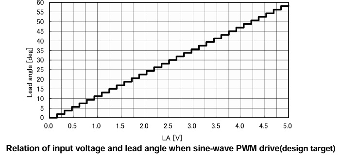
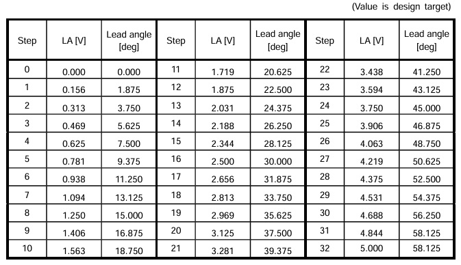
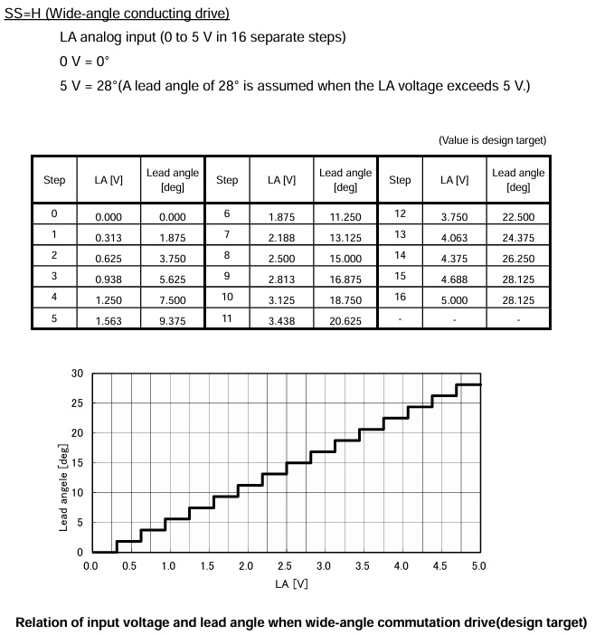
Lead angle control
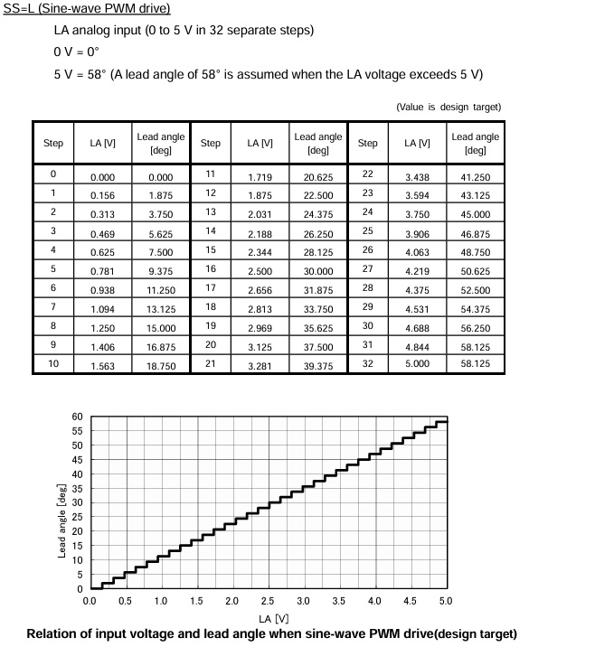
The lead angle of the driver output according to the induced voltage can be adjusted by the input voltage of LA terminal. The range of lead angle is as follows; Sine-wave PWM drive: 0° to 58°, Wide-angle conducting drive: 0°to 28° The efficiency of the motor operation can be improved by adjusting the lead angle. In adjusting the motor characteristics by applying the lead angle, change the lead angle by LA terminal and compare the motor current. Adjust the voltage of the LA terminal in order to minimize the motor current as comparing the motor current before and after changing the lead angle under the condition that the rotation speed is the same.
SS=L (Sine-wave PWM drive)
LA analog input (0 to 5 V in 32 separate steps) 0 V = 0° 5 V = 58° (A lead angle of 58° is assumed when the LA voltage exceeds 5 V)
Oscillator Frequency (Default 20Khz = R5 68K Ohms, If R5 is 75K Ohms Frequency 18Khz)
Oscillation frequency (Fosc) range should be 3.5MHz to 6.4MHz. The relation of the oscillation frequency (Fosc) and the PWM frequency (FC) is as follows; FC=Fosc/252. When R1= 68kΩ, FC=20 kHz (typ.), and when R1= 75kΩ, FC=18 kHz (typ.).
TR terminal
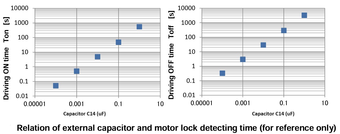
When the motor is locked, the motor lock detection operates and the drive output is turned on and off (intermittent operation). Driving OFF period (Toff) and driving ON period (Ton) can be configured by the external capacitor (C1) of TR terminal. When this function is not used, please connect this terminal to SGND. The relation of external capacitor (C14) and driving ON/OFF period is roughly calculated as follows. ・
Setting time
Driving ON period Ton[s]=C1×(VH―VL) ×2/I×500 counters
Driving OFF period Toff[s]=C1×(VH―VL) ×2/I×3000 counters
When C14 = 0.01μF, I = 3μA (typ.), VH= 2 V (typ.) and VL= 0.5V (typ.), and so
Ton[s]=5s (typ.) and Toff[s]=30s (typ.)
Current Sense Resistor
The relation between the output current (IOUT) and the detecting resistor (R6) is provided roughly in the following formula. IOUT = Vdc/ R6 Voltage of current detection Vdc: 0.475V (min.), 0.5 V (typ.), and 0.525V (max.) Example) When the resistor (R6) is configured 0.51 Ω, IOUT (typ.) = 0.5 V (typ.)/0.51 Ω ∼ − 0.98 A Please determine the rating of the external parts with sufficient margins because large current flows in the detecting resistor (R6). In operating the motor, the power on the detecting resistor (P) is calculated as follows; P=0.525Vx0.525V/ R6 (max.). For example, when R6=0.51Ω, P=0.540W. So, please apply the resistor of 1 W or more as a rated power.
VSP Pin ( On PCB VSP=VS)
Operation and stop of the motor and rotating speed can be controlled by inputting command signal of the output ON duty to Vsp terminal. Please input analog voltage as a command signal. Moreover, when rotation speed needs to be controlled, connect it to MCU with Vsp signal and FG signal and feedback the speed to control the motor rotation number.
FG Pin
Push-pull circuit of 5V output is constructed. When rotation speed needs to be controlled, input FG signal to MCU to use this signal as the information of the motor rotating number.
CW/CCW Pin
In using this terminal by fixing the voltage of the terminal, connect it to Vrefout or SGND. In connecting to Vrefout, it becomes high level. In connecting to SGND, it becomes low level. In using this terminal by inputting the external control signal, input this signal after applying the power supply of Vcc. In shut down, turn off Vcc after the control signal is turned off. In switching the logic of CW/CCW terminal, change the input signal after setting the Vsp terminal 0.7V or less and turning off the operation output. After switching the input signal, start the motor operation by Vsp terminal.
FGC Pin
In using this terminal by fixing the voltage of the terminal, connect it to Vrefout, SGND or Vrefout/2. In connecting to Vrefout, it becomes high level. In connecting to Vrefout /2, it becomes M level. And in connecting to SGND, it becomes low level. In using this terminal by inputting the external control signal, input this signal after applying the power supply of Vcc. In shut down, turn off Vcc after the control signal is turned off.
SS Pin
In using this terminal by fixing the voltage of the terminal, connect it to Vrefout or SGND. In connecting to Vrefout, it becomes high level. In connecting to SGND, it becomes low level. In using this terminal by inputting the external control signal, input this signal after applying the power supply of Vcc. In shut down, turn off Vcc after the control signal is turned off.
HUP, HUM, HVP, HVM, HWP, HWM Pins
Input hall signals to HUP, HUM, HVP, HVM, HWP, and HWM terminals. Select hall elements or hall ICs to provide hall signals. Connect output terminals of U, V, and W, and the hall signal terminals of HUP, HUM, HVP, HVM, HWP, and HWM, to the motor to have the relation shown in the timing chart of “ refer timing chart). Notes in using the motor”. ・If 5V is supplied from the Vrefout power supply to the hall elements, add the limiting resistor to the power supply terminal of the hall element in order to be within the maximum input current of the hall element. ・To recognize switching of the hall signal correctly, the amplitude of the hall elements should be 40 mV or more and the input voltage range should be 0.5 V to 4.0 V. ・Hall amplifier has a hysteresis. When the amplitude of it is small, the phase gap of the switching timing becomes large. So, please make the amplitude of it as large as possible. ・When the capacitor for reducing the noise of the hall signal is attached, please arrange it close to HUP and HUM terminals, HVP and HVM terminals, and HWP and HWM terminals. The recommended capacitor is 0.001 μF to 0.1 μF.
< Notes in using the hall IC> Please configure HUP, HVP, HWP, HUM, HVM, and HWM as follows. It is recommended to adopt low-pass filter between the input terminal and SGND to reduce the noise. However, in this case, delay time of the input signal should be considered.
HUP, HVP, and HWP: Input voltage: H level = Vrefout, L level = SGND HUM, HVM, and HWM: Input voltage: Vrefout/2 * Configure it with resistive dividing voltage between Vrefout terminal and SGND.
HUP, HVP, and HWP: Input voltage: Vrefout/2 * Configure it with resistive dividing voltage between Vrefout terminal and SGND. HUM, HVM, and HWM: Input voltage: H level = Vrefout, L level = SGND
Connections
CN1: Pin1 = +VM Motor Supply 50V to 420V DC, Pin 2 = GND, Pin 3 = GND
CN2: Pin 1 Reference 5V for Hall Sensor, Pin 3=Hall Sensor HUP, Pin 4 = Hall Sensor HUM, Pin 5 = Hall Sensor HVP, Pin 6 = Hall Sensor HVM, Pin 6 = Hall Sensor HWP, Pin 7 = Hall Sensor HWM, Pin 8 = GND
CN3: Pin 1 = Motor W Phase, Pin 2 = Earth
CN4: Pin 1 = Motor U Phase, Pin 2 = Motor V Phase
CN5: Pin 1 = NC, Pin 2 = VCC 13.5V to 16.5V, Pin 3 = Dir CW/CCW (High or Low), Pin 4 = VREF 5V DC, Pin 5 = SS, Pin 6 = FGC, Pin 7 = LA Speed Control Voltage Input, Pin 8 = VSP, Pin 9 = FG, Pin 10 = GND
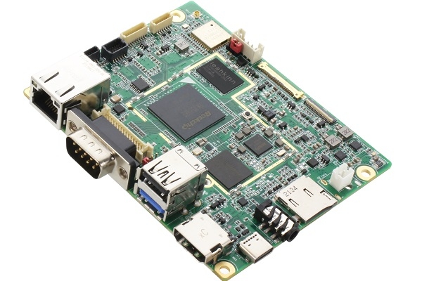
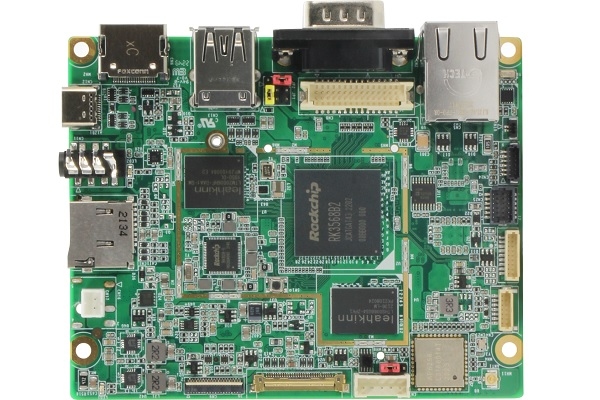
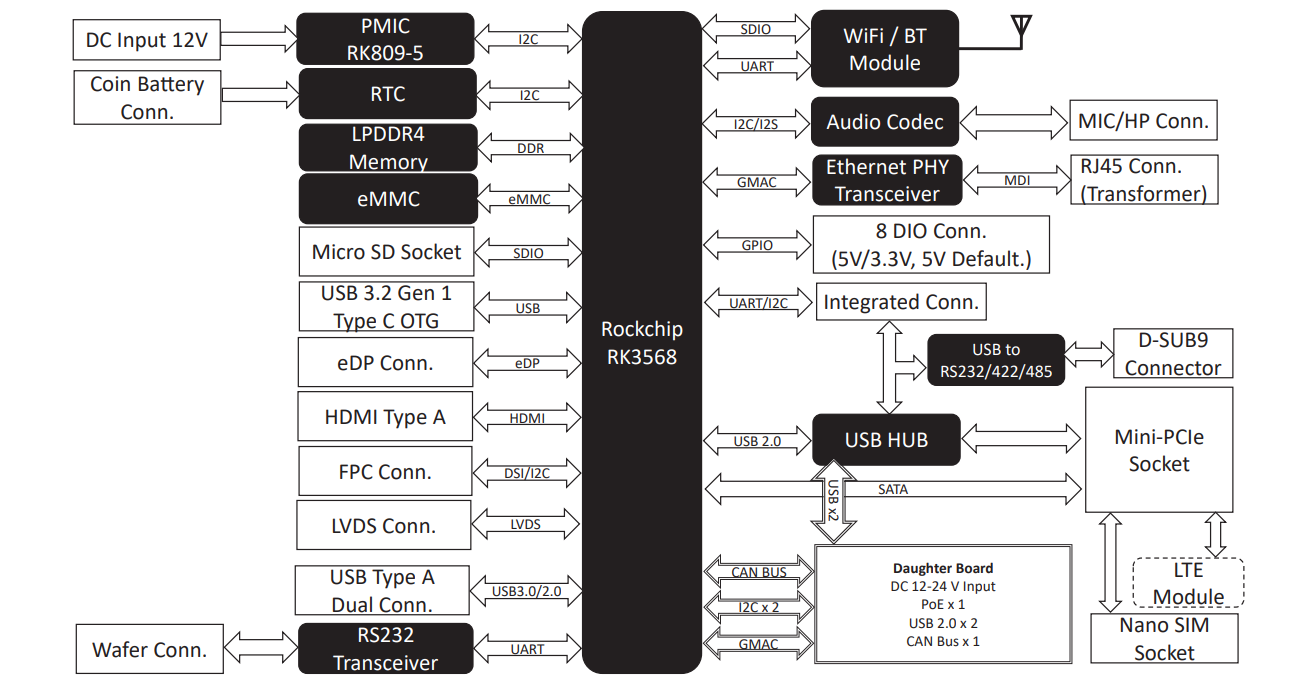
AAEON is now inclining to a slightly wider form factor with its new RICO-3568 based on Rockchip RK3568 Quad-Core Arm® Cortex®-A55 Processor. Adhering to the Pico-ITX Plus form factor which is 100mm x 80mm in dimension, it seems the extra 8mm in its size compared to the array of AAEON Pico-ITX Boards, this one has more scope for interfaces.
The Rockchip RK3568 in the RICO-3568 means an integrated NPU with 0.8 TOPS and an Arm® Mali™-G52 GPU accompanying this Pico-ITX Fanless Board. The memory interface of RK3568 supports 32-bit DDR4, DDR3L, LP4, and LP4x with ECC, but the RICO-3568 optionally has Onboard LPDDR4 up to 8GB, while for storage the board is equipped with 16GB eMMC and Micro-SD card, along with a full-size mini-PCIe slot.
Interfaces of RICO-3568:
The RICO-3568 is equipped with several interfaces:
Wi-Fi 802.11 a/b/g/n/ac, BT V5.0
Display interfaces:
HDMI 2.0, up to 4K x 2K @ 60Hz (video decode)
eDP 1.3, up to 2560 x 1600 @ 60Hz (video encode)
18/24-bit LVDS, up to 1280 x 800 @ 60Hz; JP2, 3.3V/5V: LVDS Power Selection;n
LCD Backlight connector; JP3, 5V/12V: Backlight Power Selection
MIPI DSI up to 2048 x 1536 @ 60Hz for dual-MIPI mode
Audio: Microphone/ Earphone (3.5mm)
Networking ports:
1x Gigabit Ethenret RJ45 port
Optional Gigabit Ethernet RJ45 port via T650 daughter board or T650 Wide-Voltage board for dual GbE and PoE support
WiFi 5 802.11 a/b/g/n/ac and Bluetooth 5.0 + EDR with u.FL antenna connector
Optional WiFi 6 or 4G LTE via mini PCIe socket and NanoSIM push-push type slot
USB
1x USB 3.2 Gen 1 OTG Type-C port
1x USB 3.2 Gen 1 port
1x USB 2.0 Type-A port
1x USB 2.0 interface via pin Header with integrated USB, I2C, 5V
Serial
RS-232/422/485 DB9 connector; JP1, 5V/12V: RS-232/422/485 Voltage Output Selection
7-pin RS-232 Debug wafer
CN3: UART (Tx/Rx only), I2C, USB, Others
The RICO-3568 allows a few expansions. It includes a full-size mini-PCIe slot, which supports both mSATA and USB devices, providing flexibility for storage and peripheral connectivity. Additionally, eight GPIO pins are accessible via a 2×6-pin Wafer, allowing for various custom hardware integrations. A 40-pin FPC connector further expands its functionality, supporting a daughter board that includes CAN Bus for automotive applications, two I2C interfaces for connecting sensors and other I2C devices, and GMAC for Ethernet connectivity, enhancing its suitability for diverse smart building and industrial applications.
What makes RICO-3568 robust
AAEON claims the RICO-3568, with its wide array of interfaces, is a robust, RISC-V based fanless industrial-grade solution for applications such as automation, digital signage, and edge computing. This could be owed to its versatile power supply options, including +12V DC input and optional Power over Ethernet (PoE). Its compact size (100 x 80mm) and lightweight design (200 grams) make it suitable for space-constrained environments. The board operates reliably within a wide temperature range (0°C to 60°C, with an optional -20°C to 60°C) and high humidity tolerance (0% to 90% relative humidity).
AAEON also provides Android 12 and Debian 10 support for the board, whilst, available documentation includes a datasheet and user manual mostly focusing on the hardware. More information on the RICO-3568 Pico-ITX Fanless Board with Rockchip RK3568 Quad-Core Arm® Cortex®-A55 Processor is available on the product page.
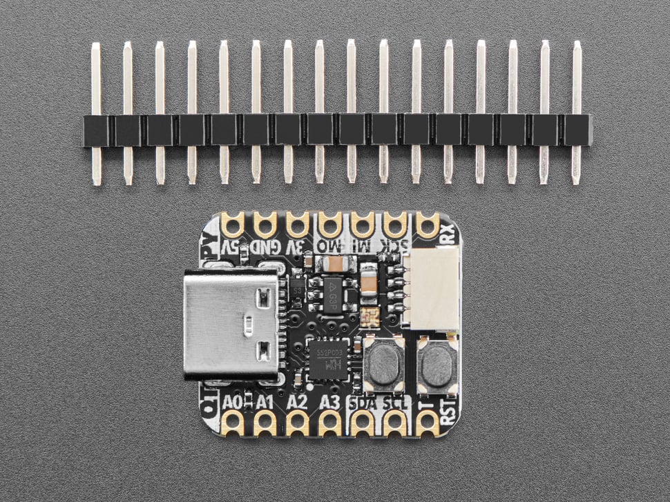
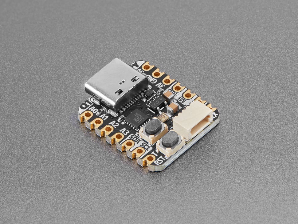
Adafruit just announced Adafruit CH552 QT Py and this board ranks in the top part of my weird tech list. The MCU used in this is a WinChipHead (WCH) CH552 has an E8051 Core. with 16 kilobytes of flash memory but only about 1.25 kilobytes of RAM, and the most weird thing about this it has a built-in USB physical interface (PHY).
An 8051 with USB! surprising but true. The QT Py follows the tiny Seeed Studio Xiao form factor, measuring just 20 by 17.5 millimeters. It features a microcontroller with a USB-C interface for programming and an RGB NeoPixel LED for visual feedback. With 10 GPIO pins and castellated edges, it offers flexibility for soldering header pins or direct attachment to a circuit board.
The CH552 has specific programming requirements and doesn’t support MicroPython or CircuitPython. If using the Arduino IDE, you’ll need the ch55xduino board support package, which has a limited-feature compiler. Not all Arduino libraries are compatible, so testing example code is advisable. Check out Toby Chui’s project for an example using the CH552: a hotplate controlled by the CH552 to regulate the heating profile.
Adafruit CH552 Specifications:
Compact, Seeed Xiao-compatible design
USB Type-C connector with Micro B adapter compatibility
A2 pin serves as MOSI for hardware SPI and one of only 4 ADC pins
4 x 8-bit analog inputs (A0-A3)
3 x PWM outputs
I2C port with STEMMA QT plug-n-play connector
Hardware UART and SPI
4 x Capacitive Touch inputs on A0-A3 pins, no extra components needed
3.3V regulator with 600mA peak output
Reset switch and bootloader for easy code restart or USB ROM bootloader mode entry
Adafruit is now offering the CH552 8051 QT Py at an enticing price of $4.95. This adorable board is readily available, inviting you to delve into its distinctive features and capabilities.
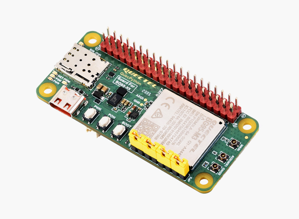
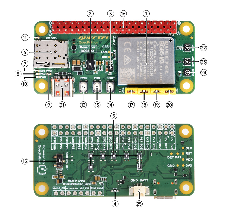
Waveshare recently listed Quectel BG95-M3 Zero, a BG95-M3 powred dev board Raspberry Pi Zero form factor. The dev board is designed for IoT applications and features LTE Cat M1 (eMTC), LTE Cat NB2 (NB-IoT), and eGPRS along with GNSS. As the form factor is compatible with Pi Zero, it supports Raspberry Pi HATs and ships preloaded with QuecPython MicroPython firmware.
While the official documentation primarily focuses on the Windows-based QPYcom program, the Quectel BG95-M3 module can be programmed with MicroPython using plugins for Thonny IDE or Microsoft VSCode, eliminating the need for a Windows machine. The Thonny IDE plugin, specifically, can be found on the official QuecPython GitHub repository, offering an alternative development environment for users on other operating systems.
The QPYcom program, available exclusively for Windows, serves as the primary development environment for the Quectel BG95-M3 module. QPYcom offers a range of features for debugging code, analyzing logs, transferring files, flashing firmware, and even “merging” firmware. However, the Windows-only limitation might be inconvenient for some users. Additionally, the company recommends disabling antivirus software before installation, raising potential security concerns. Detailed instructions and further information can be found in the official Wiki.
GNSS Positioning: Supports GPS, GLONASS, BDS, Galileo, and QZSS.
Nano SIM Card Slot: Supports 1.8V SIM card, designed for easy insertion/removal.
MIPI Interface: Supports MIPI screen and Raspberry Pi peripherals.
Camera Interface: Supports customized SPI camera up to 30MP.
Development Tools: QPYcom, Thonny IDE plugin, VSCode plugin.
Power Supply: 5V via USB-C port
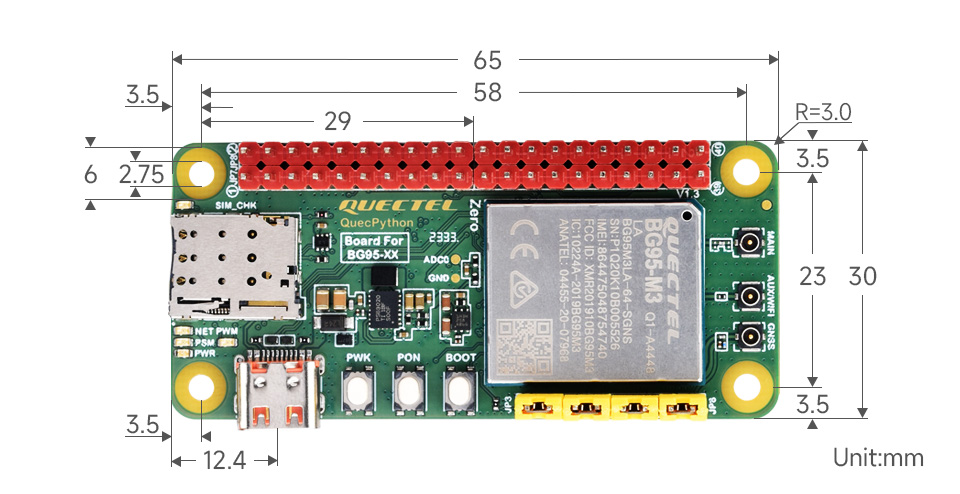
Dimensions: About 65 x 30mm (Raspberry Pi Zero form factor)
Waveshare offers the Quectel BG95-M3 Zero SBC for $65.31 on Aliexpress and around $70 on Amazon. They also sell larger QuecPython and Raspberry Pi HAT-compatible boards, including the “EC200U-EU C4-P01″ for regions like Europe, the Middle East, Africa, Australia, New Zealand, and Brazil, and the “EC200U-AU” for Australia and Latin America. You can also buy the modules directly from Waveshare for $54.99, but that does not include shipping.
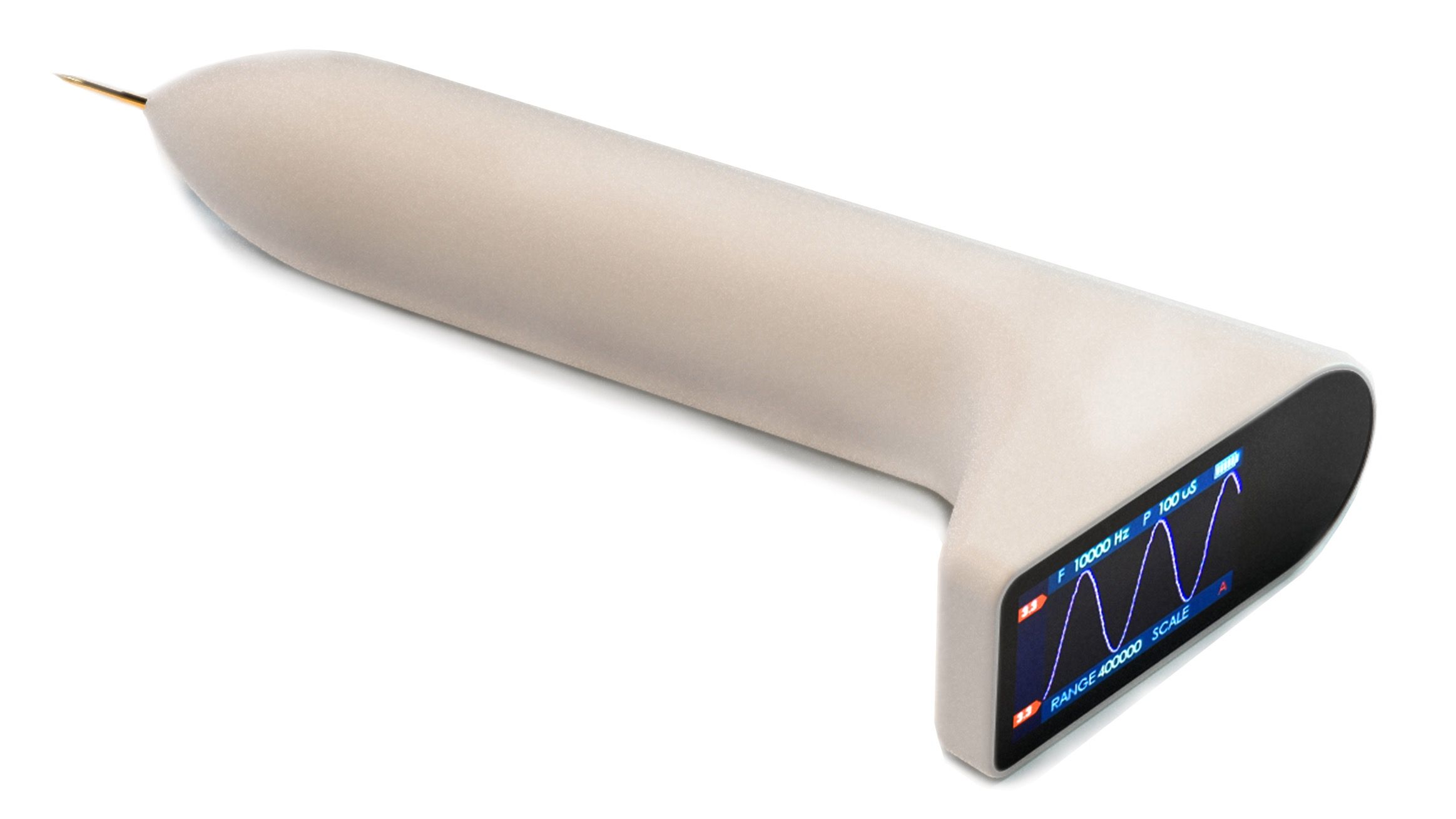
While looking for interesting and new products on the crowdfunding website I stumbled upon QUARK, An Arduino-based open-source multitool with a color LCD and a touchscreen display based on an ESP32 WiFI & Bluetooth wireless SoC.
The tool is a signal generator and oscilloscope, which the company compares to DT71 smart tweezers which do not have an oscilloscope function due to the tiny display. multitool is your go-to solution for electronics measurements and analysis. With the ability to measure voltage (0-26 V), current (0-3.2 A), resistance (0-2 MΩ), capacitance (2 pf-1000 uF), inductance (up to 1 H), and much more.
QUARK will be an open-source hardware device, with firmware written in the Arduino IDE for easy user updates. It utilizes Bluetooth for smartphone connectivity, with no WiFi option available. Additionally, data retrieval is possible via a USB connection.
SMD & Color code display – Provides component information conveniently
UART Logging – Includes auto baud rate detection and plotting for data analysis
Signal Generator – Useful for testing and circuit development
User Interface:
USB Type-C – For both power and data transfer
Function button & touch control – Offers intuitive navigation
Power:
5V USB Type-C charging.
700mA internal battery – Enables up to 5 hours of portable operation.
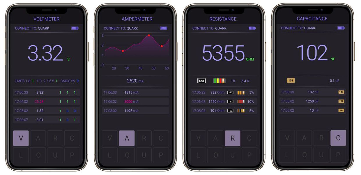
Two similar apps have been created for the QUARK platform. The first app, built using AppInventor, targets Android devices and is designed with beginner developers in mind. It’s a great way to learn the basics of app development. The second app, developed with the Flutter framework, offers a wider reach as it works on both Android and iOS devices.
The QUARK Arduino-based wireless multitool was successfully funded on Crowd Supplybut later on was canceled. Priced at $150, the reward included the fully assembled device with enclosure, a USB-C probe, and a carrying case.