Closed Loop Analog Position Control using Brushed DC Motor and Potentiometer

The project presented here is a low-cost position control closed-loop analog-servo using brushed DC motor and potentiometer as feedback. This project provides all necessary active functions for a closed-loop servo system using a Brushed DC Motor and potentiometer mounted on the output shaft of the DC Motor with Gear. The project is ideally suited for almost any servo positioning application. Can be used in applications such as side mirror movement control for cars, car head lamp beam control, animatronics, robotics, etc.

Closed Loop Analog Position Control using Brushed DC Motor and Potentiometer – [Link]

BQ27220 – Single cell pack/system-side CEDV battery fuel (gas) gauge w/pre-programmed chemistry profiles

The Texas Instruments bq27220 battery fuel gauge is a single-cell gauge that requires minimal user configuration and system microcontroller firmware development, leading to quick system bring-up. The bq27220 device uses the Compensated End-of-Discharge Voltage (CEDV) algorithm for fuel gauging and provides information such as remaining battery capacity (mAh), state-of-charge (%), runtime-to-empty (min), battery voltage (mV), temperature (°C), and state-of-health (%).

The bq27220 battery fuel gauge has ultra-low power consumption in NORMAL (50 μA) and SLEEP (9 μA) modes, leading to longer battery runtime. Configurable interrupts help save system power and free up the host from continuous polling. Accurate temperature sensing is supported via an external thermistor.

Customers can use preloaded CEDV parameters in ROM or can generate custom chemistry parameters using TI’s web-based tool, GAUGEPARCAL. Custom-generated parameters can be either programmed in the device RAM by the host on power up of the system or customers can program the parameters to an onboard One-Time Programmable (OTP) memory.

Battery fuel gauging with the bq27220 device requires connections only to PACK+ (P+) and PACK– (P–) for a removable battery pack or embedded battery circuit. The tiny, 9-ball, 1.62 mm × 1.58 mm, 0.5-mm pitch NanoFree™ chip scale package (DSBGA) is ideal for space-constrained applications.

Features

  • Single-Cell Li-Ion Battery Fuel Gauge
    • Resides in Pack or on System Board
    • Supports Embedded or Removable Batteries
    • Powers Directly from Battery with Integrated LDO
    • Supports a Low-Value (10-mΩ) External Sense Resistor
  • Ultra-Low Power Consumption in NORMAL (50 µA) and SLEEP (9 µA) Modes
  • Battery Fuel Gauging Based on Compensated End-of-Discharge Voltage (CEDV) Technology
    • Reports Remaining Capacity and State-of-Charge (SOC) with Smoothing Filter
    • Adjusts Automatically for Battery Aging, Self-Discharge, Temperature, and Rate Changes
    • Provides Battery State-of-Health (Aging) Estimation
  • Microcontroller Peripheral Supports:
    • 400-kHz I2C™ Serial Interface
    • Configurable SOC Interrupt OR Battery Low Digital Output Warning
    • Internal Temperature Sensor OR Host-Reported Temperature OR External Thermistor

Application Diagram

more information: https://www.ti.com/product/BQ27220

MAX16054 – On/Off Controller with Debounce and ±15kV ESD Protection

The is a pushbutton on/off controller with a single switch debouncer and built-in latch. It accepts a noisy input from a mechanical switch and produces a clean latched digital output after a factory-fixed qualification delay. The MAX16054 eliminates contact bounce during switch opening and closing. The state of the output changes only when triggered by the falling edge of the debounced switch input; the output remains unchanged on the rising edge of the input. Robust switch inputs handle ±25V levels and are ±15kV ESD protected for use in harsh industrial environments. The MAX16054 features a complementary output, OUT, which is the inverted state of OUT. An asynchronous CLEAR input allows an external signal to force the output flip-flop low. Undervoltage-lockout circuitry ensures that OUT is in the off state upon power-up. The MAX16054 requires no external components, and its low supply current makes it ideal for use in portable equipment. The MAX16054 operates from to +5.5V single supply. The MAX16054 is offered a 6-pin thin SOT23 package and operates over the to +125°C automotive temperature range.

Key Features

  • Robust Inputs Can Handle Power Supplies Up to ±25V
  • ±15kV ESD Protection
  • Latched Output
  • Low 7µA Supply Current
  • Operates from 2.7V to 5.5V
  • -40°C to +125°C Temperature Range
  • Thin SOT23 Package

more information: https://www.maximintegrated.com/en/products/power/supervisors-voltage-monitors-sequencers/MAX16054.html

SRC0 – Smart push-button on/off controller with Smart Reset and power-on lockout

The SRC0 devices monitor the state of connected push-button(s) as well as sufficient supply voltage. An enable output controls power for the application through the MOSFET transistor, DC-DC converter, regulator, etc. If the supply voltage is above a precise voltage threshold, the enable output can be asserted by a simple press of the button. Factory-selectable supply voltage thresholds are determined by highly accurate and temperature-compensated references. An interrupt is asserted by pressing the push-button during normal operation and can be used to request a system power-down. The interrupt is also asserted if undervoltage is detected. By a long push of one button (PB) or two buttons (PBand SR) either a reset is asserted or power for the application is disabled depending on the option used. The device also offers additional features such as precise 1.5 V voltage reference with very tight accuracy of 1%, separate output indicating undervoltage detection and separate output for distinguishing between interrupt by push-button or undervoltage.
The device consumes very low current of 6 μA during normal operation and only 0.6 μA current during standby.

The SRC0 is available in the TDFN12 package and is offered in several options among features such as selectable threshold, hysteresis, timeouts, output types, etc.

Features

  • Operating voltage 1.6 V to 5.5 V
  • Low standby current of 0.6 μA
  • Adjustable Smart Reset™ assertion delay time driven by external CSRD
  • Power-up duration determined primarily by push-button press
  • DebouncedPBand SRinputs
  • PBand SRESD inputs withstand voltage up to ±15 kV (air discharge) ±8 kV (contact discharge)
  • Active high or active low enable output option (ENor EN) provides control of MOSFET, DC-DC converter, regulator, etc.
  • Secure startup, interrupt, Smart Reset™or power-down driven by push-button
  • Precise 1.5 V voltage reference with 1% accuracy
  • Industrial operating temperature -40 to +85 °C
  • Available in TDFN12 2 x 3 mm package

Application Circuit

more information: https://www.st.com/en/reset-and-supervisor-ics/src0.html

STMicroelectronics STM66xx Smart Push-Button On / Off Controller

STMicroelectronics STM6600/STM6601 Smart Push-Button On / Off Controllers with Smart Reset™ and power-on lockout protects against the hazards faced by battery-operated devices. These types of devices include smartphones, digital cameras, and media players. The STM6600/STM6601 controllers enable and disable power for the application depending on push-button states, signals from the processor, and battery voltage. If the battery is excessively discharged or a fault is detected in the power supply, the IC blocks power-up. These devices also implement smart-reset capabilities to enable users to safely recover gadgets that have frozen or crashed during normal operation. The STM6600/STM6601 controllers connect directly to the power and reset buttons and have circuitry to prevent external interference such as electrostatic discharges. These devices feature a very low current consumption of 6µA in normal operation and only 1µA during standby, resulting in virtually no battery drain when the application is turned off.

Features

  • Operating voltage 1.6V to 5.5V
  • Low standby current of 1μA
  • Adjustable smart reset assertion delay time driven by external CSRD
  • Power-up duration determined primarily by push-button press (STM6600) or by fixed time period, tON_BLANK (STM6601)
  • Debounced PB and SR inputs
  • PB and SR ESD inputs withstand voltage up to ±15kV (air discharge) ±8kV (contact discharge)
  • Active high or active low enable output option (EN or EN) provides control of MOSFET, DC-DC converter, regulator, etc.
  • Secure startup, interrupt, smart reset or power down driven by push-button
  • Precise 1.5V voltage reference with 1% accuracy

Block Diagram

Application Circuit

more information: https://www.st.com/en/reset-and-supervisor-ics/stm6600.html

Chhavi – Ultra-Low-Power Fingerprint Sensor Featuring ESP32 SoC

Recent time has shown an increase in the number of fingerprint sensors and modules available in the Tech ecosystem following the need for physical security and biometric authentication for device and personnel management. One of the most recent is the new device by a hardware design company based in India – Chhavi.

Chhavi by Vicharak is a dense, wireless, touch-capacitive sensor built on ESP32 MCU with Wi-Fi and Bluetooth capabilities as well as an optional NFC features. It is based on open source code compatible with Arduino and has an FPC BM-Lite fingerprint sensor from Fingerprint which provides enhanced biometric performance in terms of accuracy and low power demand compared to optical fingerprint sensors.

Chhavi is built to meet ultra-low-power applications and high-end security requirements. The NFC feature of Chhavi is provided to solve the problem of high-quality fingerprint sensor requirements of most authentication and locking systems. There’s also an optional battery to support battery-based and mobile systems although it can be powered through a USB port.

The fingerprint sensor is further equipped with a vibration motor that can provide haptic feedback in applications such as notification of successful or unsuccessful user interface – scan. There’s also a self-generating or programmable ON/OFF switch that allows users to monitor and preserve power when the board is draining off a battery. This programmable switch can also function as a GPIO interface when the device is USB powered.

Features and Specifications Include:

Physical Features:

  • 26 x 26 x 9 mm (without battery)
  • 1x MCU reset button
  • 1x power-switch (user-configurable)
  • Vibration motor for haptic feedback

Processing:

  • 32-bit ESP32 dual-core processor operating at 240 MHz
  • 4 MB SPI flash

Connectivity:

  • CP2102 USB-to-UART converter for serial programming
  • I²C interface via PN7150

Power Management:

  • 600 mA, 3.3 V LDO regulator
  • LiPo battery management
  • Support for 250 – 500 MAh LiPo batteries
  • Capacitive finger-detection that allows for deep sleep when not in use
  • Optimized power path for low-power battery usage
  • Battery voltage-level detection
  • Power (red) & charge (orange) LEDs
  • Supply-voltage supervisor that can power down MCU when battery power is low
  • ESD protection on the USB data bus
  • Over-voltage protection (OVP) for USB power
  • Over-current protection (OCP) for USB power

Fingerprint Sensor:

  • FPC BM-LITE Module (99% accurate fingerprint sensing)
  • Automatic finger detection
  • Protective sensor coating is resistant to scratches and electrostatic discharge (ESD)
  • One-to-one verification mode
  • Front side IP rating: IPX7
  • Durability: 10 million finger placements
  • Scratch resistance (pencil hardness): 4H
  • Sensor matrix: 160 x 160 pixels
  • Number of pixels: 25,600 pixels
  • Active sensing area: 8 x 8 mm

Wireless:

  • 2.4 GHz 802.11 b/g/n Wi-Fi via ESP32
  • Bluetooth BLE 4.2 via ESP32
  • (Optional) 13.56 MHz NFC
  • 3D antenna

NFC Specifications & RF Protocols:

  • PN7150 NFC controller
  • NFCIP-1  & NFCIP-2
  • ISO/IEC 14443A, ISO/IEC 14443B PICC, and NFC Forum T4T modes via host interface
  • NFC Forum T3T via host interface
  • ISO/IEC 14443A, ISO/IEC 14443B PCD designed according to NFC Forum digital protocol T4T platform and ISO-DEP
  • FeliCa PCD mode
  • MIFARE Classic PCD encryption mechanism (MIFARE Classic 1K/4K)
  • NFC Forum tag 1 to 5 (MIFARE Ultralight, Jewel, Open FeliCa tag, MIFARE DESFire)
  • ISO/IEC 15693/ICODE VCD mode
  • Supports card emulation as well as reader mode

Chhavi’s software support allows flexibility, easy and out-of-the-box programming for makers and DIY users with the help of its inbuilt USB-to-UART adapter. And according to Vicharak, the development of a library for ESP-IDF framework users is also on the way. Vicharak also points to Github for Chhavi’s source files and fingerprint’s website for biometric sensor information.

As of the time of this writing, Chhavi is only available for crowdfunding on CrowdSupply at $49 (for only fingerprint sensor); $59 (for the fingerprint sensor and NFC); $59 (for the fingerprint sensor and battery), and, $69 (for the fingerprint sensor, NFC and battery). An additional $8 (US) or $18 (Worldwide) shipping fee applies to all four rewards.

The funding campaign is scheduled to end on Nov 18, 2021, at 03:59 pm PST (11:59 pm UTC) for manufacturing to commence immediately. To join the funding campaign, and get more information on Vicharak’s Chhavi, visit CrowdSupply.

Embedded AI platform combines 16-core NXP Layerscape LX2160A processor with up to 5x Hailo-8 NPUs

MicroSys Electronics, a world leader in embedded systems, has gone into partnership with Leading AI chipmaker, Hailo, to launch a scalable embedded platform for AI processing at the edge.

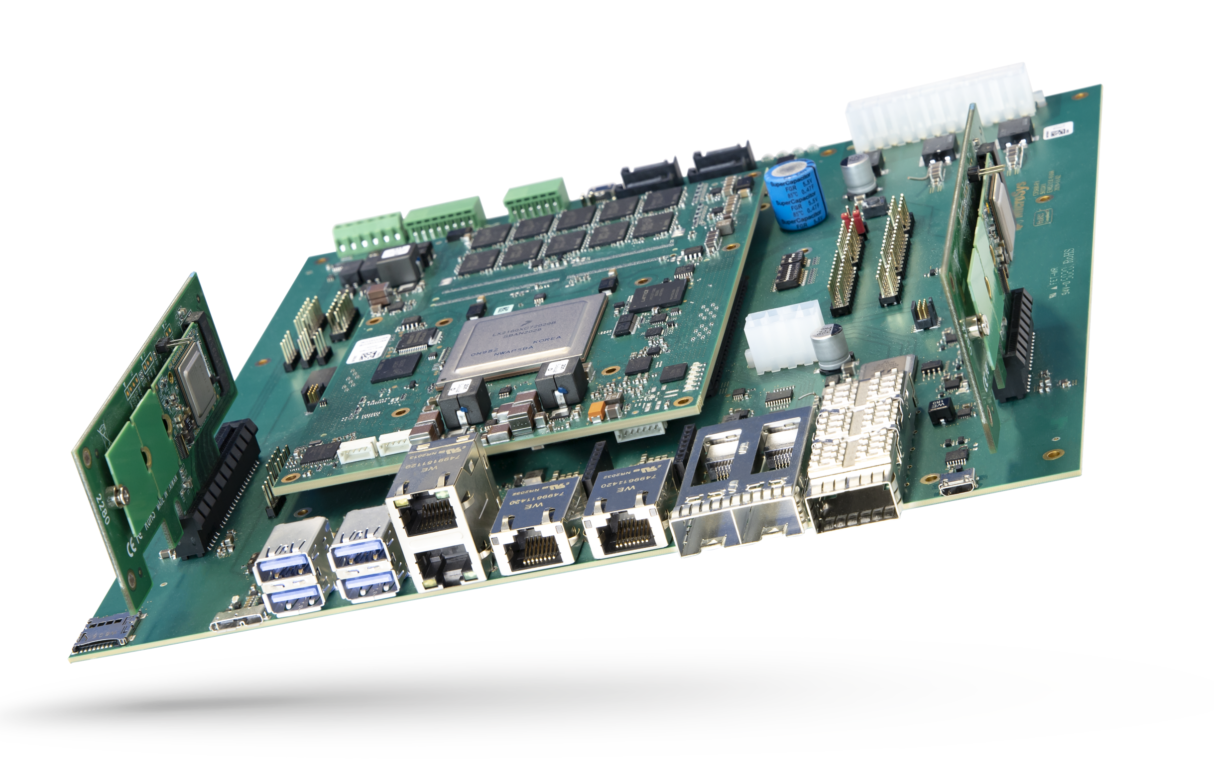
The company released a miriac® AIP-LX2160A dev kit with up to 5x integrated Hailo-8™ AI accelerator modules for processing performance up to 130 TOPS. They also released a miriac® MPX-LX2160A module which is used as a foundation for the kit.

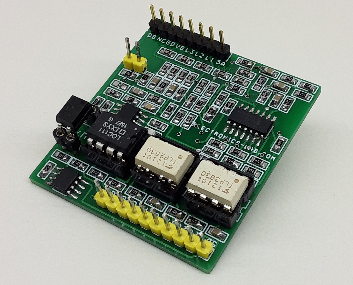
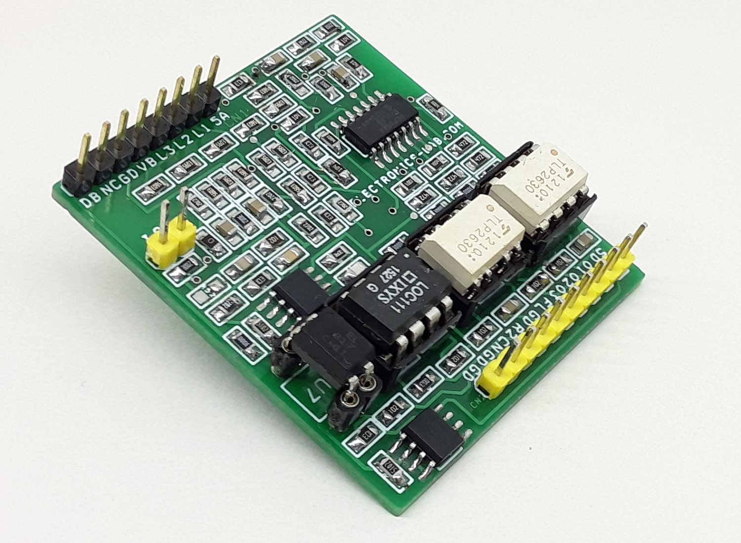
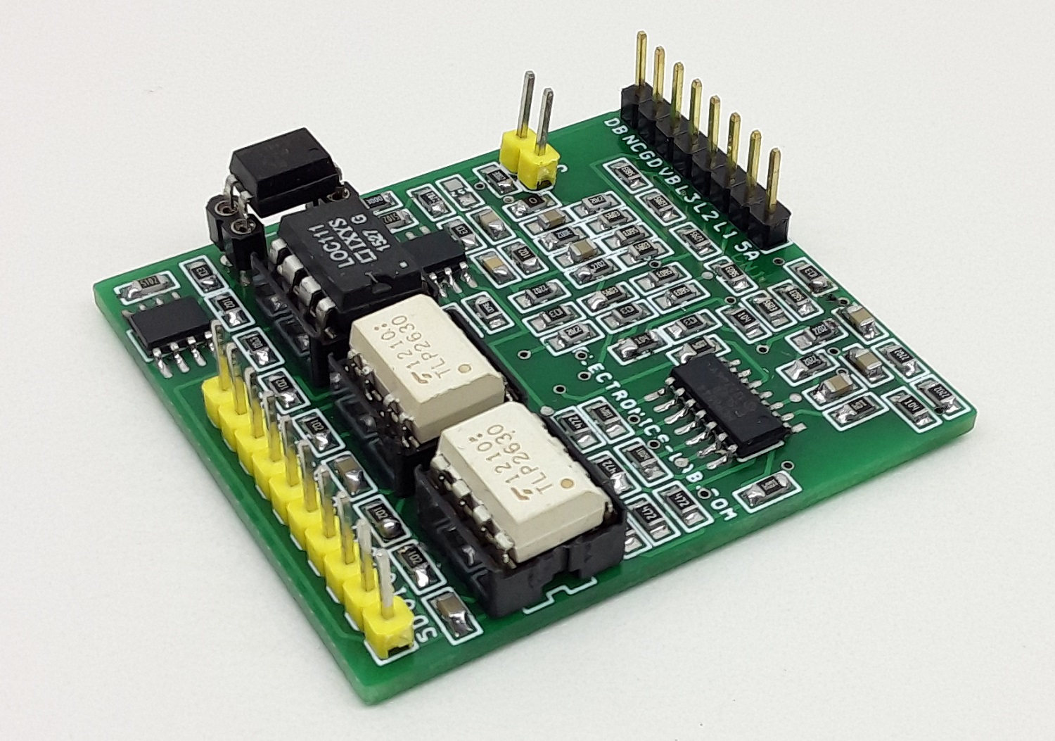
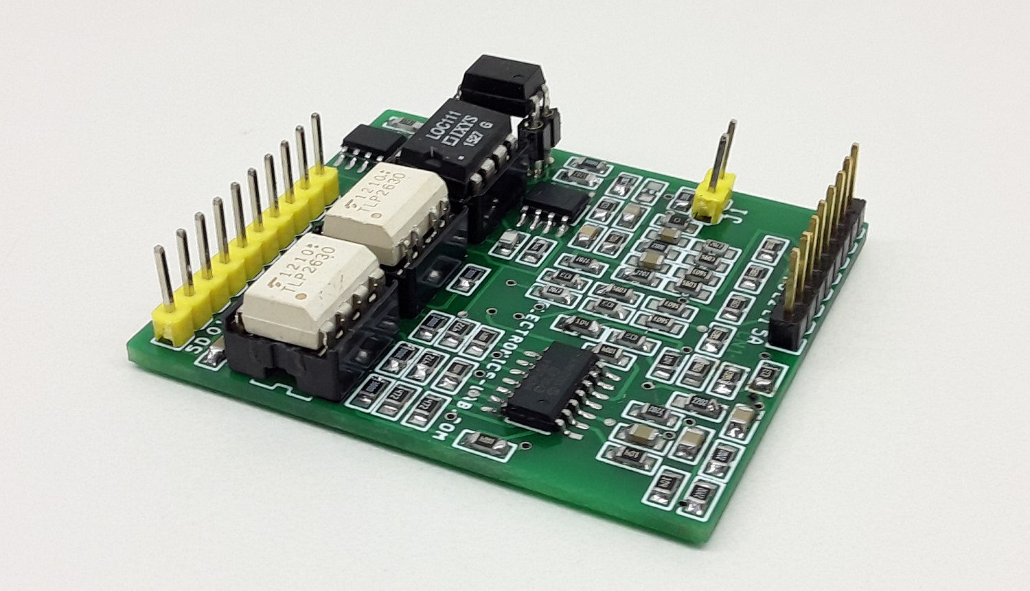
The AIP-LX2160A kit is equipped with 2x 25GbE, 2x 10GbE, 2x 1GbE ports as well as 16x PCIe lanes (PCIe x8, PCIe x4, and PCIe x4, each with 2.5, 5 or 8Gbps support). The dev kit also has 4x SATA III, 1x microSD, 4x USB 3.0 host, a micro-USB 3.0 OTG port, 3x serial ports (UART/USB console, TTL, and RS485) JTAG, FlexSPI, 2x I2C, 6x-in/6x-out SPS, 4x LEDs, temperature sensors, fan controller, boot select, an RTC, a 12V input and ATX power supply with a 200W minimum, and 0 ~ 80°C operating range.

The MPX-LX2160A module, on the other hand, runs Linux on NXP’s 16-core, Cortex-A72 Layerscape LX2160A, which we have seen on high-end networking boards. The module also offers 2 Gbits Octal SPI flash, 8GB to 256GB eMMC, and up to 128GB of DDR4.

Hailo’s Hailo-8 M.2 AI acceleration module for AI applications offers industry-leading AI performance for edge devices. The combination of the Hailo-8™ AI acceleration module and the Arm® Cortex® NXP® Layerscape® platforms offers the benefit of integrating highly efficient AI in connected edge appliances. According to MicroSys, the embedded platform is the first ever to deploy up to 5x Hailo-8 cards on a single device and the aim is to help users get the most out of AI and neural networks.

“Hailo’s AI processor allows edge devices to run full-scale deep learning applications more efficiently, effectively, and sustainably while significantly lowering costs. In combination with our NXP processor-based platforms, our customers get one of the most powerful AI solutions that can be developed for edge applications,”

says Managing Director at MicroSys Electronics.

Features:

  • 5x parallel Hailo-8 AI modules for massive processing performance up to 130 TOPS
  • Full Hailo-8 performance combined with maximum power efficiency (FPS / W ratio)
  • Up to 955 YOLOv5m / 6145 Resnet_v1_50 / 5200 Ssd_mobilenet_v1 object detection frames (416×416) per second performance
  • Hailo AI ecosystem incl. AI toolchain and developer tools
  • Deep learning pre-trained models for various computer vision tasks

Applications:

The high-performance application-ready AI platform is perfect for a wide range of applications in fields like Industry 4.0, automotive and heavy machinery. These include:

  • predictive maintenance
  • collaborative robotics,
  • video surveillance servers in systems with distributed cameras
  • communication servers for autonomous vehicles in logistics and agriculture
  • heavy equipment for construction, as well as,
  • edge servers in trains where multiple GigE Vision camera streams are analyzed with AI

There are no details on the price and availability of both the miriac AIP-LX2160A kit or miriac MPX-LX2160A module but further details may be found on the product page or the company’s announcement page.

Signal Conditioner for Sensorless BLDC Operations

This is a back EMF signal conditioning circuit that can be used to develop high-voltage sensorless motor drivers. When a sensorless algorithm is used to control the BLDC motor speed, the Back EMF (BEMF) signals are used. Based on zero crossing of BEMF signals, motor commutation is decided in the firmware. The signal conditioning circuit has mainly three blocks: the first is a low-pass filter for each phase voltage the second is a comparator circuit for determining the zero crosspoints and the third is a high-speed optocoupler. The optocoupler provides isolation between high-voltage motor driver circuitry and microcontroller.

Inputs

  • 3 Phase Signal inputs, from 3 Phase Motor connections
  • Current Feedback across the shunt resistor of IPM/IGBT Emitter
  • DC Bus Monitor, Over Voltage protection, 200V DC or 400V DC

Outputs

  • 3 Phase Digital Zero Cross Signals (Optically Isolated)
  • DC Bus Over Voltage, Normally High Output (Optically Isolated)
  • Current to Voltage Cycle by Cycle Output (Optically Isolated)
  • Optional Trip Optocoupler (Not Install, can be used, If current feedback circuit is not required)

Features

  • Supply 5V DC for Analog Side (Inputs)
  • Supply 5V DC For Digital Side (Outputs)
  • Detect the Back EMF of 3 Phase Motor and Provides 3 TTL Outputs
  • DC Bus Voltage Feedback Low or High TTL Output
  • Optional Current Sense Circuit provides Cycle by Cycle voltage output proportional to motor current
  • All outputs are optically Isolated, Frequency up to 20Khz
  • Jumper J1 – Overvoltage protection, 200V or 400V DC (Close the Jumper for 400V)
  • The project requires 2 separate 5V DC power supplies, Analog-Input side, and digital-Output side
  • PCB dimensions: 47.94 x 42.70 mm

BLDC Motor Winding and Back EMF

To run a BLDC motor without sensors, it is important to sense the rotor magnet position with reference to the windings on the stator. In order to do this properly, the Back EMF on the unexcited winding is monitored. As the motor is spun, the voltage waveform on the three winding phases will be seen. There are 6 sectors, each 60 degrees wide, which accumulate to give one 360-degree electrical revolution of the motor. In each sector, two windings are excited: one with a high voltage and the other with a low voltage. The third winding is not excited. As the rotor rotates from one sector to another, a new set of windings is excited. The sequence of excitation in each sector is provided by the motor manufacturer. The winding in each sector that is not excited will be influenced by the Back EMF voltage. This voltage is not high or low, but a falling or rising voltage level, going symmetrically from a high-to-low or a low-to-high. It crosses the center, or star point voltage, at about 30 degrees before the next commutation point of the rotor. This center, or star point voltage, is also referred to as the zero-crossing voltage. Its value is exactly half the voltage applied to the excited windings of the motor. These signals can be interfaced to fast ADV to sense the zero-crossing point. Having sensed the zero-cross point, it can predict the time required for the next commutation phase.

The board takes signals from 3 motor connections and provides isolated 5V TTL signal which can be further interfaced to a microcontroller or DSP. Board can take direct inputs from high-voltage 180V or 330V DC, AC IPM modules, or 3 phase MOSFET/IGBT-based inverters. This board can be modified to be used with lower voltage motor drivers, calculate the input divider resistors value as per motor voltage.

Current Feedback (IC U4, U5, U6) – Optional Do Not Populate

Optional current to voltage circuit can help to measure the current of IPM module or 6 IGBT/MOSFET inverter, the block measures the current across the shunt resistors and provides a proportional voltage output, this output is optically isolated. This block is created using U4, U5, U6 chips, Gain can be set using R54. The circuit provides near-zero output when a current is not flowing, otherwise, the output is 3V/Amp.

Bus Voltage Feedback/Over Voltage Fault (Op-Amp U1D)

The DC bus voltage is attenuated using a voltage divider and compared with a fixed reference signal using an external comparator. On the board, when jumper J1 is open, the overvoltage is set to 200V on the DC bus. If jumper J1 is shorted, then the overvoltage limit is 400V. The Fault FL pin is used to monitor the overvoltage condition. Normally FL pin is low, goes high when overvoltage condition occurs.

Credits: Reference Microchip Application Notes

Schematic

Parts List

NOQNTY.REFDESC.MANUFACTURERSUPPLIERPART NO
11CN16 PIN MALE HEADER PITCH 2.54MMWURTHDIGIKEY732-5319-ND
21CN210 PIN MALE HEADER PITCH 2.54MMWURTHDIGIKEY732-2670-ND
31CN32 PIN MALE HEADER PITCH 2.54MMWURTHDIGIKEY732-5315-ND
47C1 to C70.1uF/50V SMD SIZE 0805MURATA/YAGEODIGIKEY
51C84K7PF/50V SMD SIZE 0805MURATA/YAGEODIGIKEY
61C933PF/50V SMD SIZE 0805MURATA/YAGEODIGIKEY
71C10100PF/50V SMD SIZE 0805MURATA/YAGEODIGIKEY
81J12 PIN MALE HEADER PITCH 2.54MMWURTHDIGIKEY732-5315-ND
94R1,R14,R24,R364K7 5% SMD SIZE 0805MURATA/YAGEODIGIKEY
104R2,R13,R15,R25100K 5% SMD SIZE 0805MURATA/YAGEODIGIKEY
114R3,R16,R26,R381M 5% SMD SIZE 0805MURATA/YAGEODIGIKEY
125R4,R17,R27,R37,R5510K 5% SMD SIZE 0805MURATA/YAGEODIGIKEY
135R5,R6,R33,R34,R491K 5% SMD SIZE 0805MURATA/YAGEODIGIKEY
1412R7,R10,R11,R18,R19,R22560K 1% SMD SIZE 0805MURATA/YAGEODIGIKEY
R28,R30,R31,R40,R41,R42560K 1% SMD SIZE 0805MURATA/YAGEODIGIKEY
156R8,R12,R20,R23,R32,R3522K 1% SMD SIZE 0805MURATA/YAGEODIGIKEY
164R9,R21,R29,R44300E 1% SMD SIZE 0805MURATA/YAGEODIGIKEY
171R390E SMD SIZE 0805MURATA/YAGEODIGIKEY
182R43,R4727K 1% SMD SIZE 0805MURATA/YAGEODIGIKEY
192R45,R4630K 1% SMD SIZE 0805MURATA/YAGEODIGIKEY
201R48360E 1% SMD SIZE 0805MURATA/YAGEODIGIKEY
211R50470E 1% SMD SIZE 0805MURATA/YAGEODIGIKEY
222R51,R5351K 1% SMD SIZE 0805MURATA/YAGEODIGIKEY
235U7,R52,R56,R57,R58DNPOPTIONAL
241R5420K 1% SMD SIZE 0805MURATA/YAGEODIGIKEY
251U1MCP6544MICROCHIPMOUSER579-MCP6544-E/SL
262U2,U3TLP2630/VO2630VISHAYMOUSER782-VO2630
272U4,U5MCP6002 OR LM358MICROCHIPDIGIKEYMCP6002-E/SN-ND
281U6LOC111/SMIXYSDIGIKEYCLA116-ND

Connections

Block Diagram

Gerber View

Photos

Video

LOC111 Datasheet

4-Channel Remote Receiver Using NRF24L01 Radio Module – Arduino Compatible

Controlling 4 devices using an RF remote is very easy with this project. This is an Arduino compatible project. NRF24L01 module, Atmega328 microcontroller, 3.3V regulator, and few other components are part of the project. Onboard power LED and an additional functional LED is provided. The project provides 4x TTL outputs that can be interfaced with a relay board, solid-state relay boards, motor drivers, and other projects.  The circuit works with 5V DC and requires a few milliamps current. D2 Power LED, D1 optional function LED.

Compatible 4 Channel RF Transmitter

This receiver board is compatible with the 4 Channel RF Remote Transmitter using nRF24L01- Arduino Compatible previously published on our website.

Please refer to the example application diagram below to interface the receiver board with Low Profile 2 Channel Solid State Relay for AC Loads which helps you to drive 2x high voltage loads with 230V AC input. You can use 2x boards for 4 channels control.

Arduino Pins

  • Output 1: Digital Pin D2
  • Output 2: Digital Pin D3
  • Output 3: Digital Pin D4
  • Output 4: Digital Pin D5
  • LED D1 >> Digital Pin D6

NDRF24L01 Transceiver Module

  • CE>> Digital pin D9
  • CSN>> Digital pin D10
  • MOSI>> Digital pin D11
  • MISO>> Digital pin D12
  • SCK>> Digital pin D13
  • IRQ>> Digital pin D8
  • 3V and GND

Features

  • Operating Supply 5V DC, Consumes 20mA Current
  • 4 x TTL Outputs, Easy Interface with Relay Board, Solid State Relay Board
  • Controlling Lights, Fans, Robots is very easy
  • PCB Dimensions 37.47x 36.83 mm

Arduino Code for the Transmitter and Receiver is available below, download the code and upload it to ATmega328 microcontroller, more info is available here:

https://www.arduino.cc/en/Tutorial/BuiltInExamples/ArduinoToBreadboard

The receiver board is compatible with the following boards:

AC Solid State Relay Board

DC Solid State Relay Board

Relay Board (This board has 12V Relay, replace with 5V Relay for single Supply 5V operation or use 5V for Receiver, 12V for Relay Board)

Schematic

Parts List

NO.QNTY.REF.DESCMANUFACTURERSUPPLIERSUPPLIER PART NO
11CN14 PIN MALE HEADER PITCH 2.54MMWURTHDIGIKEY732-5317-ND
21CN26 MALE HEADER PITCH 2.54MMWURTHDIGIKEY732-5319-ND
31CN3NRF24L01SEEDSTUDIODIGIKEY1597-1352-ND
42C1,C222PF/50V SMD SIZE 0805MURATA/YAGEODIGIKEY
53C3,C4,C50.1uF/50V SMD SIZE 0805MURATA/YAGEODIGIKEY
62C6,C710uF/16V SMD SIZE 1206MURATA/YAGEODIGIKEY
72D1,D2LED RED SMD SIZE 0805OSRAMDIGIKEY475-1278-1-ND
81R11M 5% SMD SIZE 0805MURATA/YAGEODIGIKEY
92R2,R3220E 5% SMD SIZE MURATA/YAGEODIGIKEY
101R410K 5% SMD SIZE 0805MURATA/YAGEODIGIKEY
111U1ATMEGA328MICROCHIPDIGIKEYATMEGA328-PU-ND
121U2LM1117-3.3VTIDIGIKEYLM1117MP-3.3/NOPBCT-ND
131Y116MHZECS INCDIGIKEYX1103-ND

Connections

Example Application

Gerber View

Photos

Video

ATmega328 Datasheet

LinkSwitch-TNZ Switching Power Supply IC

Power Integrations’ switching IC saves 60% of standby power in smart home products

With integrated lossless AC zero-cross detection, Power Integrations’ LinkSwitch-TNZ ICs provide best-in-class light load efficiencies, enabling more system features to be powered in standby while still meeting stringent standby regulations. At the same time, component count is reduced by more than 40% compared to discrete designs.

Optionally, an X-capacitor discharge function can be included for high-power applications, leading to greater PCB space reduction, low BOM count, and increased reliability (LNK331x). Eliminating the bleed resistors required to meet IEC62368-1 can reduce no-load consumption in white goods by up to 1 W.

LinkSwitch-TNZ switching power supply ICs enable ±3% regulation across line and load, no-load consumption of less than 30 mW with external bias, and have an IC standby current of less than 100 µA.

Features

  • Lossless zero-cross detection and signal generation
  • Optional X-capacitor discharge function
  • Supports buck, buck-boost, and flyback topologies
  • Selectable device current limit
  • Reduces size and cost of magnetics and output capacitor
  • Allows the use of low-cost off-the-shelf inductors
  • Frequency jittering reduces EMI
  • 725 V MOSFET rating for excellent surge withstand
  • Comprehensive safety and reliability features
  • <150 µA leakage in 2-wire no neutral designs
  • No-load consumption <30 mW with external bias
  • Easily meets all global energy efficiency regulations

more information: https://www.power.com/products/linkswitch/linkswitch-tnz/lnk3304d

TOP PCB Companies