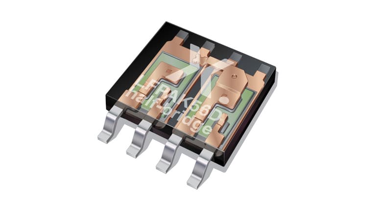
A series of half-bridge (high side & low side) MOSFETs constructed in the space-saving LFPAK56D package format. Occupying 30% lower PCB area compared to dual MOSFETs for 3 phase motor control topologies due to the removal of PCB tracks whilst permitting simple automated optical inspection (AOI) during production. The LFPAK56D half-bridge utilizes existing high volume LFPAK56D assembly processes, with proven automotive reliability. The package format uses flexible leads to improve overall reliability, and an internal copper clip connection between the MOSFETs simplifies PCB designs and brings a plug-and-play style solution with exceptional current handling capability.
Key features
60% lower parasitic inductance due to internal clip connection
30% space saving on PCB compared to LFPAK56D dual
High performance ID max >60 A
Low thermal resistance
Flexible leads for BLR
Footprint compatible with LFPAK56D dual
External leads for easy AOI
Beyond AEC-Q101 for automotive products
Applications
Handheld power tools, portable appliance and space constrained applications
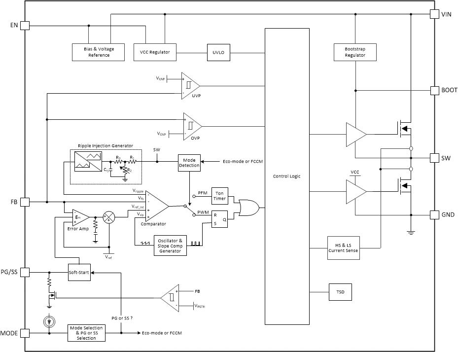
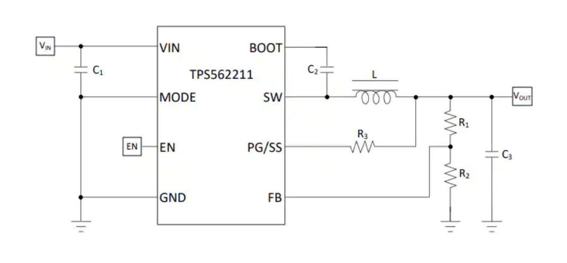
Texas Instruments TPS562211 2A Synchronous Buck Converter is a flexible, cost-effective solution in a SOT583 package. The TPS562211 Converter features a selectable Eco-mode operation or FCCM (Force Continuous Conduction Mode) operation. Furthermore, a selectable Power-Good indicator or external soft-start is also configurable through the MODE pin. The TPS562211 allows power sequencing by configuring Enable, Power-Good indicator, or external soft-start correctly. A 4.2V to 18V wide input voltage range supports a wide variety of common input rails, such as 12V and 15V. The device supports up to 2A continuous output current at output voltages between 0.6V and 7V.
The TI TPS562211 2A Synchronous Buck Converter implements a fast transient response with true fixed switching frequency using the Advanced Emulated Current Mode (AECM) control topology. Facilitating an internal smart loop bandwidth control, the TPS562211 provides a fast transient response over a wide output voltage range without the need for external compensation.
A cycle-by-cycle current limit on the high-side peak current protects the Converter in overload situations. This feature is enhanced by a low-side valley current limit, which prevents current runaway. Hiccup mode is triggered under overvoltage protection (OVP), undervoltage protection (UVP), UVLO protection, and thermal shutdown.
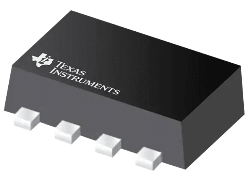
The TPS562211 2A Synchronous Buck Converter is housed in a 1.6mm × 2.1mm SOT583 package.
Features
4.2V to 18V Input voltage
0.6V to 7V Output voltage
Up to 2A continuous output current
45ns Minimum switching on time
98% Maximum duty cycle
High efficiency
Integrated 66mΩ and 33mΩ MOSFETs
Quiescent current 120μA typical
Highly flexible and easy to use
Selectable Eco-mode or FCCM operation
Selectable power good indicator or external soft start
Precise enable input
High accuracy
±1% (25°C) Reference voltage accuracy
±8.5% Switching frequency tolerance
Small solution size
Internal compensation for ease of use
SOT583 package
Minimum external components
Cycle-by-cycle current limit for both high-side and low-side MOSFETs
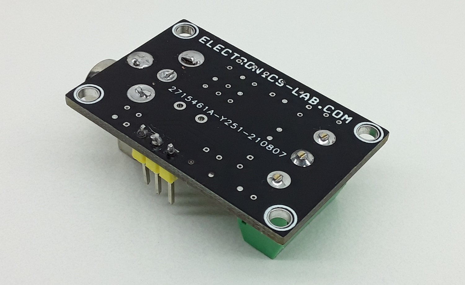
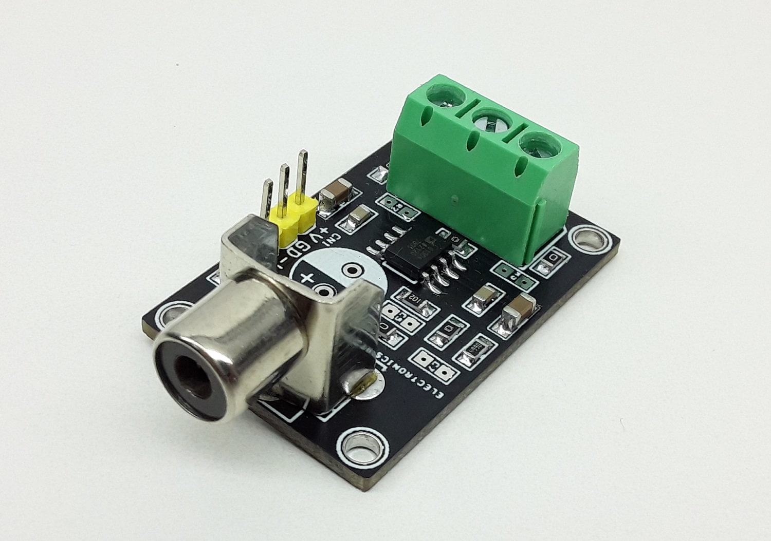
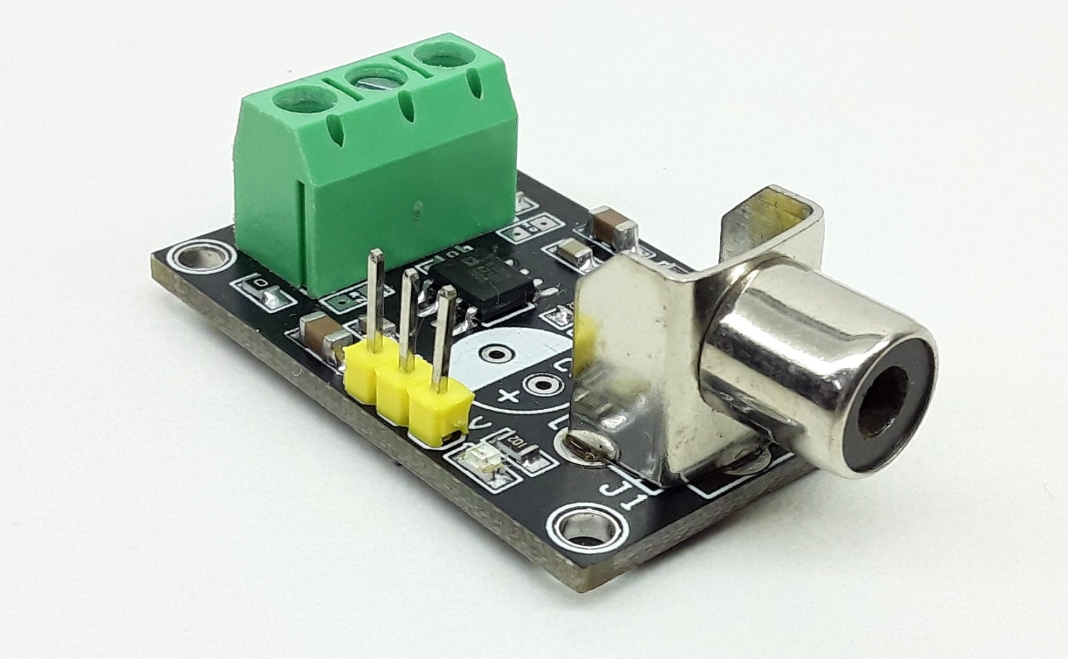
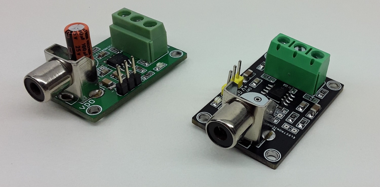
Stereo finds widespread applications in audio media production owing to the growing demand for portable consumer electronics and listening systems like PA systems and sound boxes supporting impression and sonics of natural hearing. Form factor requirement of the new maker and DIY boards and means reduced hardwiring and system components. The Wave III – 2 channel stereo audio player/recorder module manufactured by Senior Electron LLC is built to meet these specification requirements.
The module is furnished with FAT file system support which makes it compatible with multi-alarm voices, music players, and audio recorder applications. Its FAT file system allows users to play or create a file to record by calling file names using AT – commands. The wave III can record audio files on micro-SD and play pre-loaded files with 2 channel stereo of 10 – bits resolution.
It is equipped with an auto-baud rate detection system to automatically detect, adjust and assign baud rates up to 256 kbps for UART serial port communication. The module supports a standard serial RX/TX port for interfacing with devices like Arduino, Raspberry Pi, and microcontrollers. As a plus, it requires just a few plugs; power, audio in, and audio out to reduce overall system components.
From PCB reads, the board has 1 audio in and 1 audio out, which can only suggest that it runs a pseudo-stereo protocol. And that means it will not only offer reduced internal/control system components requirements but reduced external inputs peripherals too: only one microphone and one speaker is required for its 2-channel audio play/record function. This design also means that users don’t have to go through the headache of setting two microphones/speakers at orientations that will support sound localization of human perception. It’s just a plug-and-use architecture, a reason it should be the maker’s favorite.
Wave III also supports low latency commands allowing for playing multiple audio files without interruption, super high audio quality, and 8bit/16bit Wav audio formats. Its footprint, sample code, and documentation are available for Altium designers and Devkit solutions/users just to make using it a hitch-free task. The Devkit board has an in-built USB to UART FTDI chip, an audio I/O jack, and jumpers giving makers, DIYs, and hobbyists the flexibility of testing for suitable settings and functionalities. That’s a big plus too. Its sample code is fully written in C language and is compatible with Arduino and any other programmable devices and chips.
As at the time of this writing, the wave III with the manufacturer’s part name, Wave-3-RV2.0 is only available for an active funding campaign on GroupGets at a single-unit price of $25.00 and $65.00 for the Dev Kit, which the company says will help users to start working with the module straight up without having to design their own board.
“The Dev board has a USB to Uart FTDI chip on board, Audio input and output jack, and jumpers to try different settings. With this board, you can just easily plug a speaker or headphone to it and use a terminal to send commands to the module to play/record and try its different functionalities.”
Manufacturing will commence once the required target is reached according to the designer. Its campaign is scheduled to end on Sat, 06 Nov 2021, according to GroupGets.
To join the funding campaign, and get more information on Wave-3-RV2.0, visit GroupGets.
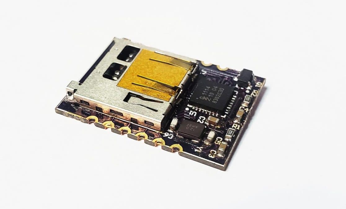
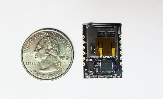
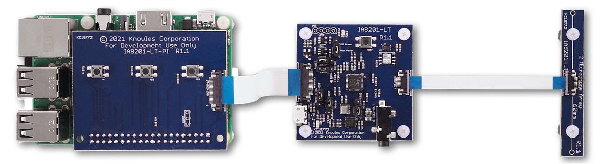
Knowles, has launched a development kit for the Raspberry Pi for prototyping products based on a homegrown AISonic IA8201 DSP that was introduced not long ago.
Designed to bring voice, audio edge processing, and machine learning (ML) listening capabilities to various systems, the devkit supports wake-on-voice processing for low latency voice UI, noise reduction, context awareness, and accelerated machine learning inferencing. It also supports
“high bandwidth processing of advanced, always-on contextually aware ML use-cases and memory for multiple algorithms,” says the company,
and offers a choice of 2 mic array boards with 2x or 3x mics respectively. There’s also an adapter board with three buttons connecting to the Raspberry Pi, as well as the DSP board itself connected via a flat cable to a microphone array.
Software support for the IA8201 SDK includes Amazon Alexa, Sensory, Retune, and Alango voice services. It also supports TensorFlow Lite Micro SDK for AI/ML applications. Configuration tools, firmware, algorithms, and other product briefs can all be accessed via the company’s Solutions Portal.
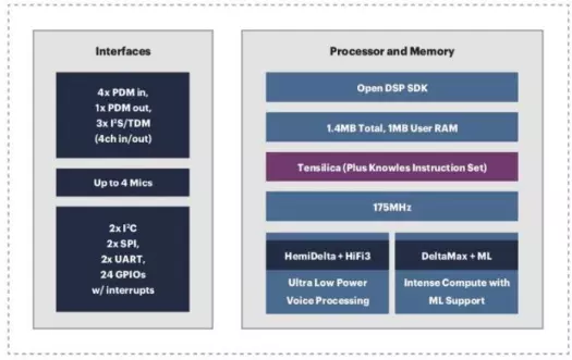
The Knowles’ AISonic IA8201 OpenDSP is aimed at lower-power AI processing. It features a Cortex-M4 chip along with 2x Tensilica-based, audio-centric DSP cores: a DeltaMax” Xtensa LX5 128-bit 4-way floating-point SIMD DSP core optimized for frame-based audio processing and DNN acceleration, and, a “HemiDelta” Xtensa LX5 64-bit 2-way floating-point SMID DSP core optimized for low power, always-on processing of sensor inputs.
Other features and specifications of the AISonic IA8201 DSP include:
1.44MB RAM (1MB is made available to the user)
Up to 4x PDM Digital Microphones – 1 stereo input, 4x mono inputs, and 1 stereo output (clock rates up to 6.144 MHz)
Up to 3x I2S/TDM ports supporting 8x 32-bit audio channels
SPI, I2C, UART, and GPIOs.
Up to 175 MHz clock speed
Voltage supply requirements
IA8201BC – 1.8V Vdd
IA8201CQ – 1.8V Vdd and 3.3V Vdd
Temperature Range: -20°C ~ 85°C
Packaging:
eWLB 3mm x 2.6mm x 0.715mm, 0.4 pitch, 42 ball (IA8201BC)
QFN 6.00mm x 6.00mm x 0.75mm, 0.5 pitch, 40 lead (IA8201CQ)
Usage for both the kit and the DSP includes smart home and building voice hubs applications, home entertainment systems, proximity detection systems, wireless earbuds, and inference engines for many industrial and commercial applications. You can also use it for security systems that detect glass breakage and for smoke alarms too.
The kit appears to be available for order but you may have to reach out to the company to get one as it is not being sold online. Other useful details on both the devkit and the IA8201 DSP can be found on the kit product page and datasheet respectively.
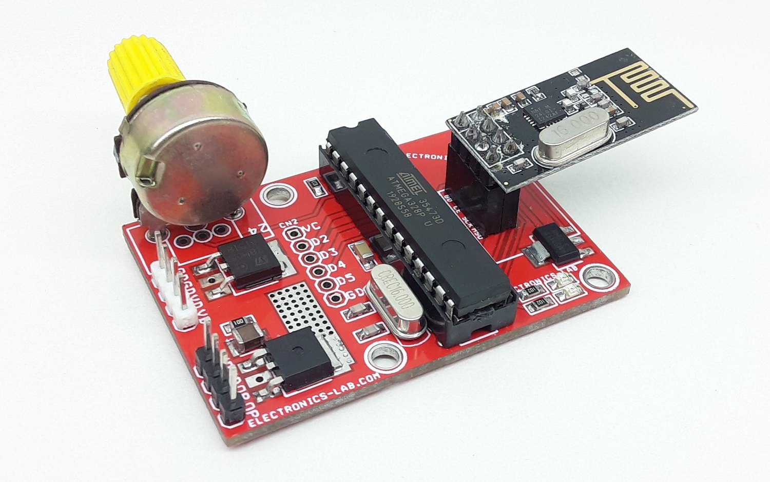
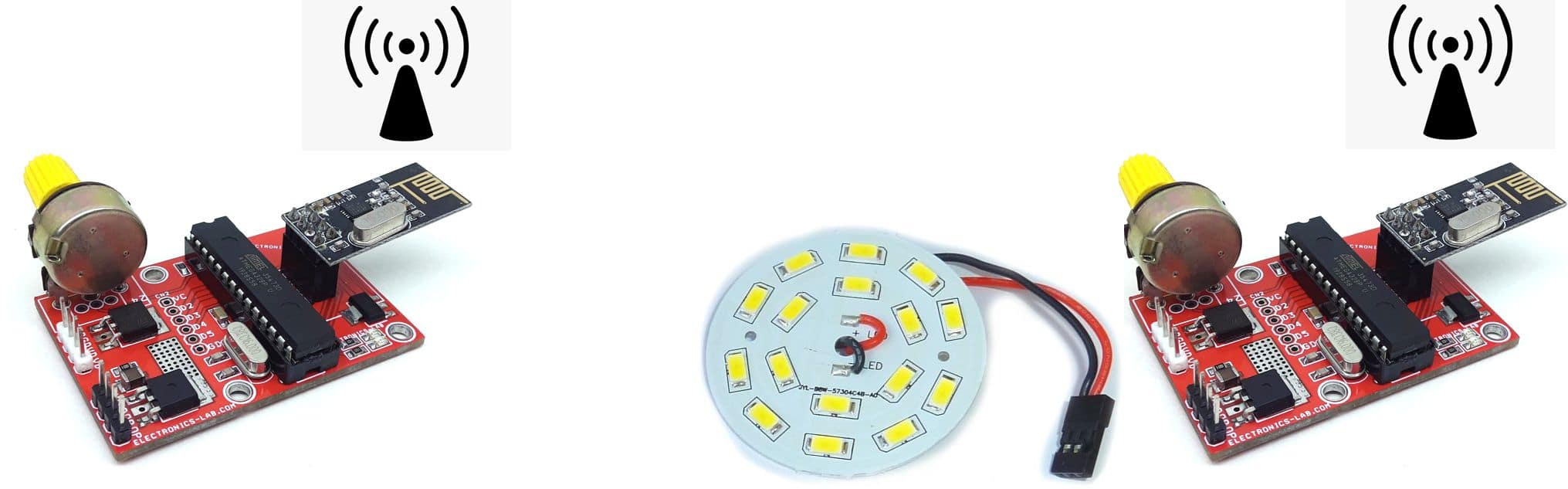
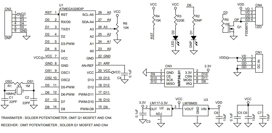
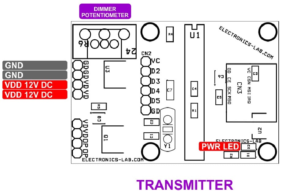
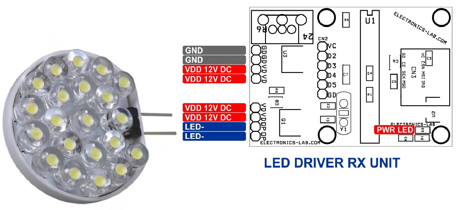
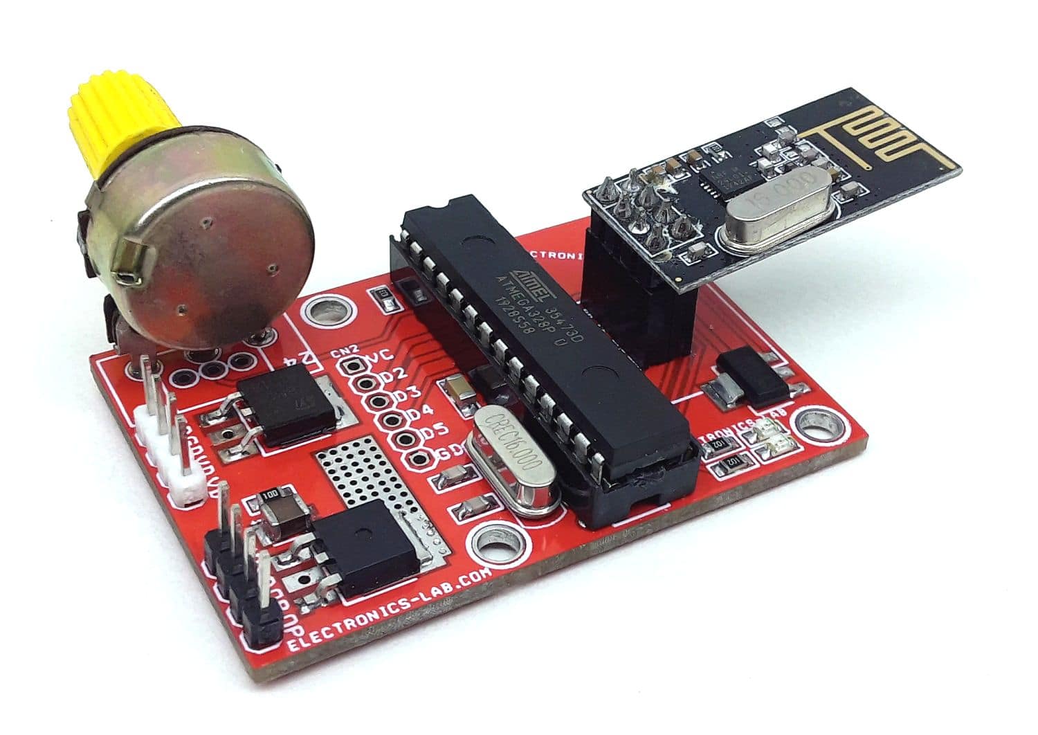
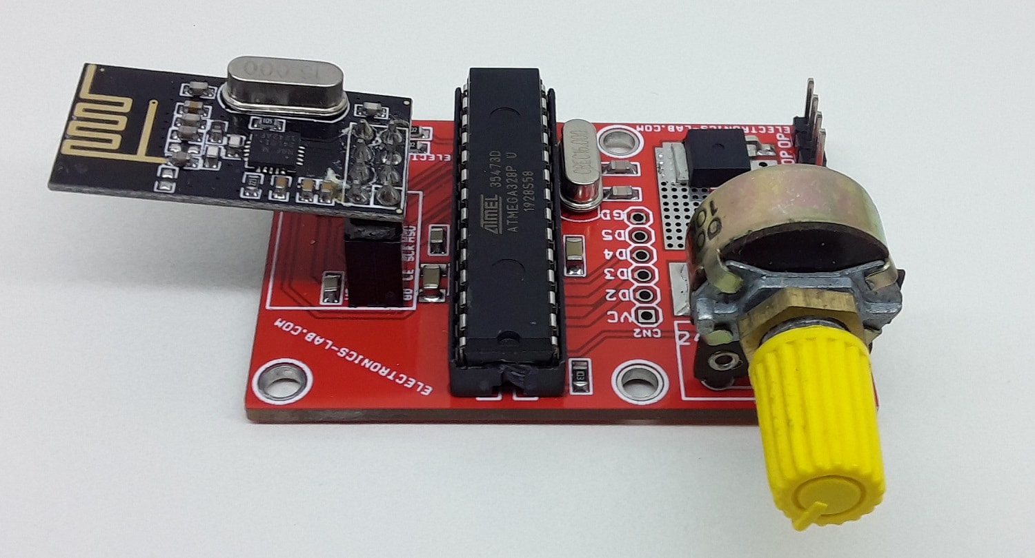
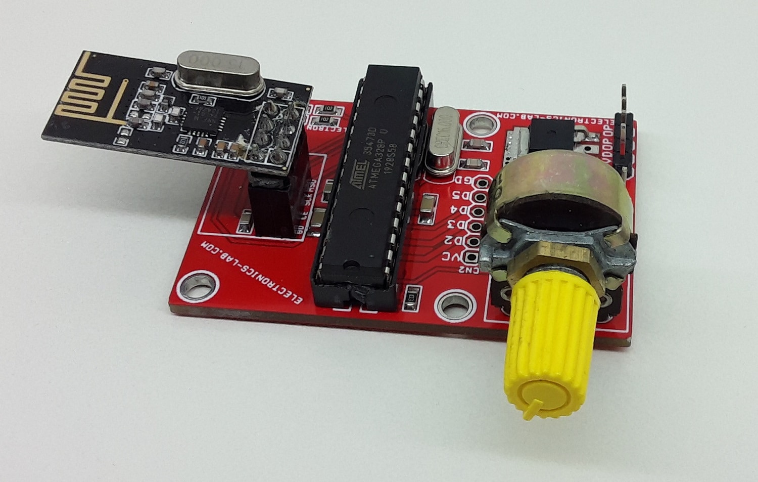
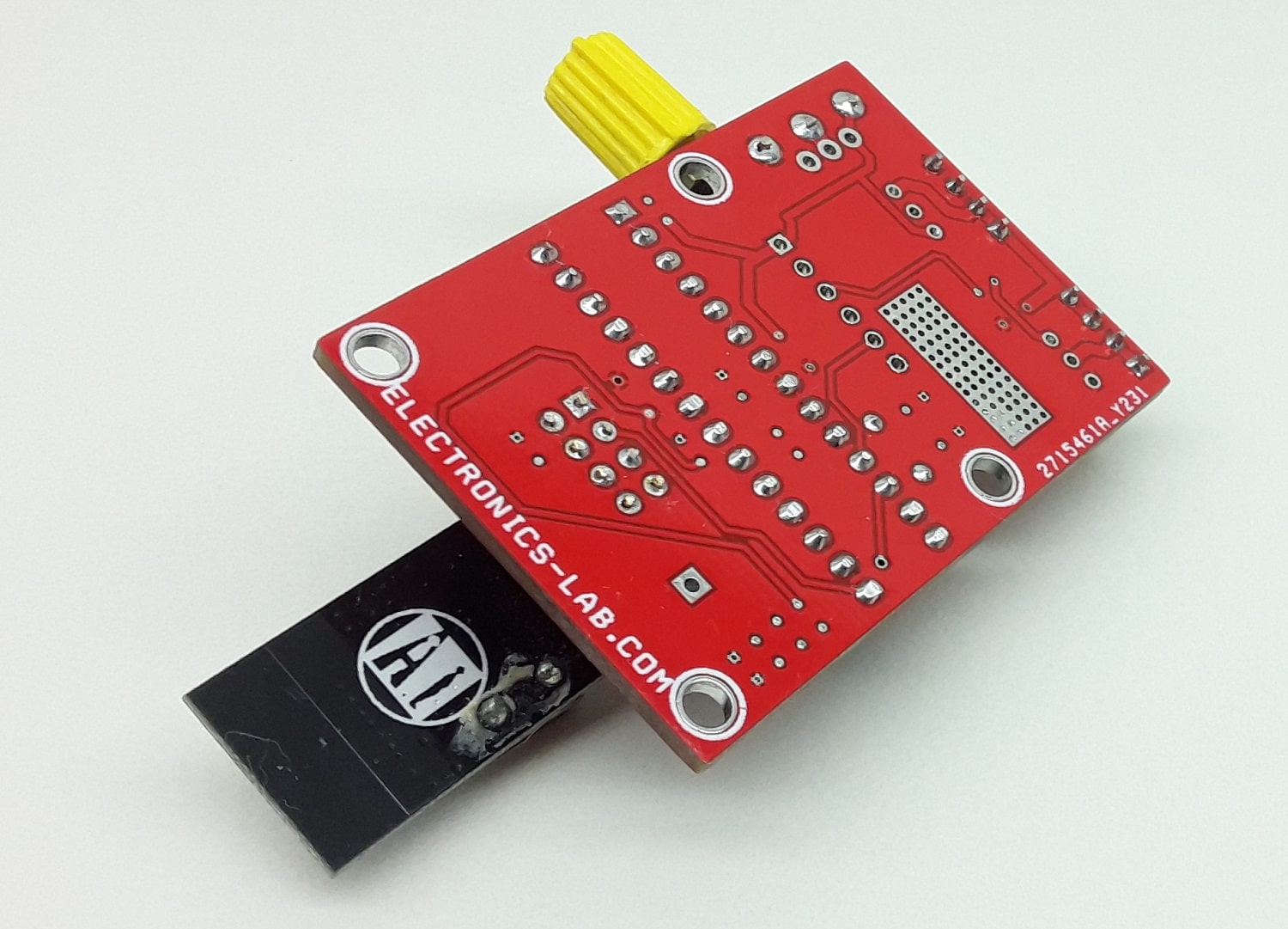
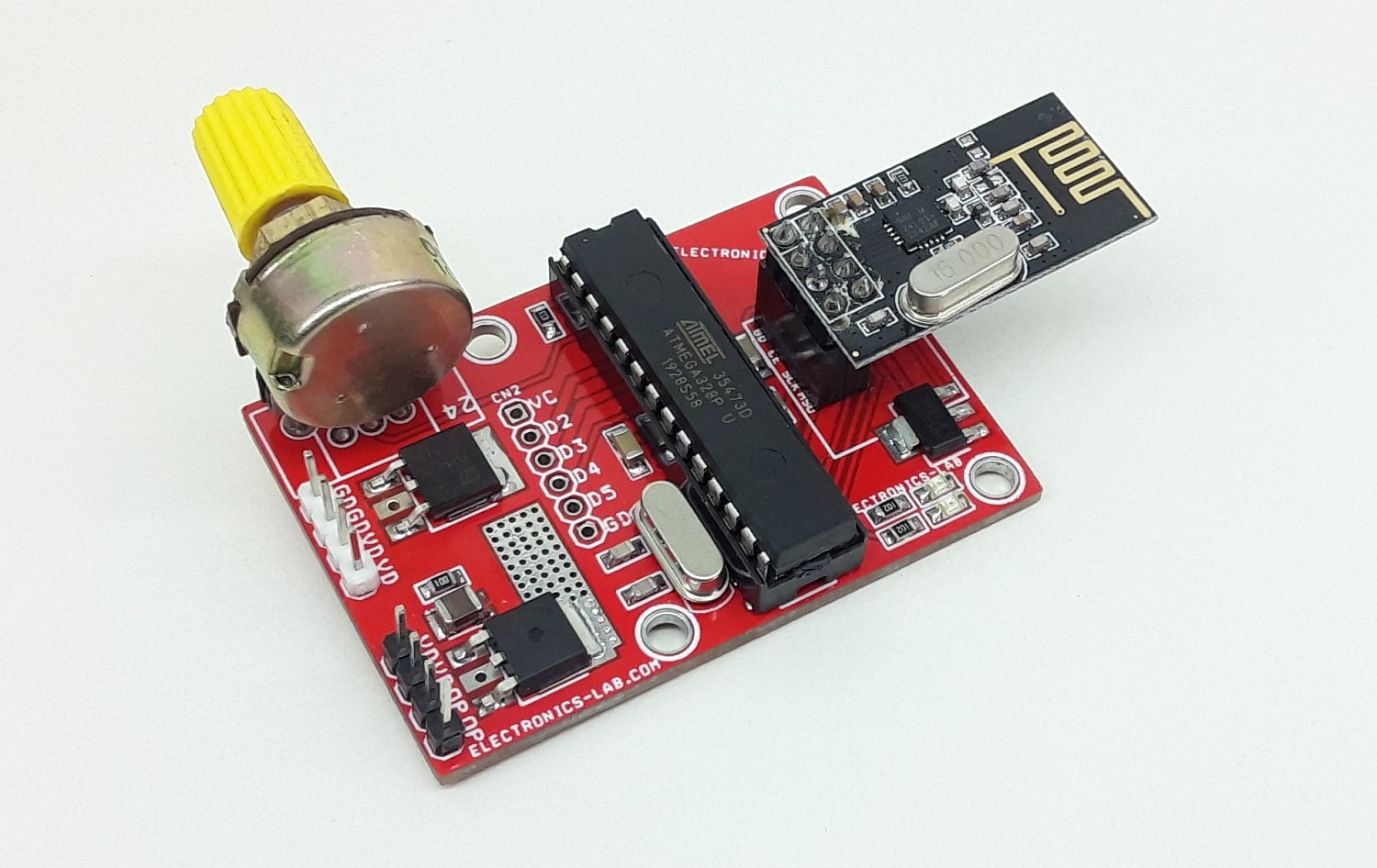
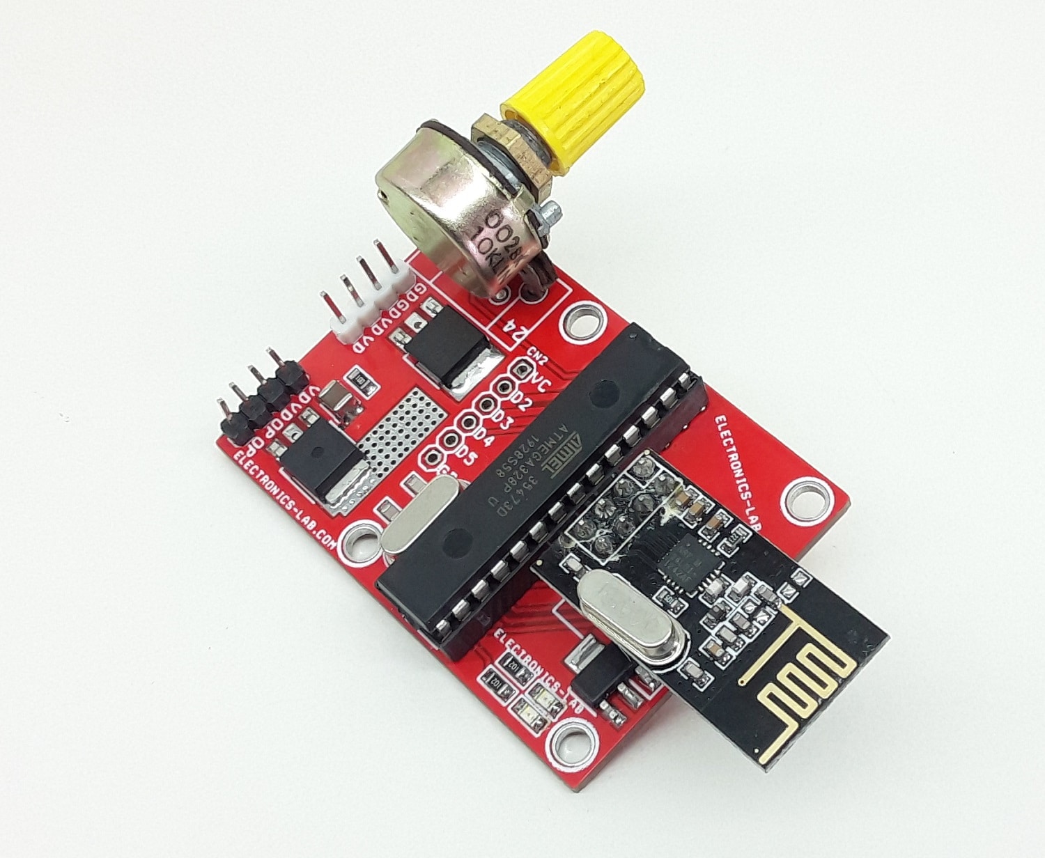
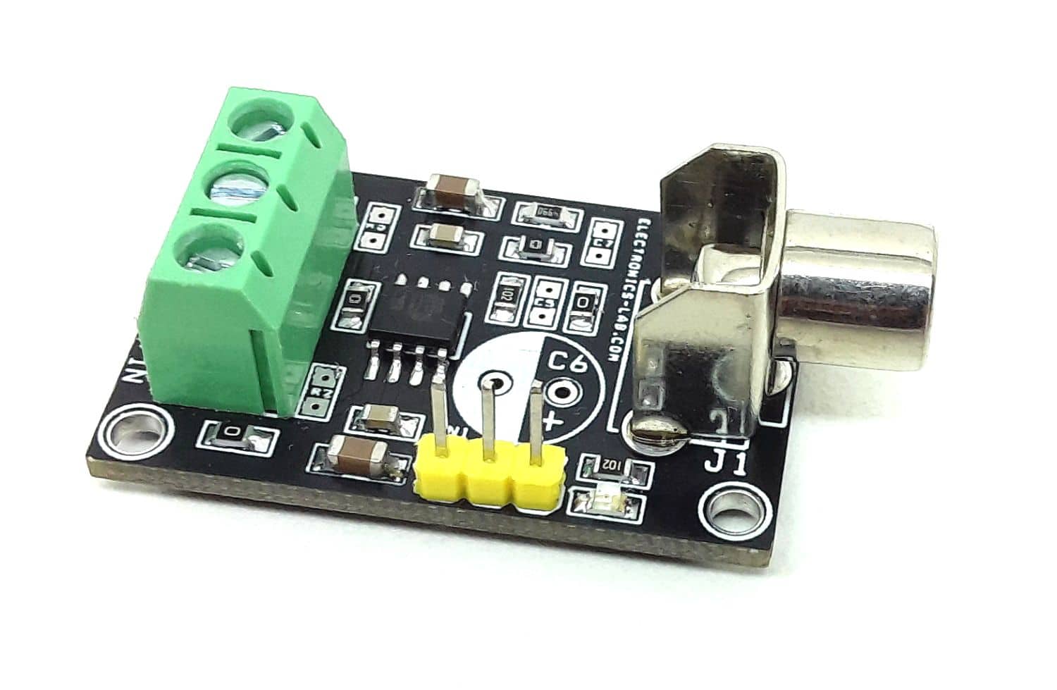
This is an easy-to-make LED dimmer using RF remote control. The project is capable of driving a load up to 24W (2A X 12V LED). Any 12V single or 12V LED strip can be used. This is an open-source Arduino compatible hardware that has Atmega328 microcontroller, Potentiometer, MOSFET, 5V Regulator, 3.3V Regulator, NRF24L01 Radio modules, and few other components. The same PCB can be used for Transmitter and Receiver. LED D2 Power LED, LED D1 optional.
Arduino Pins Transmitter
NRF24L01 RF Module: GND>>GND, 3.3V>>3.3V Regulator, CE>> Arduino Digital Pin D9, CSN>> Arduino Digital Pin D10, MOSI>>Arduino Digital Pin D11, MISO>> Arduino Digital Pin D12, CSK>>Arduino Digital Pin D13
Potentiometer: Analog Pin A3
Arduino Pins Receiver
NRF24L01 RF Module: GND>>GND, 3.3V>>3.3V Regulator, CE>> Arduino Digital Pin D9, CSN>> Arduino Digital Pin D10, MOSI>>Arduino Digital Pin D11, MISO>> Arduino Digital Pin D12, CSK>>Arduino Digital Pin D13
LED Driver MOSFET Gate: Digital Pin D3
Note: PCB has dual options, it can be used for transmitter and receiver, for transmitter don’t install Q1 MOSFET and CN4 connector, for receiver don’t install potentiometer. Upload the related Arduino code that is available as a download.
Credits: This is a modified code, original author R Girish
Arduino Code
Arduino code for transmitter and receiver is available as a download, uploading code is easy, follow bellow link for more details:
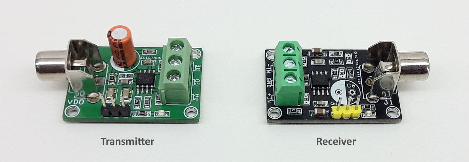
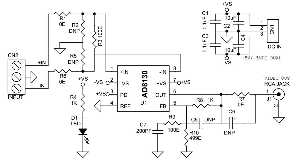
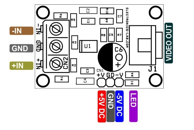
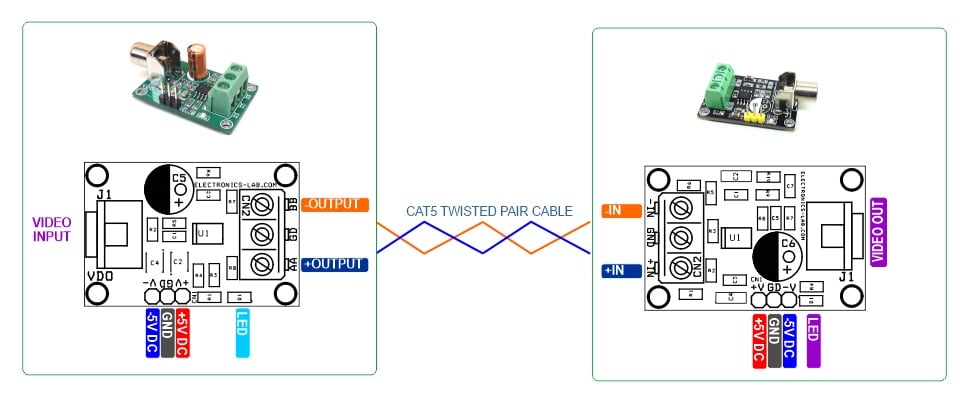
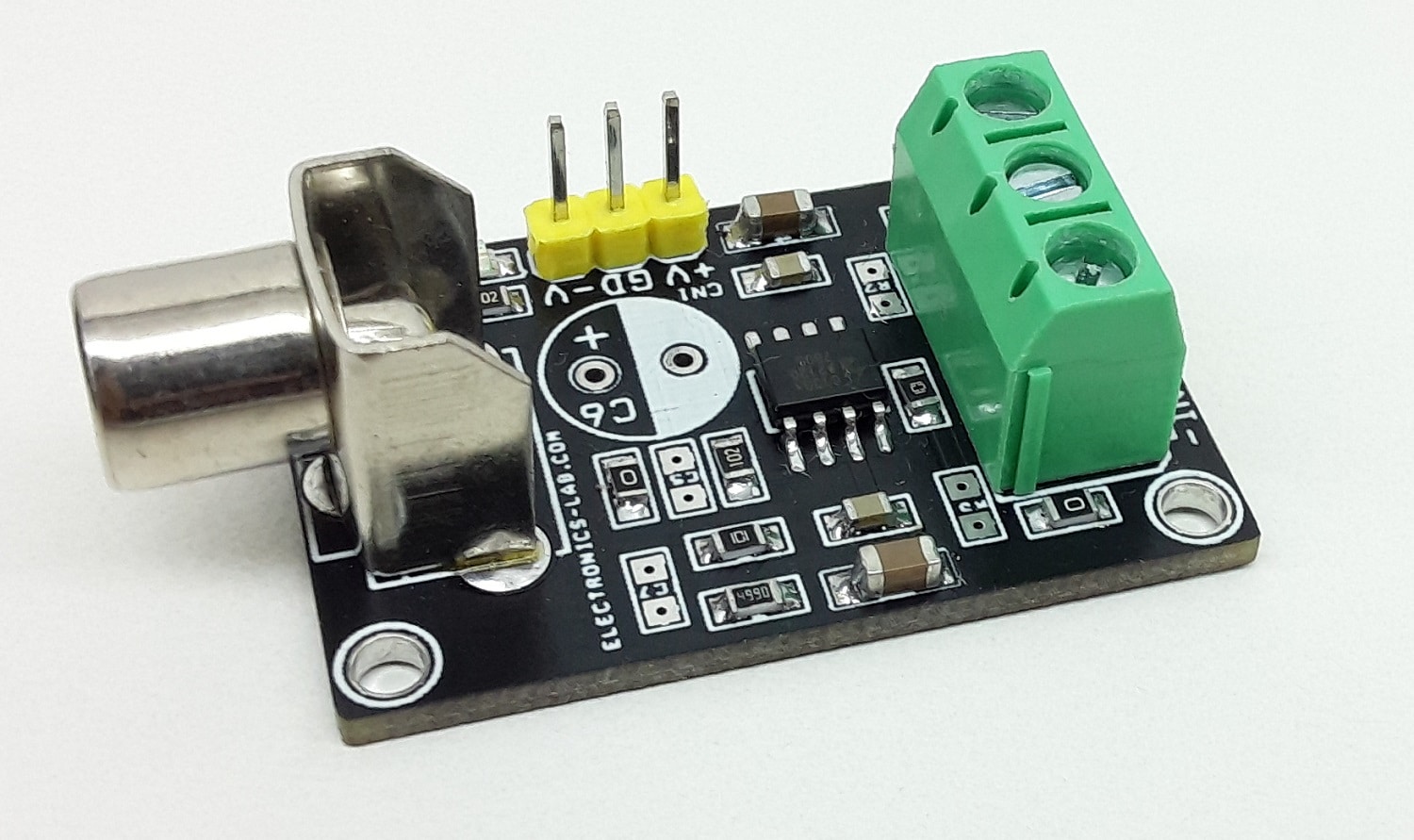
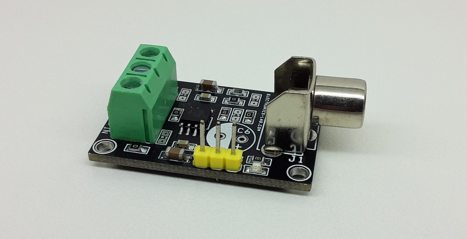
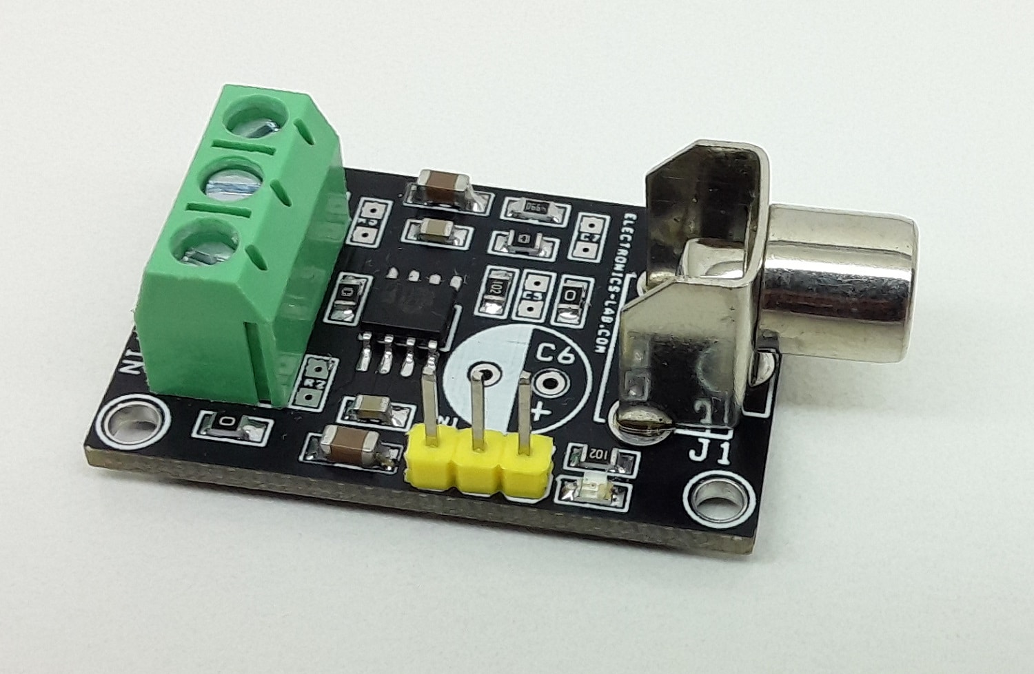
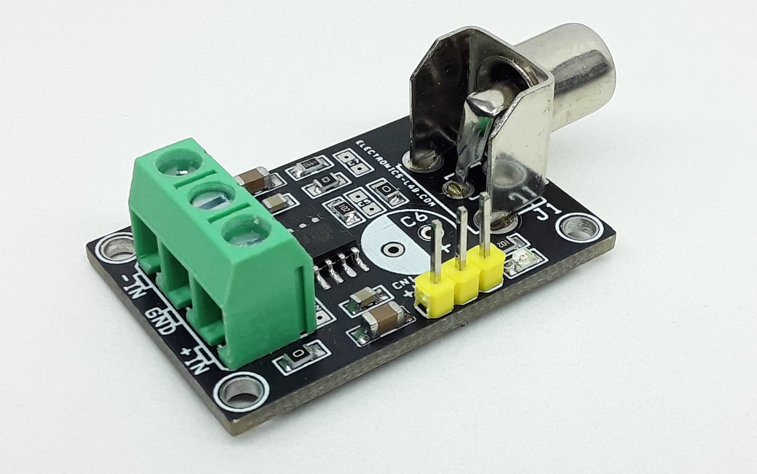
The circuit presented here is a high frequency differential line receiver amplifier which has excellent common-mode rejection at its inputs. The project is an ideal solution for a receiver for composite video signals that are transmitted over long distance on twisted-pair cables like CAT5. Category 5 cables are very common in office settings and are extensively used for data transmission. These cables can also be used for the analog transmission of signals such as video. These long cables pick up noise from the environment they pass through. This noise does not favour one conductor over another and therefore is a common-mode signal. A receiver that rejects the common-mode signal on the cable can greatly enhance the signal-to-noise ratio performance of the link.
Transmitter and receiver work in tandem to convert a Composite Video signal to differential signal and transmit it over a single CAT-5 cable pair to a projector, monitor, or television. Ideal for digital signs, schools, temples, and trade shows. Line driver and line receiver projects can be used to transmit and receive composite video signals over 300 meters of category 5 (CAT-5) cable. The cable has an attenuation of approximately 20dB at 10Mhz for 300 meters.
Features
Operating Supply Dual +5V/-5V (+/-5V) @ 80mA
Compact Solution for Video Transmitter and Receiver over CAT-5 Twisted Cable
Pull-up resistors are used to avoid self-biasing or floating digital inputs. The pull-up resistor connects the digital input to the correct biasing level and eliminates the uncertainty caused by a floating input. A floating input creates a no input condition and may cause random biasing leading to incorrect logic or decision.
A logic gate is a basic building block of a digital circuit and they constitute complex Integrated Circuits (IC’s) and microcontrollers etc. having multiple inputs and outputs connected to external circuitry. These logic inputs and outputs can have only two states that are “0” and “1” or “LOW” and “HIGH”, respectively. These logic states represent two different voltage levels such as a logic “0” by a 0 Volts and logic “1” by a +5 Volts. These logic states are differentiated by different voltage levels or ranges depending upon the type of logic family. Any voltage below a certain level may lead to a “0” state and, on the other hand, any voltage above a certain level may lead to a “1” state.
The digital logic circuits make decisions based on only these two states and a voltage outside of differentiable logic levels could lead to uncertainty and the state of logic “0” or “1” cannot be sensed correctly. Such a condition could falsely trigger a digital circuit or logic gate.
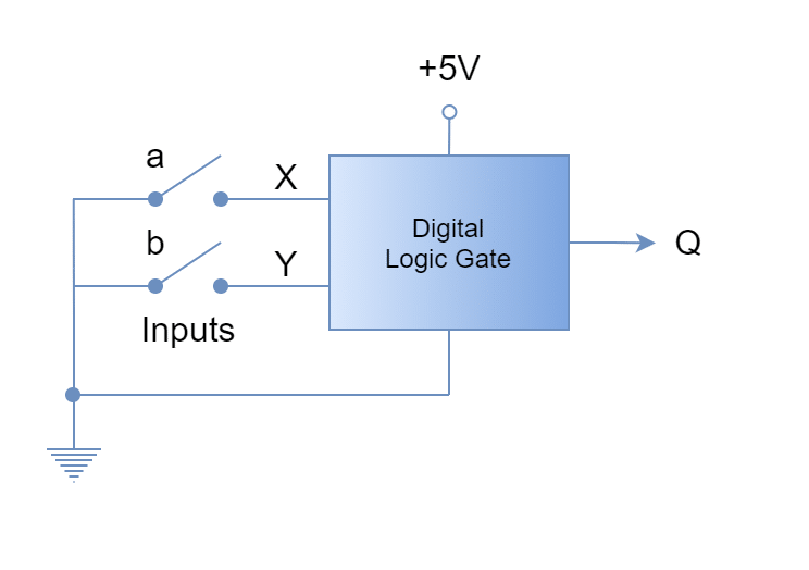
Consider the following digital circuit, the recognizable voltage states for this digital gate are 0V and +5V for logic “LOW” and “HIGH”, respectively. The “X” & “Y” inputs of the digital circuit are connected to the ground (0V) through respective switches namely “a” &”‘b”. When the switch “a” is in close (ON) position then input “X” is connected to ground (0V) which is the correct voltage stage for logic “LOW”. Similarly, the closing of the switch “b” leads to the “LOW” logic state as well.
Figure 1: Inputs to a Digital Gate with open switches
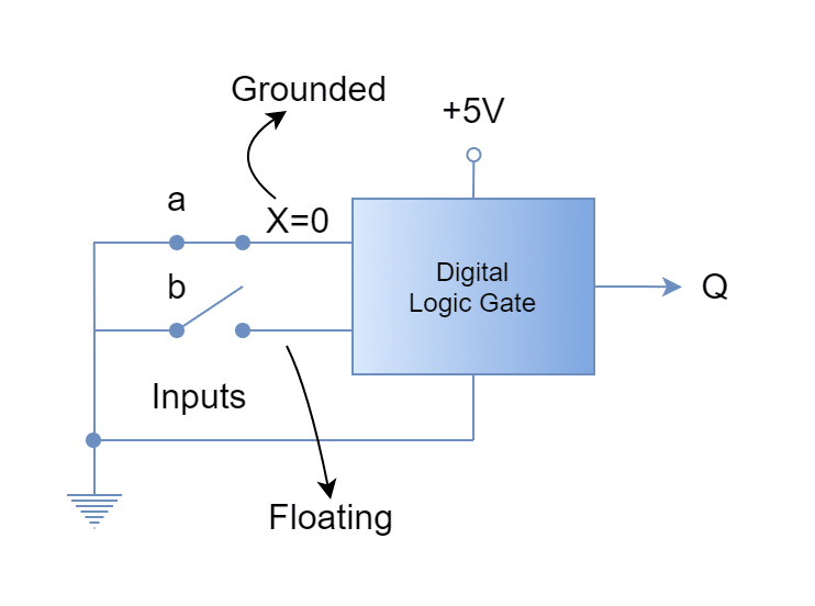
However, when switch ‘a’ is open (OFF) then there is no voltage connected to the input “X” and an expected state would be a logic “HIGH”. But for achieving a logic “HIGH”, the input needs to be connected to +5V which does not seem to be a case here. The input “X” is said to be in the floating condition as it is not effectively connected to any voltage level. Apparently, such a condition may cause input “X” to a have “LOW” logic state but expectations were to have a “HIGH” logic state. Consequently, leading to a false decision at the output “Q”. Moreover, such a floating input is prone to the slightest interferences, and noises could make input change state. The worst could be leading to random shifting of states or oscillation.
Figure 2: Inputs to a Digital Gate with a switch close
The uncertainty, false-triggering, or oscillation in digital circuits due to floating or unused inputs can be prevented by connecting them to a certain voltage level appropriate to the circuit. The tying of inputs defines the logic states in different controlling states of inputs such as seen above in the open switch state where it was unused. In digital circuits, many digital gates or their inputs remain unused and require tying up or down using pull-up or pull-down, respectively. A number of unused inputs prescribing to the same logic state or condition can be tied together using a single pull-up or down resistor.
A pull-up resistor is used to connect an input of the “AND” or “NAND” gate to VCC. Whereas, a pull-down resistor is used to connect the input of the “OR” or ”NOR” gate to the Ground.
Why Pull-up Resistor?
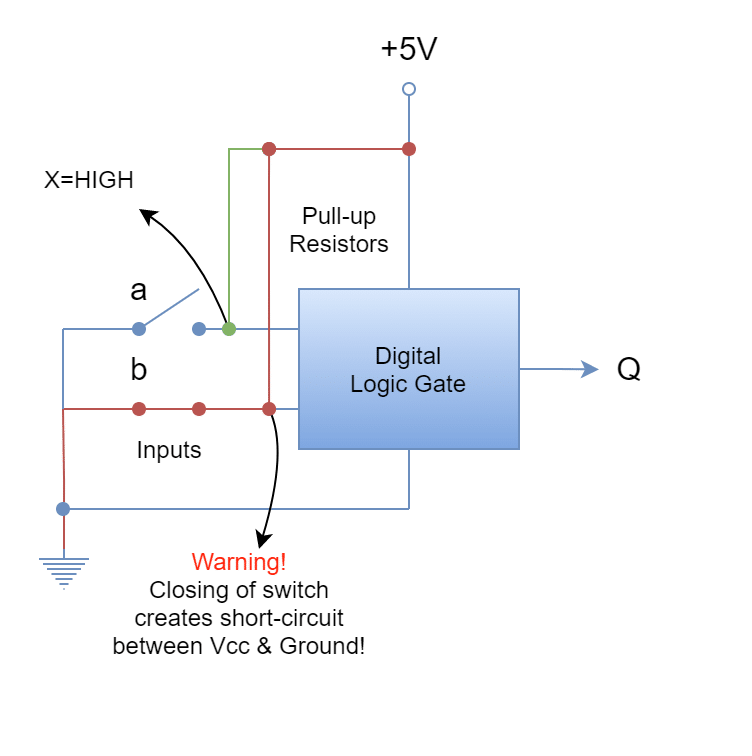
Consider the following diagram of a two-switches case wherein instead of a floating state a second state is achieved by connecting inputs to +5V (a logic “HIGH” voltage level). Now, when switches are open, a logic “HIGH” state is present at the inputs. However, the closing of any switch would short-circuit the +5V with the Ground (0V) and causing an excessive current to flow. This could fry up the digital gate, input, and/ or circuity if there is no short-circuit protection is present. Instead, a pull-up resistor can be used between input and +5V to overcome this issue. The value of the pull-up resistor should be selected in such a way that when pulled-up allows a sufficient voltage drop to bring input voltage to logic “0”.
Figure 3: Inputs to a Digital Gate without pull-up resistors
Pull-up Resistor Application
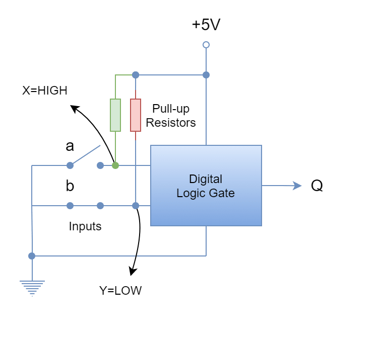
In the following figure, a suitable pull-up resistor is used to pull up each input of the digital circuit. When any of the switches are open (OFF) then the respective input is connected to +5V via this pull-up resistor. The current flowing into the input is very small and, as such, causes a negligible voltage drop across the pull-up resistor. Eventually, a full +5V (nearly) gets applied at the input to bring the logic “HIGH” condition.
Figure 4: Inputs to a Digital Gate with pull-up resistors
Upon closing of any switch, the input is effectively connected to ground (0V) and a firm logic “LOW” condition is sensed by the logic gate/ circuit. However, this time, the VCC and Ground are not shorted due to the insertion of a pull-up resistor and a very little current flow through it. Now, both logic “HIGH” and “LOW” states are effectively achieved in the digital circuit using pull-up resistors. The output (Q) of the digital circuit will reflect the true picture of input states which was initially misleading due to floating inputs.
Calculation of Pull-up Resistor Value
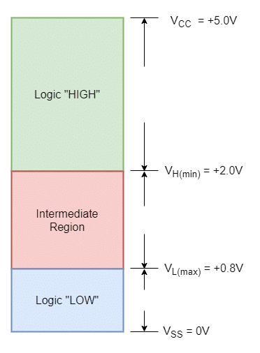
As discussed in previous articles, the logic gates are characterized not only by the operating voltage but also by their current sinking and sourcing capabilities. Besides the two distinct voltage states presenting logic states “0” & “1”, there are maximum and minimum voltages defining voltage ranges for each state. In the following diagram, the voltage ranges for logic “HIGH” and “LOW” states are shown which are separated by an intermediate state.
Figure 5: The logical sensing voltage levels of TTL inputs
It is obvious from the figure that the input needs to have at least 2V to be considered as a logic “HIGH” and, on the other hand, an input should remain below (maximum) a 0.8V to be sensed as a logic “LOW”. In short for a TTL 74LS family, the logic “HIGH” state ranges from 2.0V to 5.0V and the logic “LOW” state from 0.8V to 0V.
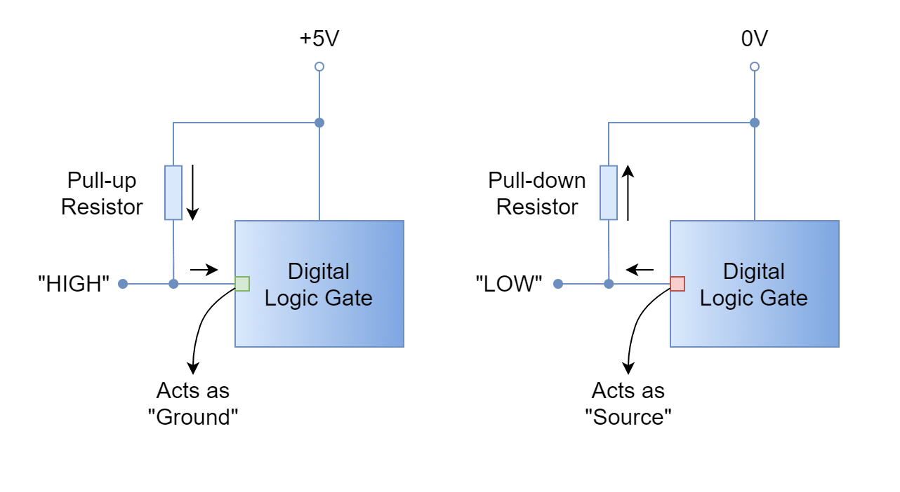
The current flow between input and output of logic gates is dependent on the input logic level i.e. “0” or “1”. The logic “0” level makes the input as current-source as the current flows from input to logic “LOW”. Whereas, a logic “1” makes the input as current-sink and the current now flows towards the input from logic “HIGH”. When an input is at logic “HIGH” then the input acts as a ground and the current flow is considered positive (TTL74LS series have a typical value of 20uA). Likewise, at the logic “LOW” state, the current flows out of the TTL input and is considered negative having a value of -400uA for the TTL74S logic series.
Figure 6: A Digital Input acting as Sink or Source
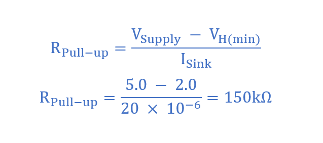
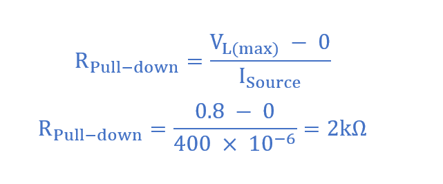
When an input is pulled high it acts as a current sink and positive current flows into it. The TTL74S logic series has a rated positive current of 20uA and a minimum voltage threshold for a logic “1” of 2.0V. In the calculation of the pull-up resistor, the minimum voltage threshold is used to remain on the safest side.
The resistance value obtained above is the maximum value which will ensure a maximum voltage drop of 3V at a minimum 20uA sink current. The voltage is usually kept close to the upper limit of voltage (close to +5V) and this is done by reducing the pull-up resistance value. However, such a close margin can be easily overcome due to resistance tolerance or change in supply voltage, etc. Moreover, the power dissipation is more in low-value pull-up resistance due to an increase in current which should be avoided in any case. The suitable resistance value for a pull-up resistance ranges from 10kΩ to 100kΩ.
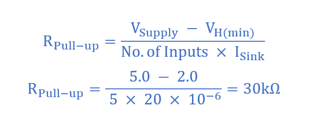
In a similar way, a number of inputs can be tied together using a single pull-up resistance rather than using pull-up resistance at each input, separately. In such a case, the current flowing through single pull-up resistance will number of inputs times the minimum positive (sink) current. In the following calculation, a pull-up resistance value is determined through which five inputs will be pulled up.
Pull-down Resistors
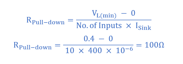
Just like a pull-up resistor, the pull-down resistor ties the input with an effective voltage level. However, contrary to a pull-up resistor, a pull-down resistor connects the input of a logic gate with the Ground (0V) or logic “0” state. The input becomes a current source and supplies current through a pull-down resistor towards the ground. The resistive value of a pull-down resistor for a TTL logic gate is more critical compared to the one used with a similar CMOS gate. It is because of TTL’s high current sourcing capability when its input is in a “LOW” state. The value of the pull-down resistor can be calculated in a similar fashion described above for a pull-up resistor. The TTL 74LS logic series requires a maximum of 0.8V in order to sense it as logic “0” and can deliver a minimum source current of 400uA. The pull-down resistor can be calculated using these parameters as follow:
This is the maximum pull-down resistor which ensures that voltage drop would be sufficient enough at the input to be sensed as logic “LOW”. Further increase in the pull-down resistor value will increase the voltage drop across the resistor and a voltage above 0.8V would be sensed as a logic “HIGH”. The good practice is to keep at least a 0.4V drop across the pull-down resistor.
A number of unused inputs can be connected together with a single pull-down resistor. A sample calculation for a fan-in of 10 is shown below:
The input can be pulled down without using a resistor but is often avoided to avoid excessive current flow or power loss. The pull-down resistor limits the source current flowing towards the ground.
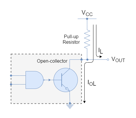
Open-collector Outputs
The outputs of the logic gates are connected with other logic gates which may belong to the same or different logic family. If the output is connected to the same logic family such as TTL to TTL or CMOS to CMOS etc. then logic voltage levels match to produce a coherent result. However, when a connection between two different logic families is required or a load is to be connected to a different voltage level then a logic gate with open-collector output is used. The logic gates are manufactured with the open-collector circuitry at the output of the logic gate. The open-collector output is then derived from desired voltage level using a pull-up resistor. In contrary to the aforementioned pull-up or pull-down which were connected to the logic gate’s input, this pull-up is connected to the output of a logic gate. The term open-collector is used for TTL devices whereas open-drain for CMOS devices.
The open-collector or open-drain outputs are mostly used in inverters, drivers, or buffers where the output is connected to a different voltage level or to deliver high output current which may not be possible using normal logic outputs. For example, driving high current LEDs, relays, DC and servo motors, etc.
In the following figure, the open-collector output of a TTL 74LS01 is shown. In the absence of a pull-up resistor, it is eminent that the output of the logic gate will be either be connected to the ground when “HIGH” or floating when “LOW”. In order to avoid a floating condition, it is necessary to use a pull-up resistor at the output of an open-collector output. The pull-up resistor pulls the output to “HIGH” when the transistor is “OFF” and, upon switching to “ON”, the output becomes “LOW”.
Figure 7: TTL 74LS01 open-collector NAND Gate
Calculation of Open-Collector Pull-up Resistor Value
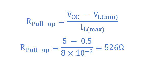
The value of the open-collector pull-up resistor depends upon the load which is driven through it and the current-sinking capability of the open-collector (transistor). When the transistor is in an “ON” state then current flows through the transistor and the value of the pull-up resistor must not exceed the current handling rating of the transistor. On the other hand, the load is supplied through this pull-up resistor when the transistor is in the “OFF” state. In this state, the pull-up resistor value should allow the required load current.
The output voltage levels are required to remain under permissible limits in order to be recognized as logic “LOW” or “HIGH”. For TTL 74LS logic family devices, the minimum “HIGH” logic voltage is 2.7V and the maximum “LOW” logic voltage is 0.5V. In short, the outputs of TTL 74LS devices are considered as logic “LOW” within 0 to 0.5 Volts and as logic “HIGH” within 2.7 to 5.0 Volts.
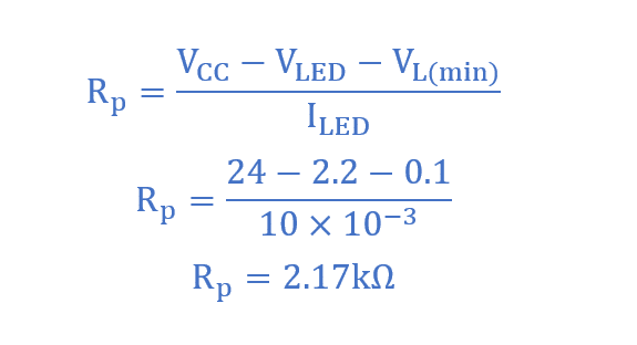
Consider the following calculation as an example for TTL NAND open-collector (74LS01):
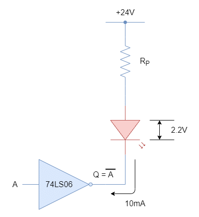
This is the minimum resistance required to limit the current to 8mA which is the maximum current at the logic “LOW” state. In a similar way, the pull-up resistor value can be calculated through which an external load is connected. The external load usually requires high voltage or current and, for this purpose, normally hex inverter buffers are used. The TTL 74LS06 Hex Inverter Buffer uses 5V for biasing but its open-collector can support up to 30 Volts and a maximum of 40mA current at logic “LOW” level.
In the following example, a LED is driven from a 24 Volt supply using a 74LS06 Hex Inverter Buffer. The LED requires 10mA current at a 2.2V voltage drop. The 74LS06 Hex Buffer requires at least 0.1V at the input to sense the “LOW” state. The current limiting resistor value:
Figure 8: Driving a LED from 24V using open-collector output
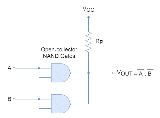
Wired AND Logic
The open-collector outputs can be connected together through a single pull-up resistor. These open-collector outputs tied together forms the Wired AND logic because the outputs are AND’ed together just like they were connected to an AND gate.
Figure 9: Wired AND Gate example
Conclusion
The open-circuits/ floating inputs of digital logic gates may get self-bias leading to false triggering, random switching, or oscillation about logic states.
The pull-up or pull-down resistance is used to tie up a floating input to an effective logic level voltage.
The pull-up resistance ties up the inputs of AND and NAND gates with logic “HIGH” voltage.
The pull-down resistance ties the inputs of OR and NOR gates with the logic “LOW” voltage.
The logic states of “HIGH” and “LOW” levels are distinguished by two different voltage levels. For example, the TTL 74LS series used Ground (0) voltage as logic “LOW” and +5V as logic “HIGH” level.
Besides two distinctive voltages states, there are ranges of voltages that contribute to deciding logic levels. Like, TTL 74LHS Series, has a range from 0 to 0.8V for logic “LOW” and from 2.8 to 5.0V for logic “HIGH”.
The pull-up or down resistance value depends on the logic state of the input. At logic “LOW”, the input becomes a source (positive current) and a sink (negative current), otherwise (logic “HIGH).
The value of pull-down resistance is more critical compared to pull-up resistance because of low input voltage and high current.
The pull-up resistance usually ranges from 1kΩ to 100kΩ and mostly 10kΩ resistance is used in digital circuits. Whereas, the pull-down resistance ranges from 50Ω to 1kΩ.
The pull-up resistances are also used in conjunction with open open-collector (TTL) or open-drain (CMOS) outputs to drive outputs to desired logic voltage.
The open-collector or open-drain outputs are also used for loads requiring high currents such as relays, DC motors or LEDs, etc.
Multiple open-collector outputs connected together through an external pull-up resistance forms a Wired AND Logic.
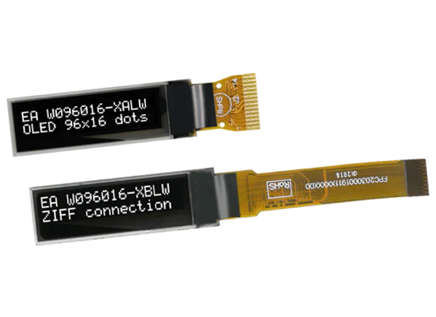
ELECTRONIC ASSEMBLY W09616 0.84” Micro OLED Displays are 96 x 16 dot matrix displays with a 0.22mm pixel pitch that consume low power of 15mA. These OLED displays are capable of offering bright white content with unlimited viewing angles. The W09616 micro OLED displays come included with an SSD1306B controller and feature a 10µs fast response time even at -40°C extreme temperature. These 0.84” OLED graphic displays are ideally suitable for handheld applications.
The EA W096016-XALW incorporates an I²C bus interface and a 10.5mm FPC cable for direct spot welding to the circuit board. The EA W096016-XBLW is equipped with both an I²C bus and an SPI interface. This can be plugged into a 0.3mm ZIFF connector using a 34mm FPC cable with no welding.
Features
0.84” low-power OLED (15mA typical) displays
96×16 dots matrix displays
Bright white content with unlimited viewing angles
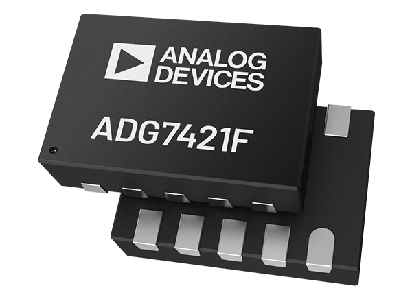
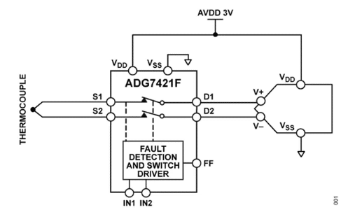
Analog Devices Inc. ADG7421F Dual Single-Pole/Single-Throw Switch features overvoltage protection, power-off protection, and overvoltage detection on the source pins. When no power supplies are present, the switch remains in the off condition, and the switch inputs are high impedance. When powered, if the analog input signal levels on the Sx pins exceed VDD or VSS by a threshold voltage, VT, the switch automatically turns off and the digital FF (fault flag) pin drops to a logic low to indicate a fault.
Features
Overvoltage fault protection up to ±60V on S1 and S2 pins
There’s more to AI than supercomputers and the big things that we often think about when AI is mentioned. Sometimes it is more about bringing AI technology to everyday objects around us and helping people augment what they have in their homes. This is why several companies now look for new ways life can be made easier and better through AI.
UDOO, an embedded computing specialist, is set to launch a crowdfunding campaign for a miniature flexible AI development board named UDOO Key. This microcontroller board combines a Raspberry Pi RP2040, an Espressif ESP32, and AI technology — launching for just $4 (for early backers).
“UDOO KEY is a fully programmable board combining Raspberry Pi RP2040 and ESP32 into a single powerful solution. It allows you to use either RP2040, ESP32 or both to build any AI projects on your terms,” the company writes.
The RP2040 microcontroller has a dual-core Arm Cortex-M0 processor clocked at 133MHz, 264kB of static RAM (SRAM), 8MB of QSPI external flash (4x the amount of the Raspberry Pi Pico) and 8x programmable input/output (PIO) state machines. The ESP32 on the other hand is powered by a dual-core Xtensa 32-bit LX6, 16MB flash memory and 8MB of pseudo-static RAM (PSRAM), and Wi-Fi & Bluetooth connectivity.
The RP2040 is located at the center while the ESP32 is located at the top of the board. You can either use them independently or separately depending on your needs, but the real power of the board lies in using the duo together. Both are fully programmable and compatible with Raspberry Pi Pico accessories and Olimex UEXT accessories.
Other features of the board include a USB Type-C port for data and power along with an expansion header that is based on the Olimex UEXT standard and the ESP32 microcontroller. The board also has an onboard microphone and a nine-axis IMU (inertial measurement unit).
The board is also said to be AI-capable, supporting different programming environments like tinyML and TensorFlow Lite, MicroPython, Arduino IDE and C/C++. The device is also said to support Clea — the AI platform for deploying AI models and applications over a fleet of IoT devices through over-the-air updates.
The board will cost $20 at retail price but early bird backers will have it at a whopping 80% discount which places it at just $4. This “once-in-a-lifetime” price will place the board at the same price level as a Raspberry Pi Pico.
No details yet on when the board will be launched, but you can sign up at the company’s website to get updates and also get notified when the project finally goes live.