Setting up an electronics lab is the dream of many electronics engineers and hobbyists, but getting it done is usually a very big task to achieve. From knowing the amount of space you’d need, to know the right kind of tools to buy, and then to the right kind of devices with the right features and functionalities, you’d agree with me that one needs to be very strategic in the kind of decisions he makes, especially when it comes to choosing from millions of components that are in the market. While we are considering making this a series, providing a series of guides to help with home lab setups, this particular article will focus on some of the components you should have in a Home Lab.
The rule of thumb is to usually stock up with versatile components that could fit into multiple projects and scenarios. This is why we’ve decided to give you some top 20 components that are great to have in an electronics lab.
1. TL431 – a high precision adjustable shunt voltage regulator IC with three poles.
TL431 is capable of regulating voltage from 2.5 to 36V and also delivering 100 mA max output current when configured with an external voltage divider. It is also useful in very low dropout linear regulation when connected with power MOS transistors.
Features and Specifications:
- Voltage Output: 2.5V to 36V
- Current Output: 1mA to 100mA (sink current)
- Tolerance (Output voltage): ±4%
- Output Impedance: 0.22 ohms
- Available in To-92(3-pin) package
- Available in PDIP,SOIC (8-pin) Package
Applications:
- Used in switch-mode power supplies
- Used in linear regulation
- Used as voltage comparators
Download the datasheet for more information and configuration.
2. Nios II – a 32-bit configurable soft microprocessor.
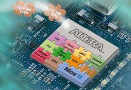
Nios II is a RISC-designed embedded processor with 32 general-purpose registers, specifically built for compatibility with the Altera family of field-programmable gate array (FPGA) integrated circuits. It is an enhanced Nios architecture with many improved functionalities, thus suitable for usage in a wider range of embedded computing applications.
The Nios II finds wide application in a variety of areas including digital signal processing (DSP) and system-control. Its soft-core processor offers flexibility to system designers by allowing customized cores for specific application requirements.
Features and specifications:
- Design: RISC soft-core architecture which is implemented entirely in the programmable logic and memory blocks of Altera FPGAs.
- Opensource: NO
- Bits: 32 general-purpose 32-bit registers, full 32-bit instruction set, data path, and address space, Single-instruction 32 × 32 multiply and divide producing a 32-bit result.
- Expandable Functions: By adding a predefined memory management unit, or defining ustom instructions and custom peripherals
3. LM1117T-3.3 – a low voltage dropout regulator
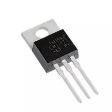
LM1117T-3.3 by Texas Instruments, is a fixed version of LM1117 series with 3.3V output, 80mA output, 15V max input and 1.2V dropout voltage. It is a one output positive linear regulator and can offer current limiting and thermal shutdown. LM1117 family is designed to operate under a wide temperature range.
Features and Specifications:
- Output Voltage: 3.3 V
- Output Current: 800 mA
- Number of Outputs: 1 Output
- Polarity: positive
- Quiescent Current: 10 mA
- Input Voltage MAX: 15 V
- Output Type: Fixed
- Minimum Operating Temperature: 0°C
- Maximum Operating Temperature: +125C
- Dropout Voltage: 1.2 V
- Dropout Voltage – Max: 1.2 V at 100 mA, 1.25 V at 500 mA, 1.3 V at 800 mA
- Voltage Regulation Accuracy: 1 %
- Ib – Input Bias Current: 5 mA
- Line Regulation: 1 mV
- Load Regulation: 1 mV
- Subcategory: PMIC – Power Management ICs
Applications:
- Used as a regulator for switching AC/DC converter
- Used in high-efficiency linear regulations
- Used in battery charger and battery-powered instrumentation
- Used in AC drive power stage modules
- Used in merchant network and server PSU
- Used in ultrasound scanners, servo drive control modules
Download the datasheet for more information and configuration.
4. Blackfin – a family of 16-/32- bit microprocessors manufactured by Analog Devices
Blackfin incorporates a built-in, fixed-point digital signal processor (DSP) functionality supplied by 16-bit multiply-accumulates (MACs) with an on-chip microcontroller. The Blackfin is designed specifically for a unified low-power processor architecture capable of executing OS and complex numeric tasks at the same time. It can also handle real-time H.264 video encoding processes.
Features and Specifications:
- Bits: 32-bits
- Design: RISC
- Register Encoding: Variable (16- or 32-bit general-purpose, or 64-bit parallel issue of 1 × 32-bit instruction + 2 × 16-bit instructions)
- Branching: Condition code
- Registers: General purpose 8 × 32-bit data registers (addressable as 16 × 16-bit half-registers), 2 × 40-bit accumulators, 6 × 32-bit address registers, stack pointer, frame pointer
5. PC817 – an optocoupler designed with a phototransistor and an Infrared emitting diode (IRED/IRD), creating an optical bridge.
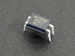
PC817 IC acts as a filter used to provide electrical isolation of a signal between two circuits; eliminating noise from incoming signals. It can be used to provide wired isolation between a microcontroller and high energy load circuit allowing technicians and hobbyists to drive heavy loads with digital inputs/signals. The IC is compatible with a wide range of devices such as TTL devices and High DC loads.
Features and Specifications:
- 4-pins, available in two packages like SMT and DIP
- 5kV internal protection for I/O from electrical isolation
- Used with an additional resistor to drive high voltage devices through fewer voltage devices.
- Forward Voltage of Input Diode: 1.25V
- Collector maximum current ratio: 50mA
- Collector-Emitter Voltage: 80V (max)
- Collector & Emitter maximum voltage ratio: 80V
- Maximum Collector Current: 50mA
- Rise Time is 18us
- Fall Time is 18us
- Cut-off frequency: 80kHz
- Power Dissipation: 200mW.
- The internal resistance: 100 ohms.
- While soldering, the optocoupler’s soldering temperature range: 260 degrees (Maximum)
Applications:
- Used at computer/microcontroller terminals for I/O isolation
- Used in system appliances and measuring instruments
- Used for noise suppression in switching circuits
- Used in registers, copiers and automatic vending machines
- Used in electric home appliances, such as fans, and heaters
- Used in signal transmission between circuits of different potentials and impedances
Download the datasheet for more information and configuration.
6. ATmega328 – a single-chip microcontroller with an enhanced Harvard architecture 8-bit RISC processor core.
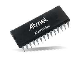
ATmega328 is a member of Atmel’s AVR family. It takes an input voltage of 1.8 to 5.5V, and runs at a maximum clock speed of 20 MHz achieving a throughput near 1 MIPS/MHz. It is furnished with 32 KB ISP flash memory with read-while-write capabilities, 1 KB EEPROM, and 2 KB SRAM.
Features and Specifications:
- Design: Atmel 8-bit AVR RISC-based microcontroller
- Input Voltage: 1.8 – 5.5 V
- Maximum CPU speed: 20 MHz
- Throughput: near 1 MIPS/MHz
- Memory: 32 KB ISP flash memory with read-while-write capabilities, 1 KB EEPROM, 2 KB SRAM.
- Registers: 32 general-purpose working registers, internal and external interrupts
- Pin-out and Peripherals: 23 general-purpose I/O lines, serial programmable USART, a byte-oriented 2-wire serial interface, SPI serial port, 6-channel 10-bit A/D converter (8 channels in TQFP and QFN/MLF packages), programmable watchdog timer with internal oscillator, 3 flexible timer/counters with compare modes and 5 software-selectable power-saving modes.
Applications:
- Commonly used in projects and autonomous systems where a simple, low-powered, low-cost microcontroller is needed.
- Used on Arduino development platform for Arduino Uno and Arduino Nano models.
7. LM317 – an adjustable positive linear voltage regulator, analogous to the 78xx series standard fixed regulators.
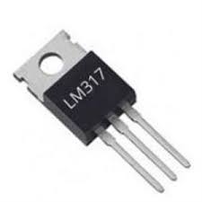
LM317 offers a maximum output current of 32mA at 5V output in a constant voltage mode with 34V input supply. The IC also supplies a maximum current of 117mA in a constant current mode with an input voltage at 12 V and a forward voltage drop of 3.6 V.
Specifications:
- Output voltage range: 1.25 – 37 V
- Voltage differential: 3 – 40 V
- Maximum output current: 1.5 A
- Minimum load current: 3.5 mA typical, 12 mA maximum
Applications:
- Used as a voltage regulator
- Used as current regulator
- Used in DC to DC converter applications
Download the datasheet for more information and configuration.
8. ATtiny85 – low-power CMOS 8-bit microcontroller based on the megaAVR enhanced RISC architecture.
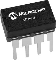
The ATtiny85 is an Atmel Semiconductor’s ATtiny85 that allows system designers to optimize power consumption by executing complex instructions in a single clock cycle to achieve throughputs near 1 MIPS/MHz. It operates from a supply in the range of 2.7 – 5.5V and runs at max. 20 MHz.
Features and Specifications:
- Working Voltage: 2.7 – 5.5 V
- Max. Operating Frequency: 20 MHz
- CPU: 8-bit AVR
- Flash: 8 Kbytes
- Pin Count: 8
- Max I/O Pins: 6
- Hardware QTouch Acquisition: No
- Ext Interrupts: 6
- USB Interface: No
- USB Speed: No
- Peripherals: Brown-out Detect / Reset / POR / PWM / Watchdog
- Portable and lightweight design, and easy to use.
- High quality, wear-resistant and durable.
9. ICM7555 – a general-purpose timer IC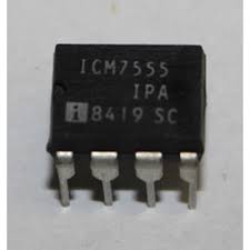
ICM7555 is a CMOS RC timer that provides enhanced functionality than the 55/6 and 355 timers and is a replacement for those devices in most applications today. It has improved parameters such as wide operating supply voltage range, low supply current, trigger and reset currents, low threshold, and higher frequency performance. In addition, it has no crowbarring of the supply current during output transitions and no requirement to decouple control voltage for stable operation. Specifically, the ICM7555 is designed for a stable controller capable of producing accurate time delays or frequencies in applications.
Features and Specifications:
- Low Supply Current: 60μA
- Extremely Low Input Currents: 20pA
- High-Speed Operation: 1MHz
- Guaranteed Supply Voltage Range: 2V to 18V
- Normal Reset Function – No Crowbarring of Supply During Output Transition
- Can be Used with Higher Impedance Timing Elements than Regular 555/6 for Longer RC Time Constants
- Timing from Microseconds through Hours
- Operates in Both Astable and Monostable Modes
- Adjustable Duty Cycle
- High Output Source/Sink Driver can Drive TTL/CMOS
- Outputs have Very Low Offsets, HI and LO
- Pb-Free Plus Anneal Available (RoHS Compliant)
Applications:
- Used precision timing
- Used in pulse generation
- Used in sequential timing
- Used in time delay generation
- Used in pulse width modulation
- Used in pulse position modulation
- Used in missing pulse detection
Download the datasheet for more information and configuration.
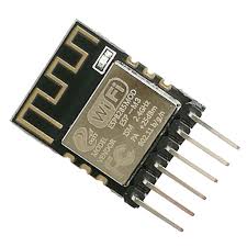
10. ESP32 – a series of low-cost, low-power system-on-chip microcontrollers with integrated Wi-Fi and dual-mode Bluetooth
ESP32 is a successor to EspressIf System industry’s standard ESP8266. Specifically, the ESP32 depending on it’s version, utilizes either a Tensilica Xtensa LX6 microprocessor in both dual-core and single-core variations, Xtensa LX7 dual-core microprocessor, or a single-core RISC-V microprocessor. It has an operating speed of 160/240 MHz and uses as low as 5uA at deep sleep mode.
Features and Specifications:
-
- CPU: Xtensa dual-core (or single-core) 32-bit LX6 microprocessor, operating at 160 or 240 MHz and performing at up to 600 DMIPS
- Ultra-low-power (ULP) co-processor
- Memory: 320 KiB RAM, 448 KiB ROM
-
- Wi-Fi: 802.11 b/g/n
- Bluetooth: v4.2 BR/EDR and BLE (shares the radio with Wi-Fi)
-
- 34 × programmable GPIOs
- 12-bit SAR ADC up to 18 channels
- 2 × 8-bit DACs
- 10 × touch sensors (capacitive sensing GPIOs)
- 4 × SPI
- 2 × I²S interfaces
- 2 × I²C interfaces
- 3 × UART
- SD/SDIO/CE-ATA/MMC/eMMC host controller
- 1 x SDIO/SPI slave controller
- Ethernet MAC interface with dedicated DMA and IEEE 1588 Precision Time Protocol support
- 1 x CAN bus 2.0
- Infrared remote controller (TX/RX, up to 8 channels)
- Motor PWM
- LED PWM (up to 16 channels)
- 1 x Hall effect sensor
- 1 x Ultra low power analog pre-amplifier
-
- IEEE 802.11 standard security features all supported, including WPA, WPA2, WPA3 (depending on version) and WAPI
- Secure boot
- Flash encryption
- 1024-bit OTP, up to 768-bit for customers
- Cryptographic hardware acceleration:
- AES, SHA-2, RSA, elliptic curve cryptography (ECC), random number generator (RNG)
-
- Internal low-dropout regulator
- Individual power domain for RTC
- 5 μA deep sleep current
- Wake up from GPIO interrupt, timer, ADC measurements, capacitive touch sensor interrupt
Applications:
- Used in commercial devices such as IoT LED wristband, biometric attendance-tracking system, remotely controllable, LED-based light, and aromatherapy devices to mention a few.
- Used in industrial devices for industrial automation and monitoring, supporting digital inputs/outputs, analog inputs, and various computer networking interfaces.
Download the datasheet for more information configuration.
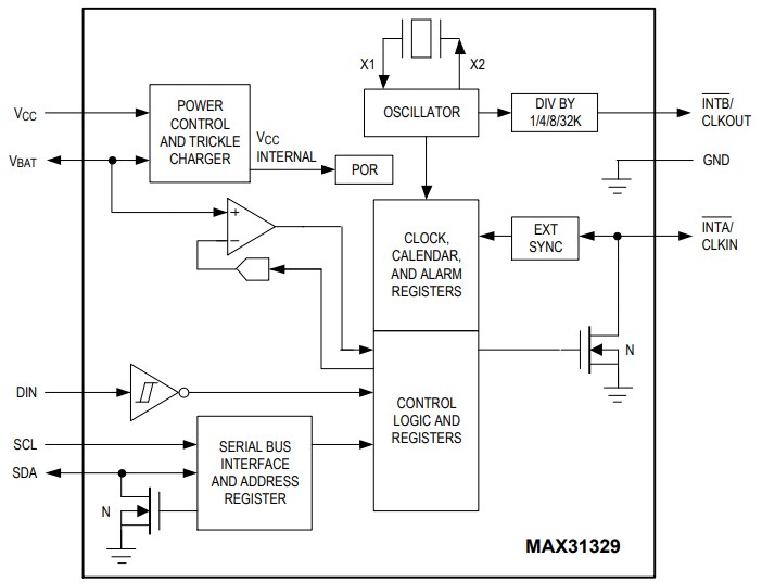
11. PCF8523 – low powered CMOS Real-Time Clock (RTC) and calendar
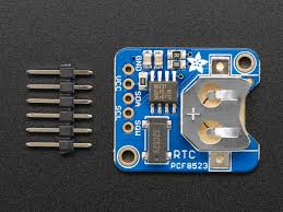
PCF8523 features an I²C-bus for serial data transfer at 1000 kbit/s maximum throughput. In addition, it has an offset register for clock-tuning, alarm and timer functions to generate wake-up signals at the trigger, and a backup battery switch-over circuit for automatic changeover to battery when there is a power failure.
Features and Specifications:
- Provides year, month, day, weekday, hours, minutes, and seconds based on a 32.768 kHz quartz crystal
- Resolution: seconds to years
- Clock operating voltage: 1.0 V to 5.5 V
- Low backup current: typical 150 nA at VDD = 3.0 V
- Battery backup input pin and switch-over circuit
- Freely programmable timer and alarm with interrupt capability
- Selectable integrated oscillator load capacitors for CL = 7 pF or CL = 12.5 pF
- Internal Power-On Reset (POR)
- Open-drain interrupt or clock output pins
- Programmable offset register for frequency adjustment
Applications:
- Used in time-keeping application
- Used in battery-powered devices
- Used in metering for accuracy, precision, and detailing.
Download the datasheet for more information configuration.
12. nRF52832 – the latest multiprotocol radio System on Chip (SoC) designed and manufactured by Nordic Semiconductor
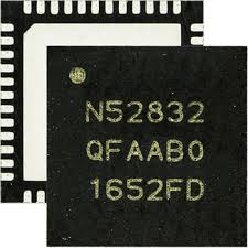
nRF52832 features an ARM Cortex-M4F MCU with a 2.4GHz radio transceiver and can operate on a power supply of 1.7 to 3.6V range. It also consists of a 3.3V regulator with a maximum input of 6V for battery-powered or regulated supply applications.
Features and Specifications:
- Working Voltage: 1.7 – 3.6V
- Communication: proprietary 2.4GHz multiprotocol radio
- CPU: 32-bit ARM Cortex-M4F Processor
- Memory: 512kB flash, and 64kB RAM.
- Peripherals: 32 configurable I/O pins, SPI, I2C, UART, PWM, ADC’s, Bluetooth Low Energy (BLE), and 32.768kHz RTC Crystal
13. MCP6042 – dual operational amplifier with a gain-bandwidth product of 14 kHz and low normal operating current of 600 nA
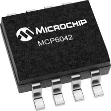
MCP6042 has an offset voltage of less than 3 mV, takes a minimum input voltage of 1.4V, and utilizes a quiescent current less than 2.0 uA by both amplifiers. The IC offers enhanced features such as high open-loop gain, rail-to-rail output swing, high-speed operation, and low current bias as a result of utilizing advanced CMOS technology.
Features and Specifications:
- Low Quiescent Current: 600 nA/amplifier (typical)
- Rail-to-Rail Input/Output
- Gain Bandwidth Product: 14 kHz (typical)
- Wide Supply Voltage Range: 1.4V to 6.0V
- Unity Gain Stable
- Available in Single, Dual, and Quad
- Chip Select (CS) with MCP6043
- Available in SOIC and MSOP packages
- It has been tested and qualified in accordance with AEC-Q100 requirements.
Applications:
- Ideal for industrial process control
- Low-power battery-operated devices Portable equipment and wearable products.
- For automotive design and applications.
Download the datasheet for more information configuration.
14. ESP32-C3 – a modified Espressif’s ESP32, a cost-effective, RISC-V-based MCU with Wi-Fi and Bluetooth 5 (LE) connectivity
ESP32-C3 is a single-core, 32-bit microcontroller with 400KB SRAM and a clock speed of 160MHz. Its integrated Wi-Fi is rated 2.4 GHz while its Bluetooth 5 (LE) can operate at long-range. ESP32-C3 seeks to meet the most common needs for connected devices by providing a simple and secure connectivity for IoT applications.
Features and Specifications:
- Design: single-core, 32-bit, RISC-V-based
- Processing Speed: 160MHz
- Memory: 400KB of SRAM
- Connectivity: 2.4 GHz Wi-Fi and Bluetooth 5 (LE) with a long-range support
- Peripherals: 22 programmable GPIOs with support for ADC, SPI, UART, I2C, I2S, RMT, TWAI, and PWM.
Download the datasheet for more information configuration.
15. LM393 – a voltage comparator operational amplifier with an open collector output
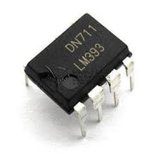
LM393 IC consists of two high precision autonomous voltage comparators that can be operated with either a single or split supply range of 2 to 36V or of +/- 1 to 18V respectively.
Features and Specifications:
- Low input offset voltage: 5.0 mV
- Low operating current: 0.4 mA
- Operates from a single positive power supply: 2 to 36V
- Operate from a split supply: ± 1.0 to ±18V
Applications:
- Voltage comparator
- To monitor an analog signal to see if it goes beyond a threshold that requires some action to be taken.
- Used as a relay or LED driver
- Used with a microcontroller for digital monitoring of analog sensors
Download the datasheet for more information configuration.
16. ESP8285 – a Wi-Fi Chip specifically designed for wearable devices
Espressif’s ESP8285 is an improved ESP8266 with a flash memory of 1MB. It finds a widespread application in devices such as smartwatches, smart glasses, activity monitors, and smart bracelets. The chip also incorporates an enhanced version of Tensilica’s L106 Diamond series 32-bit processor and functionalities to meet efficient power usage and reliable performance demands of IoT.
Features and Specifications:
- Supply voltage: 3 – 3.6 V.
- Current consumption: (Continuous transmission => Average: ~ 71mA, Peak: 300mA, Sleep: ~ 20mA)
- Program memory size: 1MB
- UART speed: up to 4 Mbps
- Program memory operating mode: DOUT (in other modes this memory does not work)
- Interface support: UART / GPIO / PWM / ADC
- Built-in lwIP protocol stack
- Supports data transmission modes: STA / AP / STA + AP – Supports Smart Config / AirKiss technology
- Supports Remote Firmware Upgrade (FOTA)
- Module Form Factor: DIP-18
- SPI Flash: Built-in 1MB
- Interface: UART / GPIO / PWM / ADC
- I / O ports: 11
- UART baud rate: 300-4608000 bps, default 115200
- Frequency range: 2412-2484 MHz
- Antenna: built-in, 2dBi
- Working temperature: – 20 – 85 С
- Dimensions: 15×12 mm
Applications:
- Wearable devices
- If your project does not have enough memory or computing resources, but at the same time, ESP32 is redundant.
- IoT applications
Download the datasheet for more information configuration.
17. 74HC4052 (or 74HCT4052) – a dual single-pole 4-channel analog switch
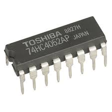
74HC4052 is suitable for use as an analog and digital multiplexing/demultiplexing. Each of its two switches feature four independent inputs/outputs and a common input/output pole. The IC also has a digital enable input and two digital select inputs common to both switches. To turn OFF the switches, the digital enable pin is set ON. 74HC4052 allows clamps diodes as inputs.
Features and Specifications:
- Wide analog input voltage range: -5 V to +5 V
- CMOS low power dissipation
- High noise immunity
- Latch-up performance exceeds 100 mA per JESD 78 Class II Level B
- Low ON resistance:
- 80 Ω (typical) at VCC – VEE = 4.5V
- 70 Ω (typical) at VCC – VEE = 6.0V
- 60 Ω (typical) at VCC – VEE = 9.0V
- Logic level translation: to enable 5 V logic to communicate with ±5 V analog signals
- Input levels:
- For 74HC4052: CMOS level
- For 74HCT4052: TTL level
Applications:
- Analog multiplexing and demultiplexing
- Digital multiplexing and demultiplexing
- Signal gating
Download the datasheet for more information configuration.
18. MSP430G2452 – an MP430 series of ultra-low-power mixed signal microcontroller
MSP430G2452 is furnished with a 16MHz microcontroller unit that has an 8kB Flash and 256B SRAM. It also consists of a 10-bit A/D converter, an analog comparator, timer and SPI/I2C for universal serial communication.
Features and Specifications:
- Low Supply Voltage Range: 1.8 – 3.6V
- Ultra-Low Power Consumption
- Active Mode: 220µA at 1 MHz, 2.2V
- Standby Mode: 0.5 µA
- Off Mode (RAM Retention): 0.1 µA
- 16-Bit RISC architecture, 62.5-ns instruction cycle time
- Ultra-fast wake-up from standby mode in less than 1 µs
- Basic clock module configurations
- Internal frequencies up to 16 MHz
- Internal Very-Low-Power Low-Frequency (LF) Oscillator
- 32-kHz Crystal
- External digital clock source
- One 16-Bit timer_A with three capture/compare registers
- Up to 16 capacitive-touch enabled I/O pins
- Universal Serial Interface (USI) Supporting SPI and I2C
- 10-Bit 200-kbps Analog-to-Digital (A/D) Converter With Internal
- Reference, Sample-and-Hold, and Autoscan (MSP430G2452 Only)
- On-Chip Comparator for Analog
- Brownout Detector
- Serial onboard programming, No external programming voltage
- On-Chip Emulation Logic With Spy-Bi-Wire Interface
Applications:
- Used in low-cost sensor systems that capture analog signals
- Used in A/D Converter systems/circuits
Download the datasheet for more information configuration.
19. 74HC595 – an 8-bit Serial In – Parallel Out Shift Register
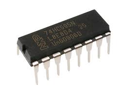
74HC595 is suitably and mostly used through its Clock, Data, and Latch pins to expand the GIPO pin-out of microcontrollers thereby increasing GIPO functionality.
Features and Specifications:
- 8-bit, Serial In – Parallel out Shift register
- Operating Voltage: 2V to 6V
- Power Consumption: 80uA
- Output source/sink current: 35mA
- Output Voltage is equal to Operating voltage
- Minimum high-level Input Voltage: 3.15V @(Vcc=4.5V)
- Maximum low-level Input Voltage: 1.35V @(Vcc=4.5V)
- Can be easily cascaded with more IC to get more outputs
- Maximum Clock Frequency: 25Mhz @4.5V
- Available in 16-pin PDIP, GDIP, PDSO packages
Applications:
- Applicable in Expanding the GPIO pin on a MCU/MPU
- Applicable in LED Matrix/Cube Projects
- Applicable in interface LCD
- Useful in cascading applications
- Useful in high logic level controller applications
Download the datasheet for more information configuration.
20. MSP432 – a 48MHz ARM Cortex-M4 family with integrated analog
MSP432 is an ultra-low-power MCU. The ARM Cortex-M4 core in this new MSP432 microcontroller platform provides a non-proprietary ARM ecosystem to MSP430 MCU users with FreeRTOS. FreeRTOS is a prime real-time kernel. The MSP432 features 1 MSPS 14-bit ADC that provides high performance, high resolution, and low power consumption. With single-ended mode, it consumes only 210uA at 1.8V and 1Msps while the differential mode consumes only 260uA at 1.8V and 1Msps. The MSP432 MCU offers a low active current of 95uA/MHz in a sensor solution used widely in industrial applications. Additionally, MSP432 is fully CMSIS compliant giving room for the development of reusable and compiler-independent code.
Features and Specifications:
- Low Supply Voltage Range: 1.8 – 3.6 V
- Address space: 32 bits
- Memory address space: 4 GB
- Clock speed: 48 MHz
- Floating Point: IEEE754 32-bit FPU
- Peripherals: internal oscillator, timer including PWM, watchdog, USART, SPI, I²C, 10/12/14/16/24-bit ADCs, brownout reset circuitry, comparators (that can be used with the timers to do simple ADC), on-chip op-amps for signal conditioning, 12-bit DAC, LCD driver, a hardware multiplier, USB, and DMA for ADC results.
- Built-in ROM driver library that facilitates software reuse.
- Redesigned interrupt mechanism, using Nested Vectored Interrupt Controller (NVIC)
- Improved resolution (14-bit) and speed (1 MSPS) ADC
- Redesigned uDMA engine
- ARM-specific SysTick and Timer32 timer/counter blocks
Applications:
- Used for low powered embedded devices
- Used in an industrial factory, industrial process, and building automation
I hope this helps in choosing the right type of components to buy for your lab. Please feel free to comment and make contributions on what you think could also be added.
Best of luck in your practices!
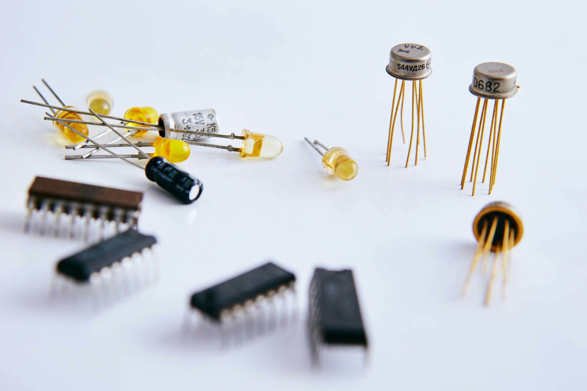
cover photo: depositphotos.com