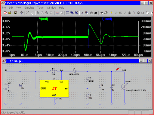
LTspice is powerful electronic circuit simulator software and it is free. Probably because it is free, not too much effort has been put into its user interface. Even though it is perfectly capable of what it is designed for, it does not look pretty and lacks user-friendliness. But with a bit of effort, it can be a valuable tool. This video will help you to get started with LTspice. As an example circuit, we use a small 1.5 V AA battery-powered circuit that blinks an LED for two years, published in the summer 2020 edition of Elektor Magazine, on page 65: https://www.elektormagazine.com/magazine/elektor-151
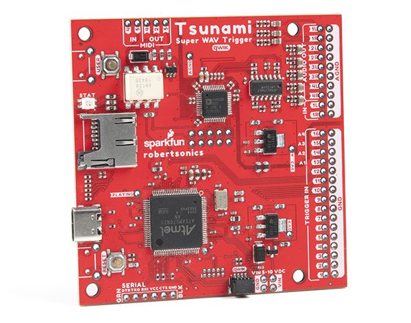
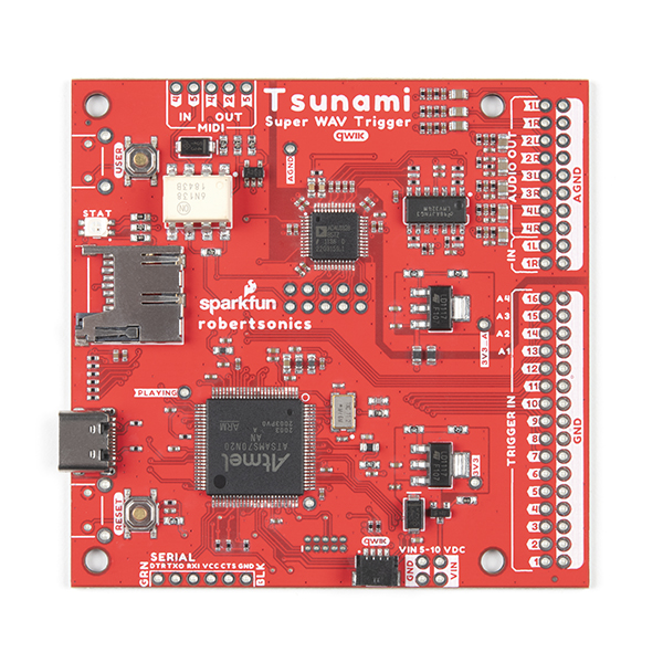
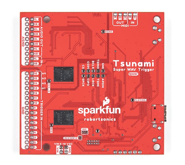
Qwiic Tsunami Super WAV Trigger is a powerful polyphonic embedded audio player designed by SparkFun in collaboration with James Robertson’s robertsonics. The super powerful audio board is capable of producing high-quality audio.
The audio board is “polyphonic,” in contrast to most other embedded audio players. This implies it can simultaneously play multiple tracks. This is done by maintaining multiple file pointers and digitally mixing the tracks to Tsunami outputs. Tracks can start at any time in polyphonic mode, regardless of what other tracks are playing, including copies of the same track. The only restriction is the number of “voices”, the number of different tracks that can be played at any given time. It currently has 18 low-latency stereo voices and 32 low-latency mono voices available.
Features of Qwiic Tsunami Super WAV Trigger
Tsunami Super WAV Trigger is built around Atmel’s high-performance ATSAMS70ARM Cortex-M7 processor. It can play 44.1kHz, 16-bit mono, or stereo.wav files (tracks) from a microSD card. Additionally, it can play up to 18 stereo or 32 mono tracks independently and simultaneously, depending on whether it is in mono or stereo mode. It also mixes them to either four stereo or eight mono line-level audio outputs.
Each track has its own volume control and can start, pause, resume, loop, and stop independently. This allows you to create the perfect interactive blend of music, dialogue, and sound effects. In addition, the board also allows for true seamless looping over any track length. The Qwiic system allows for solderless connectivity to the rest of your system. However, if you like to have complete access to each pin, the manufacturer has broken out 0.1″-spaced pins. With either 16 programmable trigger inputs, a serial control port, or a dedicated MIDI port, up to 4096 tracks can be indexed and started with low latency (typically 8ms).
What makes it even more remarkable is that the Tsunami features eight audio output channels. Thus, it can be configured as either eight mono or four stereo pairs. You can choose between mono and stereo architecture in different firmware versions. Also, the mono version has a new “Synced Set” trigger feature that can initiate up to eight mono tracks on adjacent outputs.
With a single trigger, these tracks will start and stay in sample sync for playing stereo or even 5.1 or 7.1 surround sound content. Hence, any track routes to any output in a dynamic manner. Furthermore, each output offers independent real-time volume and sample-rate conversion.
Tsunami is also compatible with other microcontrollers, such as Arduino. A serial control port, combined with a robust serial control protocol, allows you to access all 4096 tracks and use Tsunami’s internal faders for real-time mixing, crossfading, and pitch bending. All of Tsunami’s functionality can be accessed from within your Arduino sketch using an Arduino Serial Control Library.
Product Showcase of Qwiic Tsunami Super WAV Trigger
Discussing further, the board features a dedicated MIDI port with an integrated optoisolator. This port makes it easy to connect to your MIDI keyboard or any MIDi controller. It supports MIDI note-on, note-off, pitch bend, and program changes messages, and controller messages for controlling sustain, attack, and release times, and volume in real-time. Even if you run out of voices, a voice-stealing algorithm ensures that new notes are played. Talking about the software support, the board can be programmed using the Arduino IDE or Python, and it can also be controlled through serial.
The Qwiic Tsunami Super WAV Trigger board is available on SparkFun at $79.95. For more information visit the official product page. Images and technical specifications have also been taken from the product page.
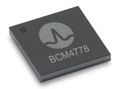
Broadcom Inc. today announced the world’s lowest power L1/L5 GNSS receiver chip, the BCM4778, optimized for mobile and wearable applications. Equipped with the latest GNSS innovations, this third-generation chip is 35% smaller and consumes 5 times less power than the previous generation.
Dual-frequency GNSS continues to be an important location feature for modern mobile and wearable devices as it provides greater positioning accuracy for location-based services (LBS) applications. The advanced L5 signal enables sidewalk-level accuracy for pedestrian navigation in urban environments, as well as lane-level accuracy for vehicle navigation.
Reduction in GNSS power consumption is crucial to extending the battery life of a mobile or wearable device. Compared to GNSS receivers used in integrated platforms, Broadcom’s single-chip BCM4778 delivers significantly lower power consumption and higher performance while offering more advanced GNSS features, such as the next-generation Grid Tracking™ urban multipath mitigation technology. Further, the BCM4778 increases the GNSS always-on battery life on a smartwatch by 30 hours when compared to the previous generation chip operating on a 300mAh battery. The extended battery life benefit helps drive new experiences in smartwatches and phones. For example, smartwatches can keep the GNSS always-on for fitness applications for multiple days on a single battery charge.
In addition, the BCM4778 features fully integrated LNAs for L1 and L5 bands, which reduces RF front-end BOM costs and footprint requirements, ideal for space-constrained applications. The chip offers immense flexibility to smart watch and phone designers with its small size. Having the ability to place the BCM4778 closer to the antenna helps improve signal reception and thereby enhances the overall GNSS performance.
Product Highlights
7nm CMOS technology
Typical power consumption
4mW L1 band only
6mW L1+L5 simultaneous
FCBGA package
New Grid Tracking™ technology
Advanced multipath mitigation
Continuously tracks the full L5 channel
Capable of L5 acquisition
Increased processing capability and throughput
Advanced LTE filtering and jamming mitigation
Enhanced LTE Band 13 and Band 14 filtering
Spoofing and jamming detector
Jamming mitigation through multiband and multi constellation
Reduced BOM cost and footprint
Flexibility in using internal LNAs
Optional operation without interstage SAW filters
Integrated switching regulator with direct connect to battery
“With the launch of this third generation dual-frequency GNSS receiver chip, Broadcom continues the tradition of raising the bar for mobile GNSS,”
said Vijay Nagarajan, vice president of marketing for the Wireless Communications and Connectivity Division at Broadcom.
“Always-on dual frequency GNSS is a key request from mobile and wearable OEMs, and we are thrilled to deliver it.”
“We are excited to see this impressive power reduction, combined with the L5 Grid Tracking technology in the new Broadcom GNSS chip. This will increase the impact of Google’s 3DMA ray-tracing for urban multipath mitigation,”
said Frank van Diggelen, the principal software engineer at Google.
“Consumer electronic companies have been faced with the challenge of managing power consumption versus performance, often having to choose one over the other. Broadcom’s innovative approach to the BCM4778 allows their customers to realize improvements on both fronts,”
said Ramon T. Llamas, research director for mobile devices at IDC.
“The result: device manufacturers can enable new experiences and run applications over a sustained period of time. In addition, by reducing its BOM cost and its physical footprint, Broadcom is enabling further benefits from cost savings and design configurability.”
Availability
Broadcom is currently sampling the BCM4778 to its early access partners and customers. Please contact your local Broadcom sales representative for samples and pricing.
Targeting Internet of Things Sensing Networks, NevadaNano will show the Mini Flammable in booth #733 at Sensors Converge this week, September 21 through 23.
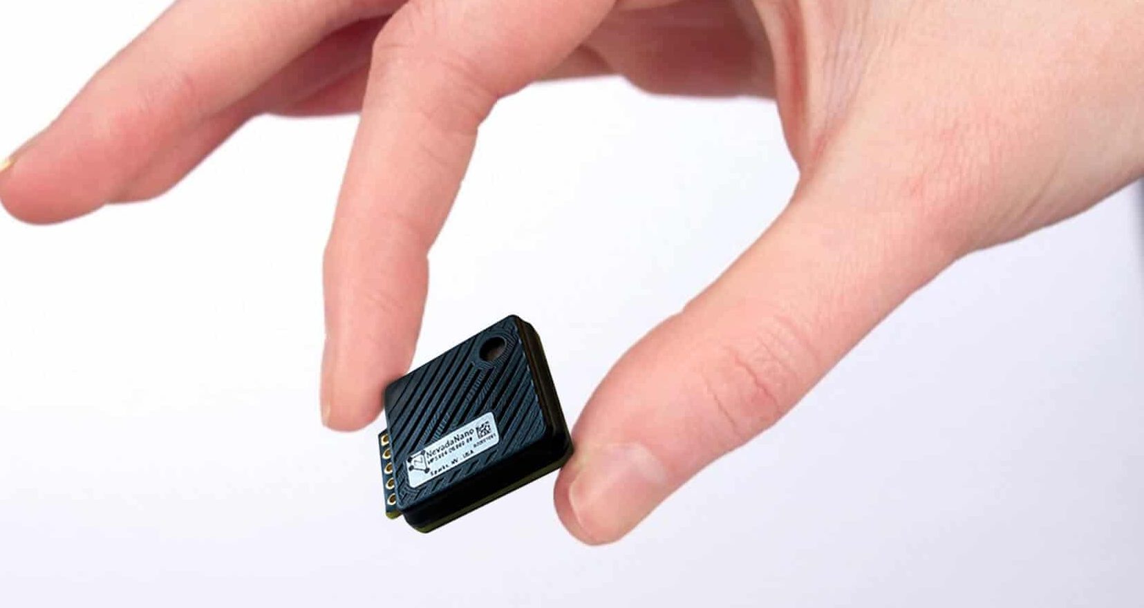
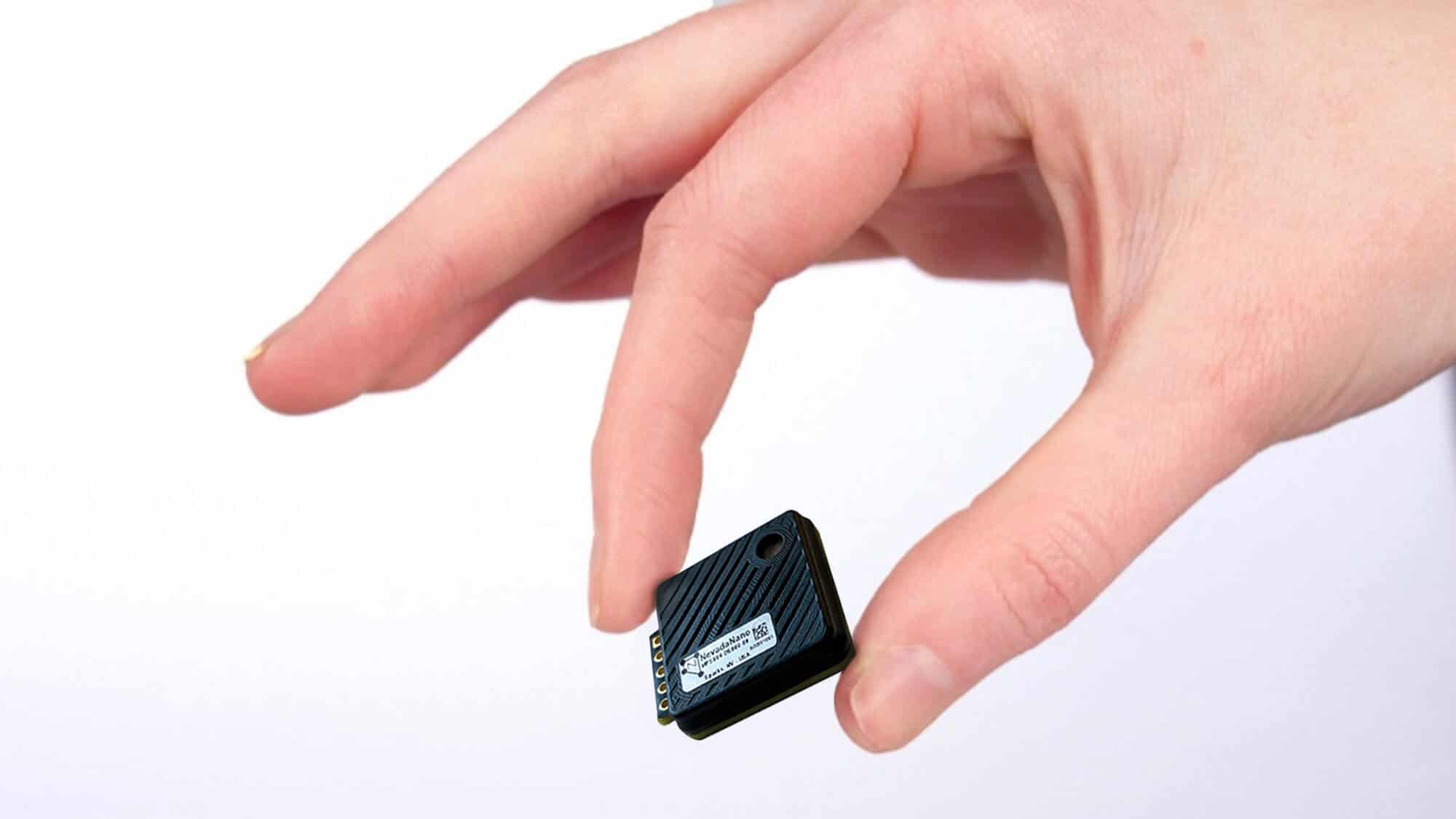
NevadaNano, the world’s leading gas detection sensor technology innovator, today announced the “MPS™ Mini” a miniaturized version of the highly popular Molecular Property Spectrometer™ (MPS™) Flammable Gas Sensor. The new sensor is the world’s most accurate hydrocarbon sensor in its class and eliminates the need for maintenance during its 10+year lifetime. The sensor will debut this week at Sensors Converge in Booth #733.
“We have extended our market-leading reliability, accuracy, and lifetime with enhanced algorithms which extends our market-leading position of detecting 19 of the most common combustible gases found in residential, commercial, and other general use environments,”
said Ralph Whitten, President, and Member of the Board of Directors, at NevadaNano.
“This new product in a lower cost package specifically targets IoT and high volume applications. This enables our customers to set new standards in connected gas sensors and helps companies create safer working environments in industrial, commercial and consumer applications.”
The newest addition to NevadaNano’s MPS product family, the MPS Mini Flammable gas sensor measures the thermodynamic properties of the air-gas mix and accurately reports 0-100% LEL across 19 flammable gases without the need for field calibration. This performance meets the need for flexible sensor platforms in a wide range of non-industrial applications and makes it ideal for residential and commercial applications like smart meters and IoT devices. In essence, the Mini Flammable creates safer environments for people and their surrounding communities.
Integrated, real-time measurements and built-in compensation for temperature, pressure, and humidity enhance the accuracy of all NevadaNano’s MPS flammable gas sensors. Gas concentration readings are accurate across the entire environmental range, including rapid environmental transients, delivering best-in-class accuracy. The Mini Flammable, like all MPS sensors, is inherently immune to drift, decay, or poison.
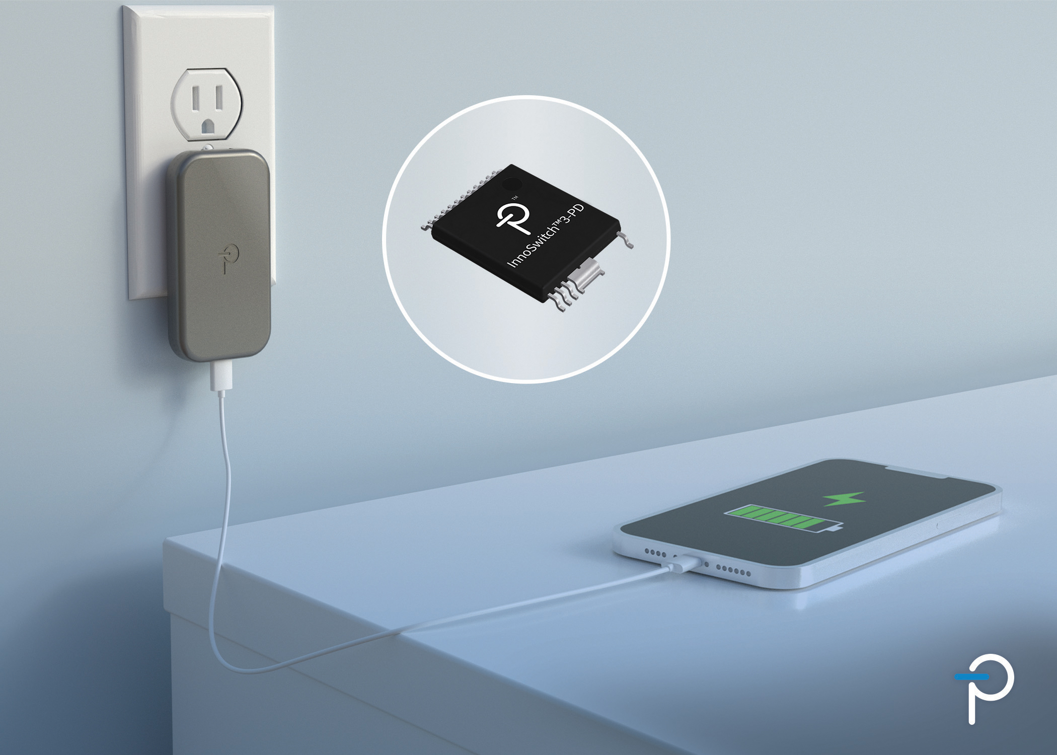
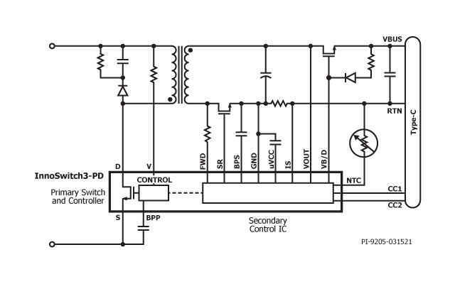
A fully integrated charger solution combines USB PD, PPS, PowiGaN and FluxLink to maximize efficiency and slash component count in adapters and chargers
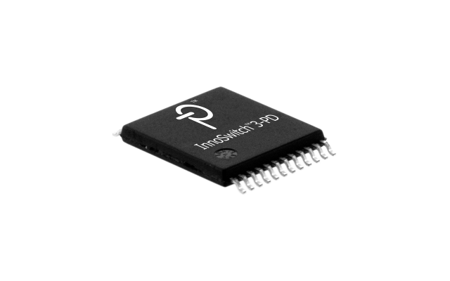
Power Integrations, the leader in high-voltage integrated circuits for energy-efficient power conversion, today announced the InnoSwitch™3-PD family of ICs, the industry’s most highly integrated solution for USB Type-C, USB Power Delivery (PD), and USB Programmable Power Supply (PPS) adapters. This compact InSOP™-24D-packaged IC includes a USB-C and PD controller, a high-voltage PowiGaN™ switch, a multi-mode quasi-resonant flyback controller, secondary-side sensing, FluxLink™ isolated digital feedback and a synchronous-rectification driver.
Aditya Kulkarni, senior product marketing engineer at Power Integrations said:
“InnoSwitch3-PD ICs target designers seeking the ultimate in charger power density. This requires the highest level of integration and maximum efficiency to limit self-heating. Our latest addition to the InnoSwitch3 family dramatically simplifies the development and manufacturing of compact, energy-efficient USB PD power supplies for smartphones, tablets, notebooks, and other devices that benefit from fast charging. InnoSwitch3-PD ICs reduce the BOM count to half that of conventional designs, reducing design time and simplifying high-volume manufacture for slim, ultra-compact OEM and aftermarket chargers.”
Featuring no-load power consumption as low as 14 mW, power supply designs using InnoSwitch3-PD ICs meet all global energy-efficiency regulations. The high efficiency of these devices ensures low heat dissipation, eliminating the need for bulky heatsinks. Power Integrations’ FluxLink high-speed communications feedback link ensures fast, accurate secondary-side regulation. InnoSwitch3-PD ICs are also fully protected, with input voltage monitoring, accurate brown-in/brown-out and overvoltage protection, and output over- and under-voltage fault detection with independently configurable fault responses.
Availability & Resources
A new design report, RDR-838, describes a 60 W USB PD 3.0 Power Supply with 3.3 V – 21 V PPS output using the InnoSwitch3-PD PowiGaN-powered INN3879C-H801. The new InnoSwitch3-PD ICs are priced from $1.30 per unit in 10,000-unit quantities. For further information, contact a Power Integrations sales representative or one of the company’s authorized worldwide distributors: Digi-Key, Farnell, Mouser and RS Components.
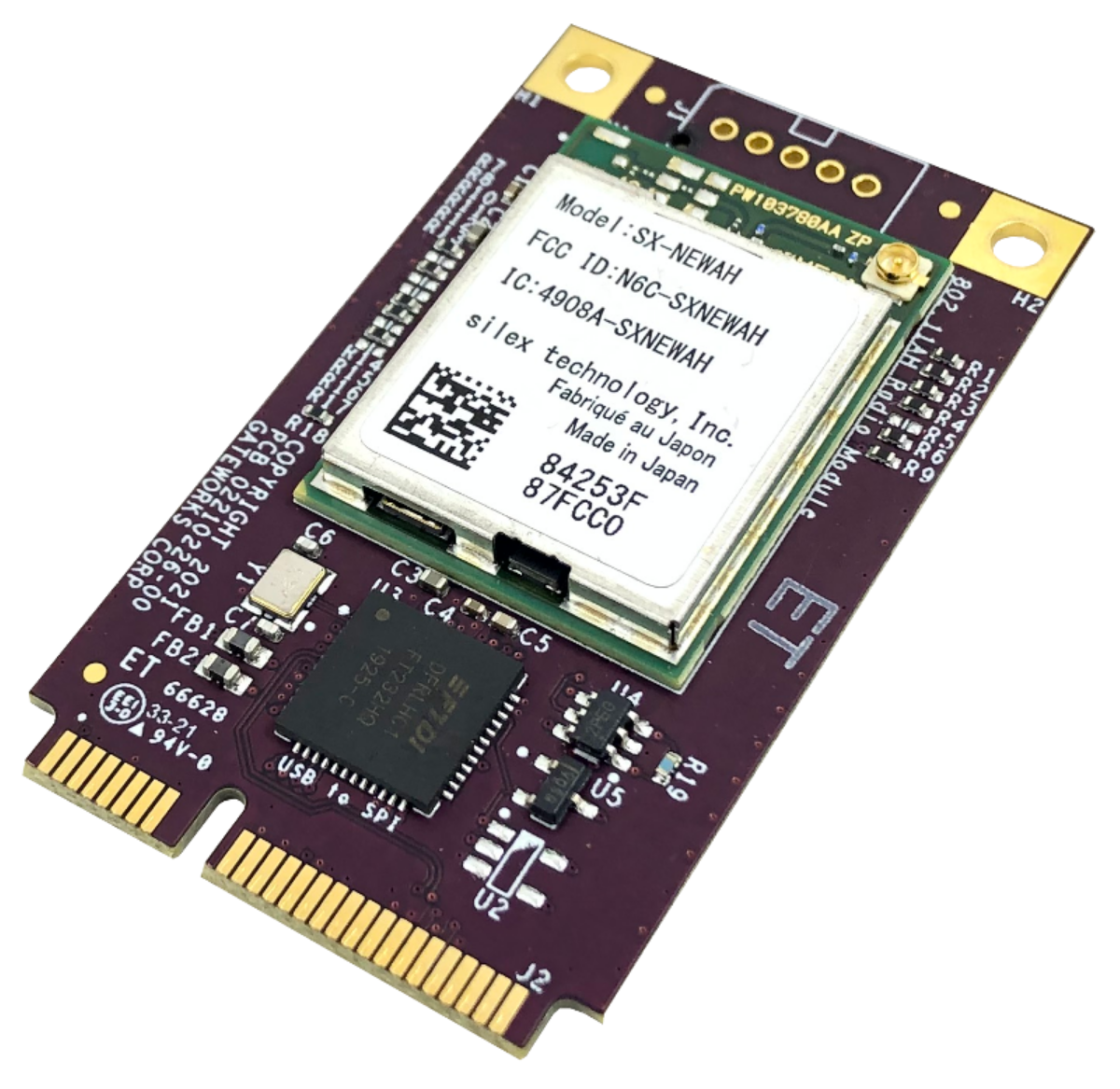
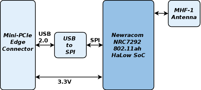
Gateworks is proud to announce the GW16146802.11ah HaLow Mini-PCIe radio for the industrial internet of things (IoT) applications. It uses the Silex SX-NEWAH module, which is based on the Newracom NRC7292 System-on-Chip. The GW16146 brings all the advantages of 802.11ah to the Gateworks rugged and industrial single board computers.
802.11ah, often called Wi-Fi HaLow, is a new standard that uses Sub-1GHz frequencies to provide a longer range at lower power consumption. It can support 1000’s of clients with WPA-3 security. By utilizing a standard TCP/IP framework, no special code or SDKs are required. With everything being open source and unlicensed, no costly consortium memberships are required.
802.11ah HaLow Mini-PCIe Radio Highlights:
Long Range
Unlicensed frequency band – Sub 1-GHz
Standard TCP/IP Framework – No special software is needed
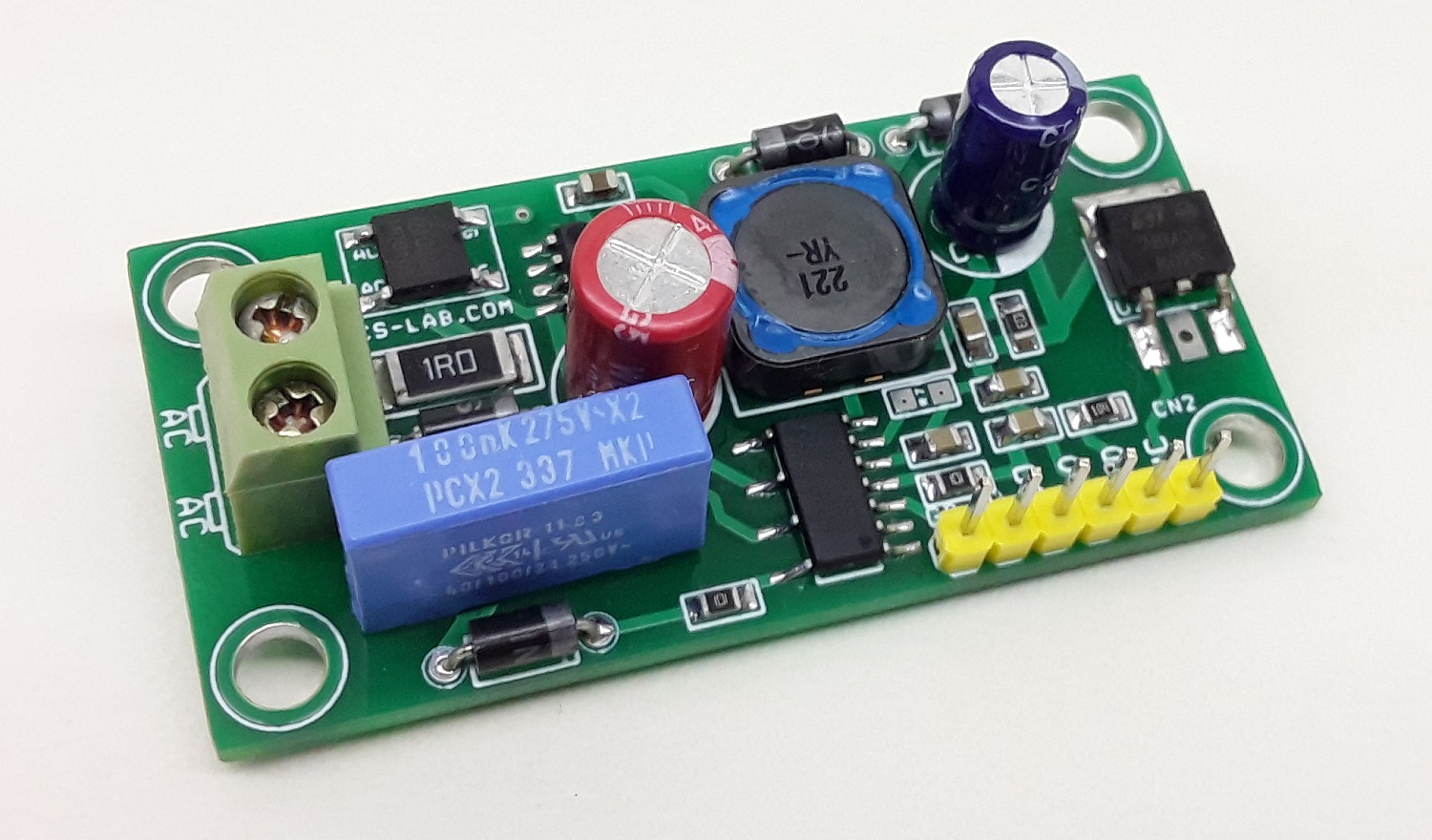
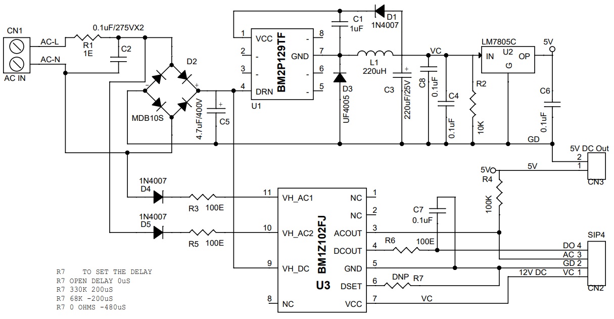
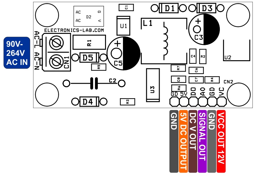
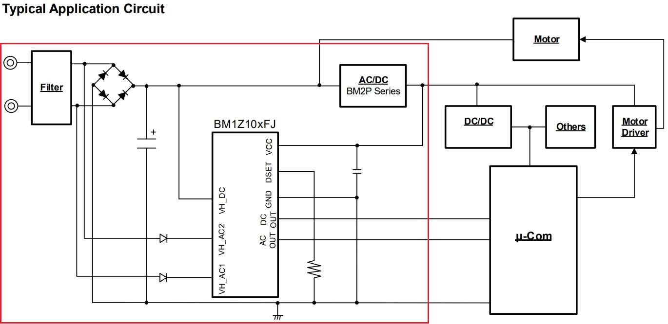
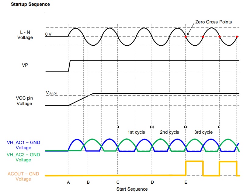
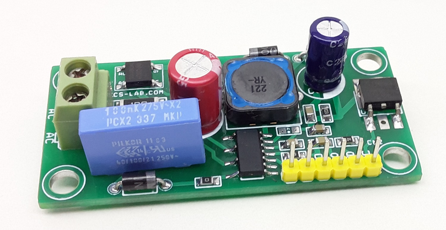
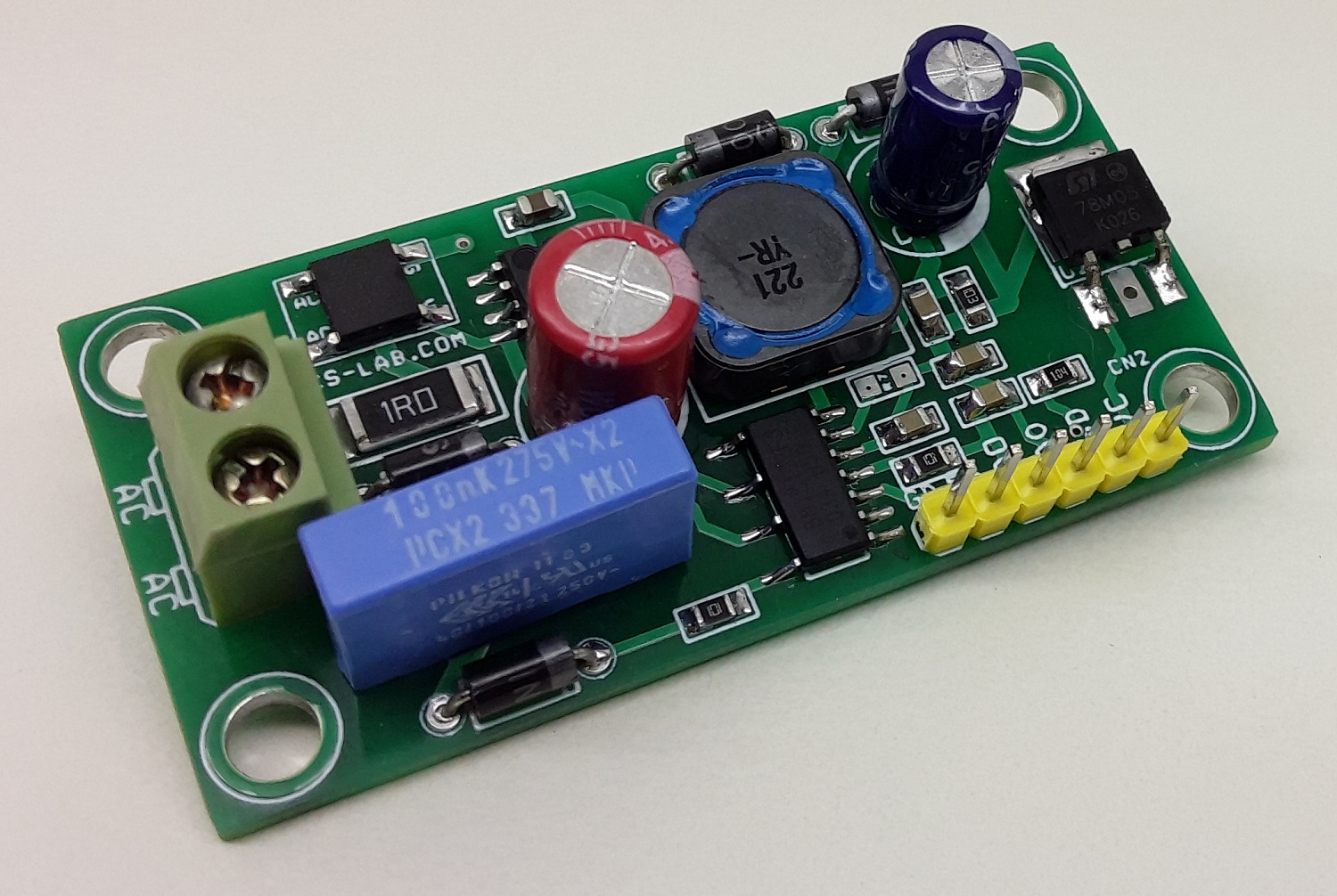
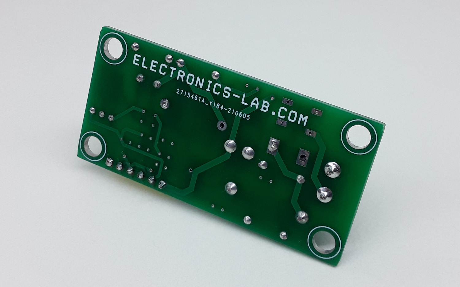
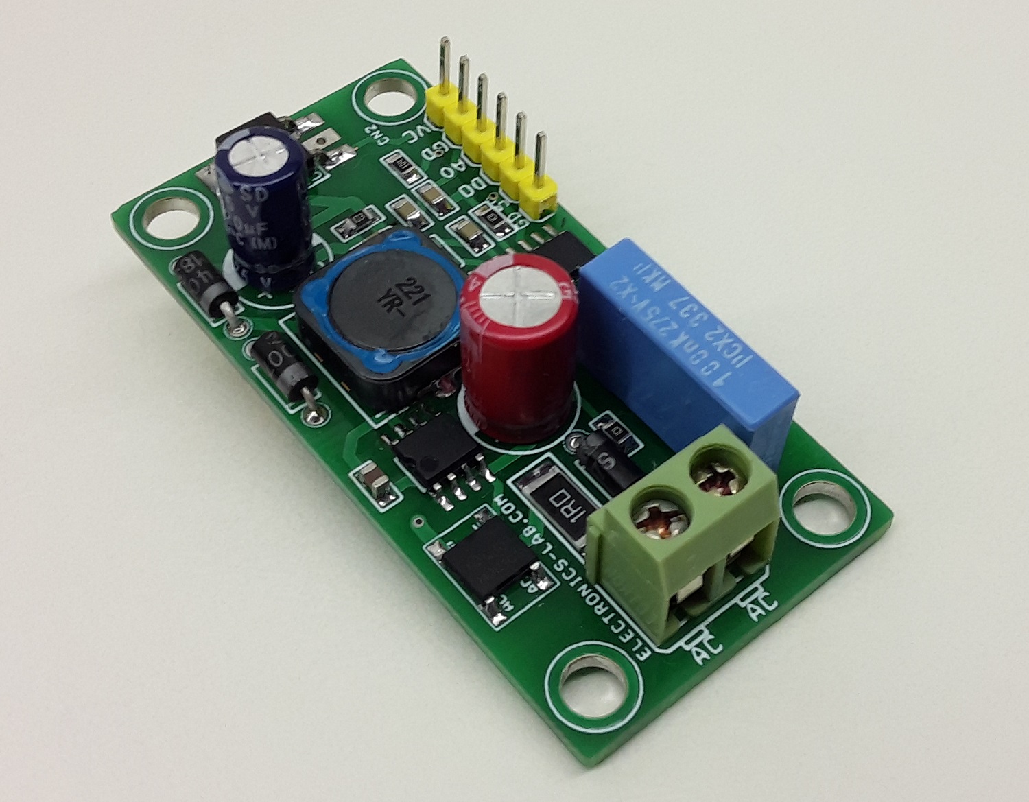
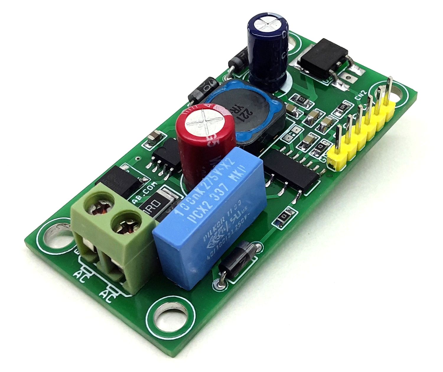
This project provides AC voltage zero-cross timing detection and a DC voltage after diode rectification with high accuracy. Possible applications for such circuits are AC motor controllers, AC lamp controllers, AC Dimmer Controllers, Home Appliances. The circuit outputs a zero-cross signal from 90 Vac to 264 Vac input. The project is based on BM1Z102FJ chip which outputs a high precision zero-cross timing of targeted AC voltage and a DC voltage after diode rectification of high accuracy. The project also includes high voltage offline AC to DC converter chip BM2P129TF.
AC Voltage Zero Cross Detection
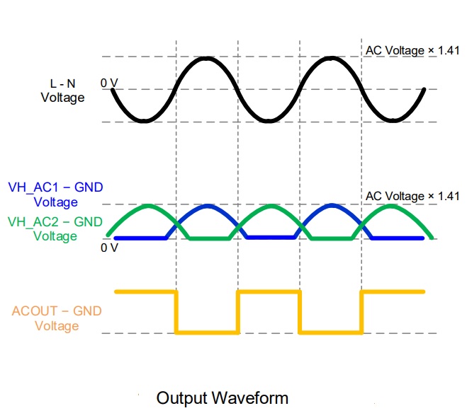
By monitoring the voltage between the VH_AC1 and VH_AC2 pins, this IC outputs the zero-cross point of AC voltage from the ACOUT pin. These pins have a built-in monitor circuit that tolerates 600 V and they realize high reliability and low power consumption. The ACOUT pin performs an N channel open-drain output and this makes it possible to support various applications. It is necessary for the VH_AC1 pin to be connected to the N side of the AC input and for the VH_AC2 pin to be connected to the L side of the AC input
Note: The circuit operates with potentially lethal voltages, it is advisable to use an isolated probe for measurement using an oscilloscope
This board works with mains high voltage contains lethal voltage and should be handled only by qualified personnel familiar with all safety and operating procedures. Board contains parts that store significant charges even after disconnecting from the power source. Please discharge the capacitors after using the board, and please deal with it after confirming such electric discharge.
Be careful to not allow conductive objects to come into contact with the board. DO NOT touch the board with your bare hands or bring them too close to the board. In addition, as mentioned above please exercise extreme caution when using conductive tools such as tweezers and screwdrivers.
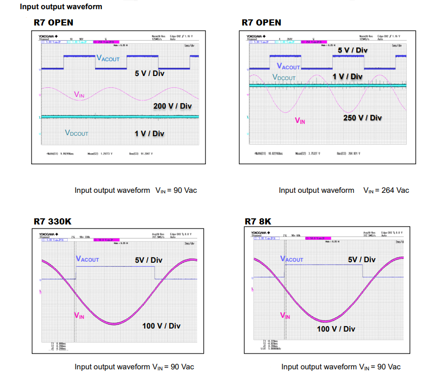
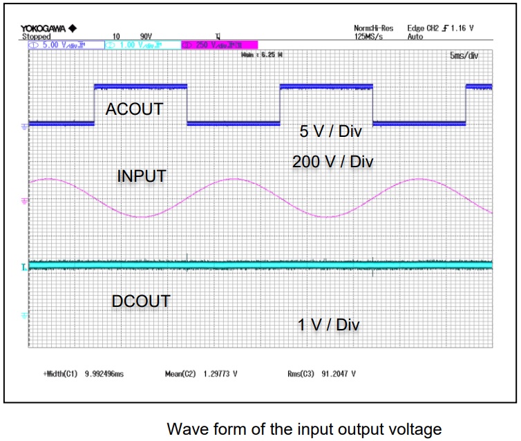
Input-Output Waveforms
Features
Supply Input 90V AC to 264V AC
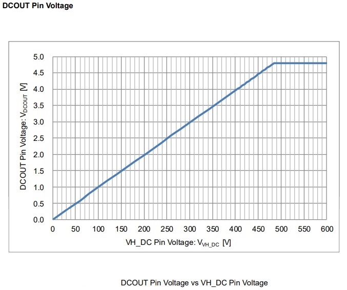
On Board AC to DC Offline Converter (90VAC-264V AC input, 12V DC Output @ 100mA)
DC Output about 1/100 voltage Approx. 1.1V with 110V AC, 3.3V with 230V AC input
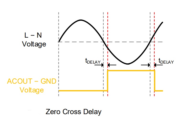
Input Frequency Response 47Hz to 63Hz
Provides Accurate 50Hz Square wave with 230V/50Hz AC Input
Default Output Pulse Delay time = 0uS (Can be Adjust Using R7)
Aux DC Supply Output VCC-12V and 5V DC @ Maximum Load 100mA
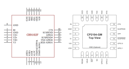
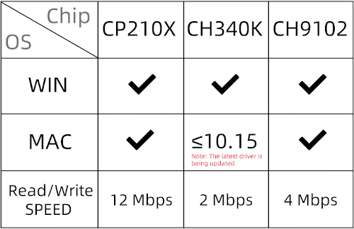
As the applications of USB interfaces on computers, MCU boards, devices, and other I/O peripherals increases, there’s a parallel increase in demand for cost-effective and high-power USB bus converters for serial and parallel interfaces. CH9102F, a low-cost USB to high-speed serial port chip manufactured by Nanjing Qinheng Microelectronics, is one of such.
The CH9102F is a CH9102 family of USB to single serial port chips that features a full-duplex serial port, transceiver buffer, and a maximum baud rate of 4Mbps. The chip supports an operating voltage of 3.3 – 5V and serial port I/O interface signals of 1.8 – 5V range, as well as support RS232 and RS485 interfaces. The chip is also compatible with modem interface signals: CTS, DSR, RI, DCD, DTR and RTS, defined and controllable by computer/user application which makes it a versatile and flexible chop for professional and DIY projects.
The CH9102F comes as a 4x4mm ultra-small square with 24 pins, supporting 485 direction control, a built-in crystal oscillator, built-in power-on reset, and a USB 2.0 interface. It features an EEPROM, configurable with chip VID, PID and other relevant parameters that can be seen on its datasheet. Going further, when compared to CP2104, apart from lower cost, the CH9102F has 6 GPIO pins while the former has 4 GPIOs with similar pin-outs. For makers, these extra pins make an advantage allowing for more peripheral expansion. This is a big reason it should be a favorite chip to makers, DIY users, and hobbyists alike.
image source: www.cnx-software.com
Features and Specifications
The features of the chip gotten from its datasheet are given below:
Power supply: 3.3 – 5V
A full-speed USB device interface, USB 2.0 compatible.
Serial port interface I/O powered independently, supports 5V, 3.3V, 2.5V, 1.8V power supply voltage.
A built-in firmware, which emulates a standard UART interface, is used to upgrade the original serial peripherals or expand additional serial UART via USB.
Its original serial applications are compatible without any modification.
It supports a free-installation operating system built-in CDC driver or multi-functional high-speed VCP manufacturer driver.
It has hardware full-duplex serial UART interface, integrated transmit-receive buffer, supports communication baud rate varies from 50bps to 4Mbps.
It supports 5, 6, 7 or 8 data bits, supports odd, even, blank, mark and no parity.
It supports common MODEM interface signals RTS, DTR, DCD, RI, DSR and CTS.
It supports CTS and RTS hardware automatic flow control.
Supports half-duplex, provides sending status TNOW supports RS485 switch.
Provides further RS232 interface, through external voltage conversion chip.
Built-in power-on reset, built-in clock, no external crystal required.
RoHS compliant QFN24
On the software part, the CH9102F runs on a high-speed virtual COM port (VCP) manufacturer’s driver or a free-installed OS built-in communication device class (CDC) driver. It supports CTS/RTS hardware flow control protocol to handle frame collisions during data transfer.
Applications:
To expand the UART interface of the computer and MCU.
To upgrade serial devices: MCUs to the USB bus.
USB to RS485 conversion.
USB to RS232 conversion.
USB to TTL serial port conversion.
CH9102F is available for purchase on 1688 for ¥5.50.
For further information and configurations, download the datasheet.
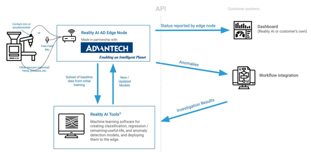
Reality AI recently announced RealityCheck AD at Sensors Converge Expo 2021 in partnership with Advantech. It provides advanced Anomaly Detection (AD) for equipment monitoring and end-of-line testing. It comes with Edge Node hardware from Advantech or RasPi, Reality AI Edge Node firmware, Reality AI Tools machine learning software, and several sensors to choose from.
Talking more from the software perspective, Reality AI combines advanced signal processing with Artificial Intelligence on inexpensive processors. To derive a custom transform depending on time and frequency, Reality AI employs an algorithmic search of a wide variety of feature spaces. Moreover, the code runs on ARM M- R- A-, and non-ARM microcontrollers, as well as on Intel processors and Linux
What is Anomaly Detection?
Anomaly detection refers to the detection of some abnormal data or information which is different from the normally expected data. Intrusion detection, fraud detection, fault detection, system health monitoring, event detection in sensor networks, identifying ecological changes, and defect identification in pictures using computer vision are all examples of anomaly detection. Anomaly detection is also important to monitoring the proper functioning of industrial equipment and conducting quality control inspections.
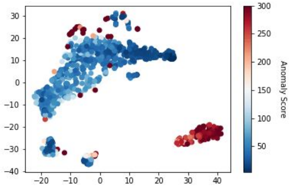
Anomaly Detection methods find a baseline normal region in a feature space using one of several different machine learning algorithms. Then scores are calculated for each observation that provides a measure of how “far away” that observation is from the normal baseline region in that feature space. The “farther away” that observation is, the less like normal it is. By applying a threshold to these scores, you can declare observations that are “too far from normal” to be anomalous.
Sample 2D projection of multidimensional feature space, with observations that have anomalous and normal scores color-coded. Typically, normal points are clustered in a compact region, with multiple clusters of anomalies well separated, and a “fog” of anomalous points around the space
Performing AD in the right way
The wrong ways of doing anomaly detection include building AI models with very little or no data on known anomalies. For an efficient model, there must be a sufficient amount of anomalous data. If such kind of data is not available, a few anomalies can be created for testing.
Also, gathering and testing in limited and controlled circumstances must be avoided. Instead, data should be gathered and tested continuously in a wide range of conditions, while screening out false positive and false negative values as they can affect the efficiency of the model.
Moreover, some instruments can miss some important data that matters the most. Hence, using sophisticated sensors or instruments for gathering rich quality data is important. Also, try to include metadata wherever possible.
RealityCheck AD for Efficient and Easy Anomaly Detection
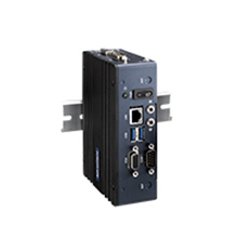
The RealityCheck AD offers a complete hardware and software solution for AI-driven, machine-level analytics for a factory or any product. It includes a self-learning edge node which is a rail mountable edge unit manufactured by Advantech. The RealityCheck AD Edge Node is based on the Advantech EPC-S201 embedded PC. It features an Intel Celeron N3350 Dual-Core SoC with 8GB RAM and 64GB SSD. It offers wi-fi, wired ethernet, and cellular connectivity.
Sensor options available for interfacing include:
Industrial-grade accelerometers – relatively high cost, but hardened with standard machine mounts and tight tolerances.
Lower-grade accelerometers – cheaper, with wider tolerances and lacking industrial hardening, but still sufficient for many tasks
Current and Temperature sensors
Contact Microphones – similar to an accelerometer, but with very high sample rates. Usually not available in industrial packaging, but still useful for many applications.
Free-standing microphones – for capturing ambient sounds and noise events.
Explosion-proof options are available.
RealityCheck AD also comes with Reality AI Tools® software for automatic generation of machine learning models for anomaly detection, signal processing & classification, and remaining useful-life predictions.
Key Features and Advantages of RealityCheck AD
The Edge Node learns “normal” automatically and starts detecting anomalies.
Edge Node can be taught “idle” so that unproductive equipment time can be tracked accurately
Any anomalies are shown on a dashboard and captured for future investigation, analysis, labeling, and use in model development. Over time, this data can be used to create detectors for specific conditions and to predict the remaining-useful-life of components.
Generates results in a short period, improving the results over time with feedback.
Easily integrates with Manufacturing Information Systems, dashboards, and workflow management systems using MQTT.
RealityCheck AD Architecture
Firstly, the data is gathered through various sensors like contact mic, accelerometer, temperature sensor, pressure sensor, etc. These sensors are interfaced with the Reality AI AD Edge Node that is based on the Advantech EPC-S201 embedded PC. This data is then processed by the Reality AI Tools software. It uses machine learning algorithms for creating classification, regression, correlation, and anomaly detection models, and deploying them to the edge.
Based on the baseline data, it quickly detects any abnormal observations. After detecting anomalous data, the edge node reports the status to the user via an illustrative and user-friendly dashboard. Also, the detected anomalies can be used for workflow integration by investigating the anomalous data and giving feedback to the model for improving its performance. Over time, it can perform more detailed detection of specific conditions and even predict anomalies before they occur. You can visit the official page of RealityCheck AD for detailed information.
Conclusion
The RealityCheck AD by Reality AI in partnership with Advantech provides a complete solution for industrial equipment monitoring and end-of-line testing. Numerous sensors integrated with the edge node gather data and start detecting anomalies based on the baseline data automatically. Moreover, it also provides a convenient and user-friendly API for integration with dashboard and workflow systems. It is a gamechanger in the field of industrial equipment monitoring and end-of-line testing.
RealityCheck AD solution will be showcased in the Sensors Converge event this month and Auto Tech Science Fair in October. Consider registering for these events for similar hardware solutions.
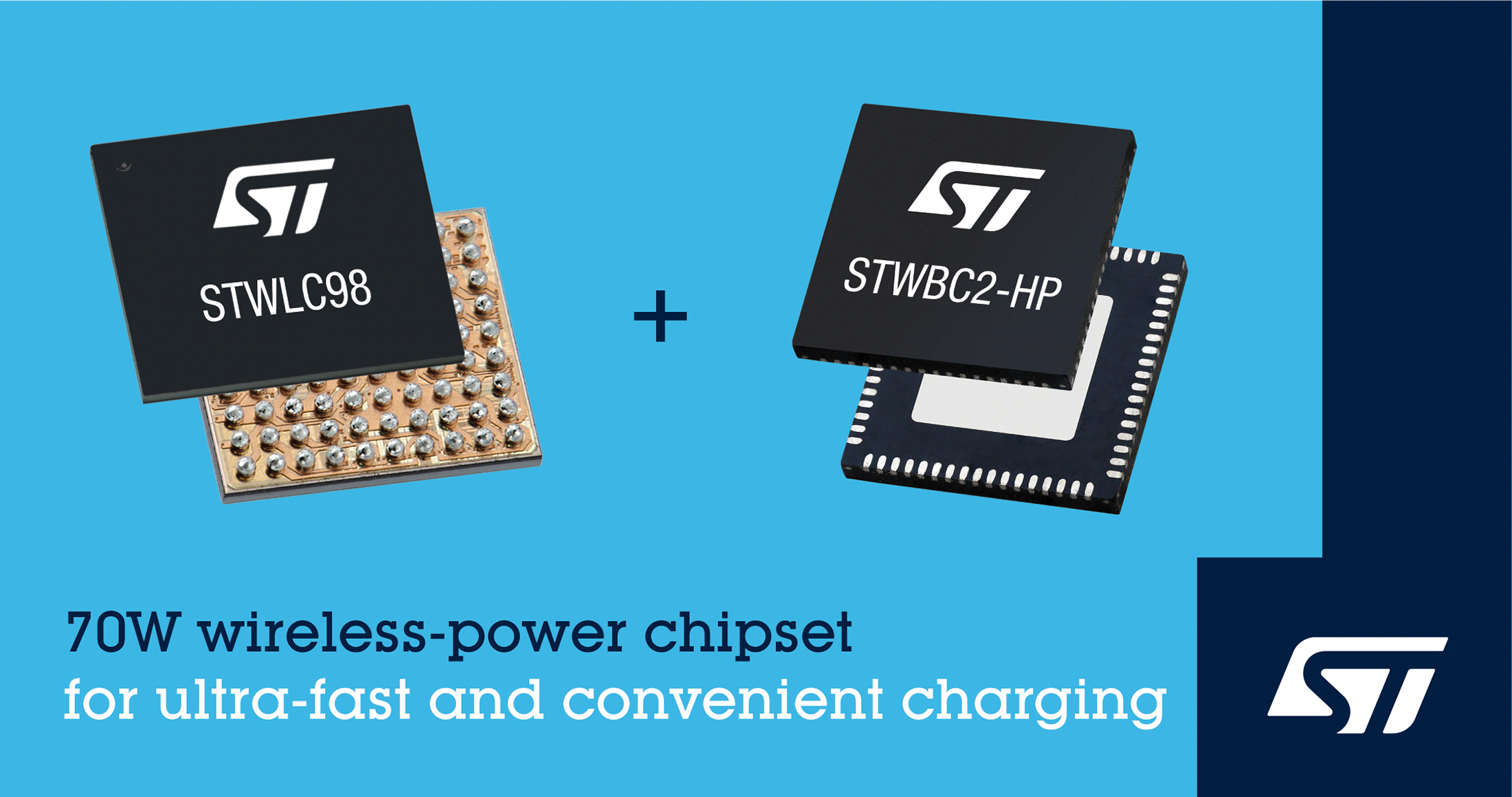
STMicroelectronics’STWLC98 integrated wireless power receiver delivers faster wireless charging and flexible charge sharing for diverse portable and mobile devices for home, office, industry, healthcare, and in-car applications. When combined with the STWBC2-HP transmitter IC, the complete transmitter-receiver system can deliver up to 70 W on the receiver end at high system efficiency.
The STWLC98 can fully charge today’s high-end smartphones, which contain high-capacity batteries, in just under 30 minutes. In addition, the new device extends opportunities for ultra-fast and convenient charging, free of cables, sockets, and restrictive connections, to a host of new applications and contexts. Moreover, contactless charging lets product creators simplify enclosure designs, reducing cost and complexity while encouraging new slimline styles and eliminating problems associated with the socket such as contamination.
Compliant with the Qi EPP 1.3 wireless-charging standard commonly used in the smartphone industry, the STWLC98 is managed by a 32-bit Arm Cortex-M3 core that supports a range of rich features including built-in protection; it comes with an embedded OS that simplifies Qi 1.3 standalone certification. On the transmitter side, the STWBC2-HP can work with ST’s STSAFE-A110 secure element to store official Qi Certificates and provides authentication that leverages state-of-the-art cryptography. Support for the Company’s innovative ST Super Charge (STSC) protocol enables fast-charging up to the maximum power transfer rate of 70 W.
The STWLC98 features ST’s proprietary Adaptive Rectifier Configuration (ARC) mode that enhances the ping-up and power transfer spatial freedom of the system in both horizontal and vertical directions without any change in hardware or coil optimization. Enabling ARC mode, which transforms the whole surface of the transmitter as a usable charging area, increases the ping-up distance by up to 50 % in all directions.
The STWLC98 works directly with the STWBC2-HP, which contains a USB-PD interface, digital buck/boost DC-DC converter, full-bridge inverter, three half-bridge drivers, and voltage, current, and phase sensors. Controlled by a Cortex-M0+ core, the STWBC2-HP executes a patented fast PID loop and also supports the STSC protocol.
ST’s new 70 W wireless-charging chipset creates a scalable solution that can be deployed in devices like smartphones, tablets, laptops, power banks, True Wireless Stereo (TWS) devices, Bluetooth speakers, and AR/VR headsets. Designers can also extend fast and convenient wireless charging to medical equipment like monitors and medicine pumps, as well as cordless power tools, mobile robots, drones, and e-bikes. The chipset is also suited to automotive applications including in-cabin charging solutions and wireless charging of various modules onboard the vehicle.
With built-in power management, the STWLC98 has an energy-saving ultra-low-power standby mode while total end-to-end charging system efficiency can exceed 90 %, thereby complying with stringent eco-design targets. The power charger chip features dedicated hardware and advanced algorithms that were developed to address challenges in ASK and FSK communication during high power delivery. Safety features include foreign object detection (FOD), which leverages high-accuracy current-sense IP, Q-factor detection, and robust communication between transmitter and receiver.
As an additional feature that gives users extra flexibility, the STWLC98 can also operate in high-efficiency transmitter mode to allow high-power charge sharing between devices. This is coupled with the STWLC98’s industry-first embedded Q-factor detection in a receiver device to ensure safe operation in transmitter mode.
Users of ST’s wireless power solutions can download and benefit from the free PC-based graphical tool, ST Wireless Power Studio, to accelerate design-in and simplify processes including calibrating FOD, tuning Q-factor detection, and communication diagnostics. Both devices are in high-volume mass production. The STWLC98 is packaged as a 4.3 x 3.9 x 0.4 mm 90-bump WLCSP and the STWBC2-HP is available in 8.0 x 8.0 x 0.4 mm VFQFPN-68 package.