Automated X-RAY Inspection System by PCBGOGO

When you consider the cost, time, and other resources that go into PCB Design and Manufacturing, you will agree that it makes perfect sense to leave no stone unturned in ensuring quality because failure at any point could cost product owners a lot of reputation, money and time, which most companies don’t have, thanks to the strain that comes with manufacturing hardware.

While this ultimately starts from the design process, the final buck usually rests on the PCB manufacturer who takes extra effort to conduct a number of tests and processes that help to implement PCB quality control, one of which is PCB inspection.

PCB inspection is usually done to detect likely defects like foreign matter, copper explosion, scratch, insufficient plating, incorrect silkscreen, uneven solder paste and pads, residual copper, and imaging. Most PCB manufacturers use the traditional naked eye inspection method to achieve this, while some others make use of some visual inspection devices like a magnifying glass, and AOI (Automated Optical Instrument), a solder paste inspection equipment, or an optical video display system that combines both the naked-eye inspection and the AOI methods, just to mention a few.

Some of these methods actually merit more than the others, but when it comes to PCB quality control inspection, the choice of the method depends on the particular inspection test to be carried out.

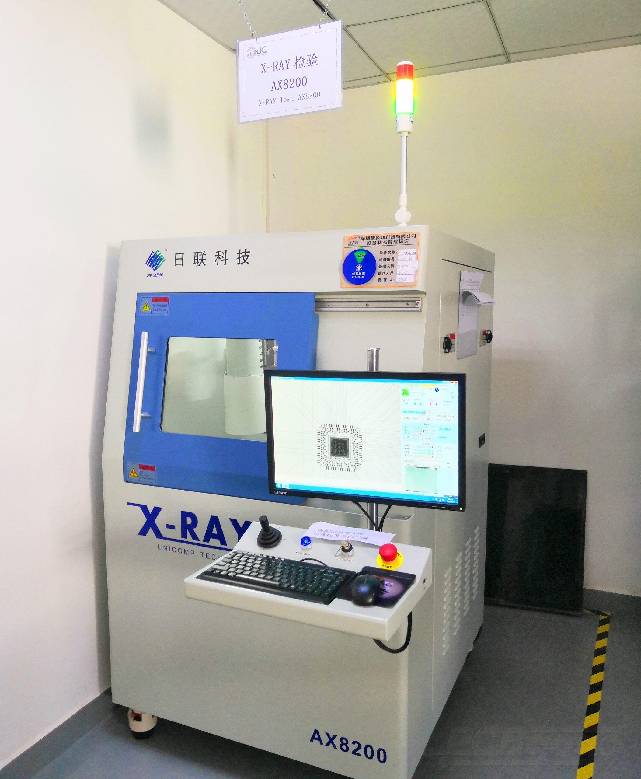
Automated X-ray inspection

Since many PCBs today now use technologies such as BGA, BGA ICs (integrated circuits), and CSPs (chip-scale packages) where the solder connections are not visible by visual inspection, like naked eye or ordinary optical systems, it is now necessary to carry out checks using X-ray technology.

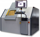
Automated X-Ray Inspection is one of the most reliable inspection technologies used by PCB manufacturers to further improve manufacturing quality. It is the perfect inspection method for detecting defective solder joints or faulty melting of the solder and it works well for BGA components and other small-footprint devices.

AXI runs on the same principle as the Automated Optical Inspection (AOI) but uses computer vision with x-ray images instead of visible light for detecting defects. With this, the system can inspect and validate all the solder connections that were made on the board after assembly, including those hidden underneath a component.

Working Principle of An Automated X-ray Inspection System

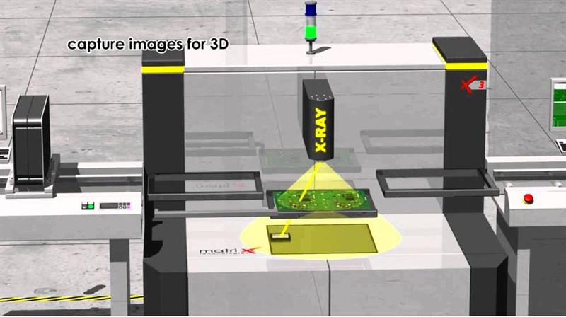
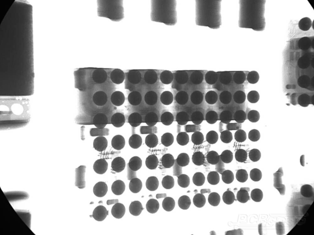
X-rays are high-energy electromagnetic radiation that can penetrate a component to analyze its internal structures such as contacts, displacement, solder bridges, and solder flow-ups. Materials made of lighter elements are more transparent to x-rays while those of heavier elements absorb more rays and are easily imaged.

When an x-ray inspection system is integrated into a production line, it usually takes about 30 seconds for it to check the components on a PCB. When the radiation passes through the component, different densities within the components attenuate different amounts of X-rays. For instance, board defects like porosity and incomplete welding will show as bright spots on the X-ray image while offsets caused by abnormal amounts of solder paste will show as unmatched shadows of the pin and the pad in the inspection image. 

The inspection image can also show you when a single BGA solder joint is not properly soldered or not as thick as it should be. The solder joint will appear brighter and look odd amongst the rest.


The x-ray inspection system can also help to:

  • perform a non-destructive inspection
  • locate short circuits on small footprint devices like BGA, CSP, QFN, and flip chip
  • detect voids in solder joints (BGA, CSP, QFN, QFP, and flip chip)
  • detect displacements of components
  • examine semiconductors (wire bonds, die alignment)
  • check switches, relays, and contacts
  • check plug, crimping, and cable connections (automotive)
  • perform a prototype inspection in order to avoid expensive production errors
  • optimize process parameters, and,
  • carry out random sample analyzes

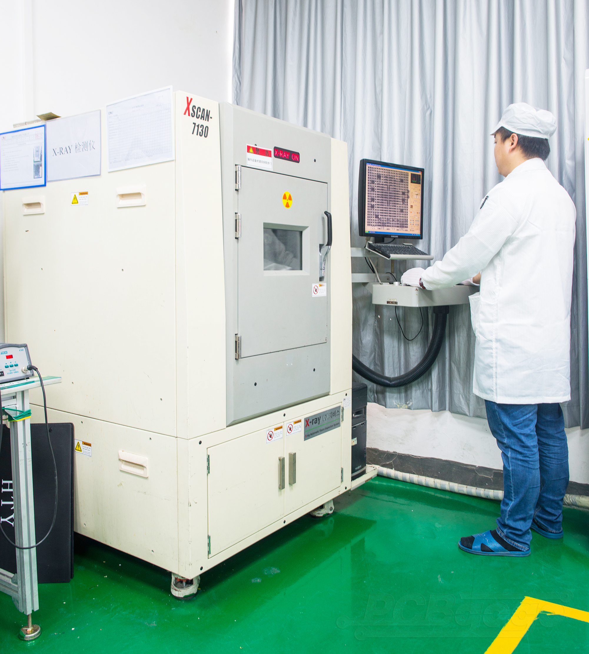
The X-ray inspection of PCBGOGO

For optimal use of the x-ray inspection system, it is important to have trained hands who can help to properly interpret the results from an x-ray inspection system and their relationship to process and component variables. Some defects can be detected easily while others can only be detected by their signatures which are known from experience. Skilled x-ray personnel like those at PCBGOGO make a difference in being able to help you screen for defective products based on your developed acceptance criteria for the defect.

The company provides a complete suite of PCB services, including PCB prototype, PCB assembly, PCB small-batch manufacturing, PCB testing, as well as an extensive line of Add-on services.

“We are proud of providing the best PCB manufacturing service at a competitive price. Our short lead time also can meet various requirements of customers from home and abroad”, they said.

If you would like to have an x-ray inspection done on your circuit boards, the company can test them and send a detailed report on the quality of the product. You can be sure to get the best of service from them.

Other useful details on the Automated X-ray Inspection system can also be found on their official website.

NXP Semiconductors PCF2131 Nano-Power Highly Accurate RTC

NXP Semiconductors PCF2131 Nano-Power Highly Accurate Real-Time Clock (RTC) features an integrated Temperature Compensated Crystal (Xtal) Oscillator (TCXO) and a 32.768kHz quartz crystal. The PCF2131 is optimized for very high accuracy and ultra-low power consumption. The PCF2131 offers a selectable I2C-bus or SPI-bus, a backup battery switch-over circuit, a programmable watchdog function, four timestamps function, and many other features.

The NXP PCF2131 Nano-Power Highly Accurate RTC has an operating temperature range from -40°C to +85°C in an HLSON 16 package.

Features

  • Operating temperature range from -40°C to +85°C
  • Temperature Compensated Crystal Oscillator (TCXO) with trimmed integrated capacitors
  • Ultra-low supply current of typical 64nA at VDD = 3.3V
  • Temperature-compensated RTC, typical accuracy ±3ppm from -40°C to +85°C
  • Integration of a 32.768kHz quartz crystal and oscillator in the same package
  • Provides year, month, day, weekday, hours, minutes, seconds, and 1/100 seconds
  • Provides leap year correction
  • Timestamp function
    • With interrupt capability
    • Detection of four different events on four input pins (for example, for tamper detection)
  • 2-line bidirectional 400kHz Fast-mode I2C-bus interface
  • 4-line SPI-bus with separate data input and output (maximum speed 6.5Mbit/s)
  • Battery backup input pin and switch-over circuitry
  • Battery backed output voltage
  • Battery low detection function
  • Power-On Reset (POR)
  • Power-On Reset Override (PORO) function
  • Software reset function
  • Two interrupt outputs (open-drain)
  • Programmable 1 second or 1-minute interrupt
  • Programmable watchdog timer with interrupt
  • Programmable alarm function with interrupt capability
  • Programmable square output
  • Clock operating voltage of 1.2V to 5.5V

more information: https://www.nxp.com/products/peripherals-and-logic/signal-chain/real-time-clocks/rtcs-with-temperature-compensation/nano-power-highly-accurate-rtc-with-integrated-quartz-crystal:PCF2131

Texas Instruments TCA9416 Ultra-Low Voltage I2C Translator

Texas Instruments TCA9416 Ultra-Low Voltage I2C Translator is a 2-bit bidirectional I2C, SMBus voltage-level translator with an output-enable (OE) input and rising and falling edge accelerators. It is operational from 1.08V to 3.6V on both the A-side and B-side. This feature allows the device to interface between lower and higher logic signal levels at any of the typical 1.2V, 1.8V, 2.5V, and 3.3V supply rails.

The OE input pin is referenced to VCCA, can be tied directly to VCCA, but it is also 3.6V tolerant. The OE pin can also be controlled and set to a logic low to place all the SCL and SDA pins in a high-impedance state, significantly reducing the quiescent current consumption. Under normal I2C and SMBus configurations, the TCA9416 is compatible with standard speeds where the frequency of SCL is 100kHz (Standard-mode), 400kHz (Fast-mode), or 1MHz (Fast-mode Plus).

The Texas Instruments TCA9416 features internal 10kΩ pull-up resistors on SCL_A, SDA_A, SCL_B, and SDA_B. Additional external pull-up resistors can be added to the bus to reduce the total pull-up resistance and speed up rising edges.

Features

  • 2-bit bidirectional translator for SDA and SCL lines in I2C applications
  • Provides bidirectional voltage translation with no direction pin
  • High-impedance output SCL_A, SDA_A, SCL_B, SDA_B pins when OE = 0V or VCC = 0V
  • Internal 10kΩ pull-up resistor on all SDA and SCL pins are enabled based on respective VCC voltage
  • 1.08V to 3.6V on both A and B ports
  • VCC isolation feature: If either VCC input is at GND, both ports are in the high-impedance state (excluding pull-ups)
  • No power-supply sequencing is required: either VCCA or VCCB can be ramped first
  • Low Ioff of 2.5µA when either VCCA or VCCB = 0V
  • OE input can be tied directly to VCCA or controlled by GPIO
  • Latch-up performance exceeds 100mA per JESD 78, class II
  • ESD Protection exceeds JESD 22
    • 2500V Human-body model (A114-B)
    • 1500V Charged-device model (C101)

more information: https://www.ti.com/product/TCA9416

ams NanEyeC Integrated Digital Camera Modules

ams OSRAM NanEyeC Integrated Digital Camera Modules are miniature-sized image sensors for vision applications where size is a critical factor. These modules are designed for the toughest confined space requirements with a small footprint of 1mm2 and 4 compact pads. The NanEyeC miniature camera modules from ams OSRAM achieve a frame rate of 0 to 58fps at 320 x 320 resolution with slave mode operation. These camera modules feature a highly sensitive 2.4-micron rolling shutter pixel and large full well capacitance. The sensor includes a 10-bit ADC and a bit-serial Single-Ended Interface Mode (SEIM) data interface that reduces external electronics for applications with short connections. An additional LVDS interface allows it to drive the signal for longer distances.

The NanEyeC miniature camera modules also feature 102.4kP resolution, 2.4µm x 2.4µm pixel size, and a rolling shutter type in a 2 x 2 SGA package. Combining a wide-angle view with a good depth of focus, the NanEyeC offers the speed and picture quality needed for an emerging set of video applications. These camera modules are ideally used in wearable devices, cameras, medical, and industrial applications.

Features

  • Designed for the toughest confined space requirements
  • Sharp and accurate image
  • Multi-element lens for optimal image quality
  • Footprint of 1mm2 with 4 contact pads
  • 2.4-micron high sensitive pixel with 102.4kp resolution
  • Frame rate of up to 58fps @ 320 x 320 resolution with slave mode operation
  • Digital interface
  • Cost-optimized
  • 2.4µm x 2.4µm pixel size
  • Rolling shutter type
  • High-end optics offering low distortion
  • Possible to switch the serial interface to a single-ended mode for easier connection to ISPs

Block Diagram

more information: https://ams.com/naneyec

Vishay / Sfernice P11H Modular High Torque Panel Potentiometers

Vishay / Sfernice P11H Modular High Torque Panel Potentiometers are designed to keep the setting under high mechanical constraints from vibration, shock, and other factors. Vishay / Sfernice P11H Potentiometers provide high torque (8Ncm) with a smooth feeling during the potentiometer’s entire life. The series offers 12.5mm2 single turn panel control with 6.35mm shaft diameters and operates over a lifespan of 50,000 cycles.

Features

  • Keep the setting under high mechanical constraints (vibration and shock)
  • High torque (8Ncm) with smooth feeling during all potentiometer life
  • Torque stability under high environmental constraints
  • 12.5mm2 single turn panel control with 6.35mm shaft diameters
  • Compact, versatile, modular, and robust
  • Tests according to CECC 41000 or IEC 60393-1

Specifications

  • IP64 sealing level
  • 50,000 cycles lifespan
  • Up to 7 modules

more information: https://www.vishay.com/potentiometers/list/product-51087/

Littelfuse CPC1596 Optically Isolated Load-Biased Gate Driver

Littelfuse, Inc. an industrial technology manufacturing company empowering a sustainable, connected, and safer world, announced the first high-voltage optically-isolated MOSFET gate driver on the market that requires no external power supply, yet can provide fast load turn-on speeds in the order of tens of microseconds. View the video.

The CPC1596 570V Optically Isolated Load-Biased Gate Driver is ideal for use in a wide range of power electronics applications including:

  • Industrial controls,
  • Automatic Test Equipment (ATE),
  • HVAC controls,
  • Medical devices,
  • Internet of Things.

“The CPC1596 570V Load-Biased Opto-Gate Driver addresses a critical market need,” said Steve Andrezyk, Senior Product Marketing Manager at Littelfuse. “Universal AC power line applications now have a custom, higher power optically isolated solid-state relay (SSR) solution without the cost of an auxiliary power supply or additional discrete devices to meet fast start-up speed requirements.”

The CPC1596 offers these key benefits:

  • Boosts external MOSFET start-up speed by using load-biasing.
  • Eliminates the need for an opto-gate driver auxiliary power supply.
  • Supports optically isolated SSR-applications for both AC and DC.
  • Enables using higher power MOSFETs.
  • Can be controlled from a logic port.

How it works

The problem: Standard Photovoltaic (PV) Gate Drivers simplify SSR-design by eliminating the need for auxiliary power supplies. Due to output currents in the µA-range, they get slower with larger gate charges of external MOSFETs, making it difficult to fulfill demanding fast turn-on application requirements.

The solution: The CPC1596 provides fast turn-on switch speed (typically 40µs) enabling designers to create a custom, higher power, optically isolated, DC-only or AC/DC solid-state relay (SSR) with external MOSFET(s). To increase the switching speed, simply utilize the product’s unique load-biasing, on-board circuit. The use of load-biasing eliminates the need for an opto-gate driver auxiliary power supply. An internal regulator circuit regulates the voltage drawn from the load supply (up to 570V) down to 12.2V for internal use. An external storage capacitor  is added to enable constant voltage control for properly driving the MOSFET.

Availability

The CPC1596 is provided in tape and reel format in quantities of 1,000. Sample requests can be placed through authorized Littelfuse distributors worldwide. For a listing of Littelfuse distributors, please visit Littelfuse.com.

For More Information

Additional information is available on the CPC1596 Optically Isolated, Load-Biased MOSFET Gate Driver product page. For technical questions, please contact: Anthony Konopka, Applications Engineer at  AKonopka@Littelfuse.com.

Bürklin Elektronik offers premium miniature fan units from Fischer Elektronik

Leading international distributor Bürklin Elektronik offers a premier range of miniature fan units to meet the increasing demands of small, high-performance electronic components. The LAM K series from Fischer Elektronik comprises miniature fan units to dissipate large amounts of heat in small spaces.

Electronic assemblies are becoming increasingly compact. Combined with high-performance components and high heat generation this can lead to considerable power losses, malfunctions, or even component destruction, without efficient thermal management. Miniature fan units, each with a fan motor, are available in 30×30, 40×40 and 50x50mm dimensions, each equipped with a double ball bearing system adapted to industrial requirements. They are extremely effective for cooling large power losses in small installation spaces.

For larger circuit board dimensions or higher power dissipation, miniature fan coil units are also available in 60.5×30, 80.8×40, and 100.5x50mm dimensions as a double version. The basic structure of these tube profiles consists of a circumferential rectangular base frame with a material thickness of 2.5 to 4.5mm. The respective outer surfaces of the frame with an opposing ribbed structure also serve as semiconductor mounting surfaces with a flatness of 0.1mm. This means they do not have to be additionally face-milled.

The Axial fan motors can be mounted quickly and easily in mounting holes integrated into the profile using screw mounting. A relatively high airflow rate at high dynamic pressure also ensures air transport over longer cooling distances or unit lengths. The technical quality parameter MTBF (Mean Time Between Failures), measured at an ambient temperature of 20°C, is up to 280,000 hours.

The fan motors offer voltages between 5V, 12V and 24V, according to the application. They can also be equipped with an additional pulse output to control an alarm generator circuit when the fan is selected or to monitor the rotor speed. The fan units can be installed directly on the printed circuit board and consist of a tubular aluminum profile with a special internal heat exchange structure.

Fan units can be mounted directly on the components concerned. The miniature fan units of the LAM K series offer two different mounting options for component attachment in conjunction with the matching spring geometry. The semiconductor assembly of the electronic components on the LAM K series can be carried out using several different methods, including classic screw mounting or with the aid of snap-in transistor retaining springs. The retaining springs, adapted for the designs of the LAM K series, can be quickly and easily snapped into the groove geometry of the base profile provided for component fastening.  The contact force achieved by the retaining springs provides an optimal thermal transition from the component to the cooling unit.

Irrespective of the chosen mounting method, the snap-in transistor retaining spring holds firmly in position. The high contact pressure achieved by the retaining spring fixes the transistor optimally on the mounting surface so that there is excellent heat transfer resistance between the component and the cooling element.

The Fischer Elektronik LAM K Series is available to order now from Bürklin Elektronik. Customers can rapidly locate and order through the search function at www.buerklin.com. Comprehensive product datasheets are also available online, with certifications and approvals available on request.

Meet the Newest and Easy-to-Use Move-Shoot-Move (MSM) Star Tracker

The new Move-Shoot-Move (MSM) Star Tracker is a device that can be used to capture clean and clear astro pictures. It is compact, easy to setup (in two minutes); and can do time-lapsed movements, 5-minute exposures with no trails, and Polar Alignment. This makes it capable of capturing excellent pictures; thanks to its compatibility with any camera type available, using the hot-shoe port or the intervalometer.

It is designed for wide-angle Astro-landscape, with a maximum 135mm focal length for best results, except the effect of torque has been carefully considered. The maximum lens length of 305mm (12 inches) allows for better capturing and expression.

With a seamless mechanism of operation, the MSM defies the 500 rule and allows exposure of more than 60 seconds, using polar alignment. The 500 rule limits exposure time to 25s, maximum. Longer time exposures result in ugly star trails, noise, and the missing of many faint stars in the photo.

MSM star tracker beats the odds because it rotates at the same speed as the Earth, but in the opposite direction. This means that the stars can be tracked and remain in the viewfinder, an exposure time up to minutes in duration is possible, faint stars are visible, star trails disappear, and lower ISO helps to reduce noise. So you see, clear, pinpoint photos of stars and the night sky can be taken easily due to its unparalleled working mechanism.

The 1.7″ x 3.15″ x 3.9″ (4.3cm x 8cm x 9.9cm) MSM works by adjusting the angle of rotation and not the speed of rotation, making four options available for use: Star Tracking Mode, Move Shoot Move mode of 0.05, 0.075, 0.1, and 0.125 degrees per picture. The camera’s rotation can be controlled based upon the angle selected, and the interval set on the timer (A separate timer/intervalometer is needed for time-lapse shots).

The longer the interval set, the slower the rotation. Once a picture has been taken (this is made obvious to the rotator by the hot-shoe cable), the rotator turns the defined angle. This invariably means the camera will not turn while the picture is being taken.

The MSM star tracker also sports an innovative worm gear system that presents two key benefits: Top-Level Move Shoot Move performance and Super Long Battery Life. Amazing!

With the new button model of this beauty, we now have a sturdy device that has a button 15% smaller than the knob, an added 1/2 speed star tracking mode (which makes taking photos of the Milkyway in one shot possible), no panorama mode due to the small frequency of its use, and an illuminator added to the polar scope. It is also easier to install with the new stopper screws.

What’s more? The MSM is made with Aluminium alloy, has a 450g weight, a maximum 3kg load, Star Tracking Mode (360° in 24hrs) | 0.05°/step, 0.075°/step, 0.1°/step, 0.125°/step, DC 5.0V 1.0A Max input, battery life of 5hrs for star tracking or 3000 shots for time-lapse, and a 1 year warranty period.

You can place your order for the various MSM star tracker options on their official website, here:  https://www.moveshootmove.com/collections/sifo-rotator/products/sifo-rotator-for-star-tracking-time-lapse-panorama-photography?aff=13

Elkhart Lake Processors Power Thin Mini-ITX motherboards for IoT applications

Elkhart Lake Processors

To support the next generation of IoT edge devices, Intel has developed a new line of processors enhanced for IoT. In comparison to 14nm generation processors, the new Elkhart Lake processor offers up to 1.7x better single thread, 1.5x better multi-thread, and 2x better graphic performance thanks to 10nm SuperFin fabrication technology. These next-generation solutions offer real-time performance, flexibility, and a slew of Intel technologies to power edge computing.

With the release of these Intel Elkhart Lake processors, many third-party manufacturers have come up with hardware based on this chip, such as MiTac’s PD10EHI, DFI’s EHL171/EHL173, and ASRock’s IMB-1004 thin Mini-ITX boards. Mini-ITX offers the optimal blend of functionality and performance with its extensive I/O ports and interfaces that can quickly fulfill diverse applications required by a wide range of industries. Thus, they provide an ideal solution for AGV/AMR, KIOSK, digital signage, and gaming.

MiTac’s PD10EHI Elkhart Lake Processor thin mini-ITX motherboard

MiTac, a global pioneer in industrial computing and an Intel Titanium Partner, has developed the PD10EHI, a high-performance, low-power Elkhart Lake industrial motherboard.

With the Intel Programmable Services Engine, the PD10EHI takes advantage of a dedicated offload engine. It is powered by an ArmCortex-M7 microcontroller and offers independent, low-DMIPs computing as well as low-speed I/Os for IoT applications. It also includes additional features such as remote, out-of-band device administration, network proxy, embedded controller, and sensor hub.

MiTac’s PD10EHI Elkhart Lake thin mini-ITX motherboard

The quad-core Atom x6413E / Celeron J6413 processor is clocked at 1.5GHz / 1.8GHz with 3.0GHz Turbo Burst for the high-end SKUs of the board. Intel UHD Graphics are also included, which support up to 16EU (Execution Units) of graphic processing capability. The PD10EHI has two DDR4 SO-DIMM sockets, allowing it to use up to 32GB of non-ECC memory with a 3200 MHz maximum clock frequency.

For storage installation, it also has two SATAIII ports which are multiplexed with M.2 and mSATA connections. Internal slots include PCIe Gen3 for add-on cards, sufficient storage, or LTE/5G expansion through M.2 B key 2280/2260/2242/3052/3042 and E key 2230 for WiFi/Bluetooth. It also has 1x mini PCIe and a maximum of 6 COM ports for expansion to maintain flexibility in multiple applications.

Block Diagram of PD10EHI

Block Diagram of PD10EHI

In addition, the integrated 10th generation Intel HD graphics unit supports Triple Display at a maximum resolution of 4K. An HDMI port with a resolution of up to 4096×2160 pixels, a display port with a maximum of 4096×2160 pixels, and an LVDS port with a Full HD 1920×1200 pixel resolution is available for connecting displays. The LVDS port can be replaced with an eDP port with a resolution of 4096×2160 pixels. Hence, it is ideal for multimedia applications like Kiosk, Signage, or Factory automation like HMI.

The MiAPI pin header additionally features 10 GPIOs, a watchdog, SMBUS, UART, and mainboard monitoring functionality. The PD10EHI can operate in a voltage range of 8 to 24 volts DC and temperatures ranging from 0 to 60 °C. The wide voltage power input makes this motherboard ideal for industrial embedded systems with longevity, stability, and reliability.

DFI’s EHL171/EHL173 Motherboard

DFI’s EHL171-EHL173 motherboard

DFI’s EHL171/EHL173 is the only model that includes one of the 10nm-fabricated Elkhart Lake’s “FE” variants. Thus, it provides Intel Safety Island technology with functional safety (FuSa). DFI’s embedded industrial motherboards with a high-class lifespan deliver value-added services to a wide range of embedded applications based on cutting-edge platforms and technologies.

In addition to the quad-core Atom x6427FE with a clock speed of up to 1.9GHz, there is a quad-core 2GHz/3GHz Atom x6425E and a quad-core Pentium J6413. Dual slots support up to 32GB DDR4-3200 memory, and the board also includes two 2.5GbE ports. The board comes with two M.2 slots (B- and E-key), a nano-SIM socket, and PCIe x4 support (PCIe x2 signal).

It can support up to 4K resolution and has a triple display. This includes eDP/LVDS as well as HDMI and DP++ ports. Onboard there are 2x USB 3.1 Gen2 ports, 2x USB 3.1 Gen1 ports and 6x USB 2.0 headers. It additionally provides GPIO or DIO, a watchdog, and a TPM option. The manufacturer also offers an LCD inverter connector.

Block Diagram of DFI’s motherboard

DFI is the only board that can withstand temperatures ranging from -40 to 85°C. Except for the Pentium J6413 SKU, which supports -5 to 65°C, this is standard. The main difference between the EHL171 and the EHL173 is that the EHL173 has a 9-36V input instead of 12V. Only two of the three EHL173 models have a 9-36V input: the Atom x6425E and the J6413.

ASROCK’s IMB-1004

ASRock Industrial’s Mini-ITX motherboards powered by Elkhart Lake processors are the most popular form factor (6.7-inx 6.7-in) with extensive I/O expansion and good performance. ASRock doesn’t have any Atom models, although it does have dual-core and quad-core Celeron and Pentium chips.

ASROCK’s IMB-1004 powered by Elkhart Lake Processors

The IMB-1004 also supports up to 32GB DDR4 memory with a 3200Mhz clock frequency. It features two SATAIII connectors, 2.5GbE and 1GbE ports. Furthermore, it includes three M.2 slots (M-, B-, and E-key), as well as a SIM card slot and a PCIe x1 interface.

Like PD10EHI and EHL171/EHL173, the IMB-1004 also offers triple-independent displays. HDMI, VGA, eDP/LVDS, and a speaker header are all provided by the firm. Additionally the board includes 2x USB 3.2 Gen1 and 2x USB 2.0 ports, as well as 2x Gen1 and 6x USB 2.0 internal headers. Similarly, this board also supplies GPIO or DIO, a watchdog, and a TPM option.

Discussing further, the DFI’s EHL171/EHL173 is compatible with both Linux and Windows 10 IoT Enterprise. While the PD10EHI from MiTac supports Windows 10, and Linux is only available on request. ASRock Industrial does not specify an operating system. However, unlike ASRock’s Windows-oriented commercial unit, ASRock Industrial usually supports Linux.

MiTac’s PD10EHI is available from ICP Germany, which does not list pricing; however, ChirpLabs sells it for $300 with a Pentium N6415. DFI’s EHL171/EHL173 and ASRock Industrial’s IMB-1004 have no pricing or availability information at this point in time.

Via LinuxGizmos

Small, high-brightness RGB LEDs boast improved color mixing

Upward-lighting multicolor LEDs in the CL-V501 Series from Citizen Electronics have improved color mixing, come in a small package, and exhibit high brightness. Multicolor LEDs have three dies of RGB (red, green and blue) in one package. This lets them generate various colors, including white, and are used for illumination or as indicators in many kinds of products such as digital devices. In recent years, applications for illumination in-game devices, keyboards for personal computers and amusement devices have been expanding. The number of devices that contain a lens and light guide to create a complicated lighting expression has increased. With this background, smaller, high-brightness LEDs are required, and good color mixing properties when more than two dies are lighted simultaneously is an important factor so as not to damage the design and functionality of the device.

Through our unique packaging technology based on high-density packaging, we have realized a high color mixing property that conventional packages were unable to achieve. Downsizing and high-brightness are also achieved enabling customers to use a wide variety of expressions they require.

Main LED characteristics include:

  • Natural white color realized by high color mixing property. White color generated by lighting RGB dies in conventional multicolor LEDs had poor color mixing. Thus, in some cases, a RGBW LED was used in which a white (W) LED is added to an RGB device. This solution makes the LED package larger and circuit design of the device complicated and was expensive. However, by developing the composition of raw materials and adopting a new manufacturing method, we have succeeded in controlling directivity in the device itself. The natural white color is realized with this high color mixing property. As the light source does not generate color breakup, the design is improved. Even in cases where a lens and light guide plate are used, it is easier for developers to create designs because the light source itself has color mixing.
  • Both high-brightness and small size are realized, and luminous efficacy per unit area is doubled. We have further developed our high-density packaging technology to achieve a small package with good color mixing properties. Compared with our conventional product, the area of the LED is reduced by 30%, and luminous area is reduced by 50%.

This downsizing contributes to space-saving of the mounting area of the device, and the doubling in luminous efficacy per unit area can reduce energy consumption.

The CL-V501 dimensions are 1.6×1.4 mm. Mounting area is 2.24 mm (Luminous area is 1.34).

Applications include illumination and indicators for game devices, keyboards for personal computers, home appliances, hobby goods, displays, ambient lighting for automobiles, and colored lighting. Mass production begins in January 2022.

Citizen Electronics Co., Ltd., https://ce.citizen.co.jp/e/

TOP PCB Companies