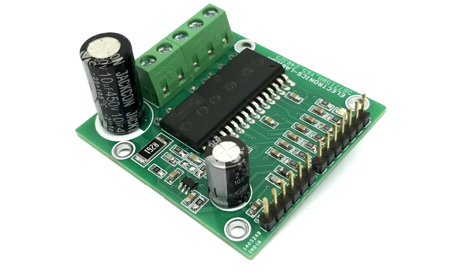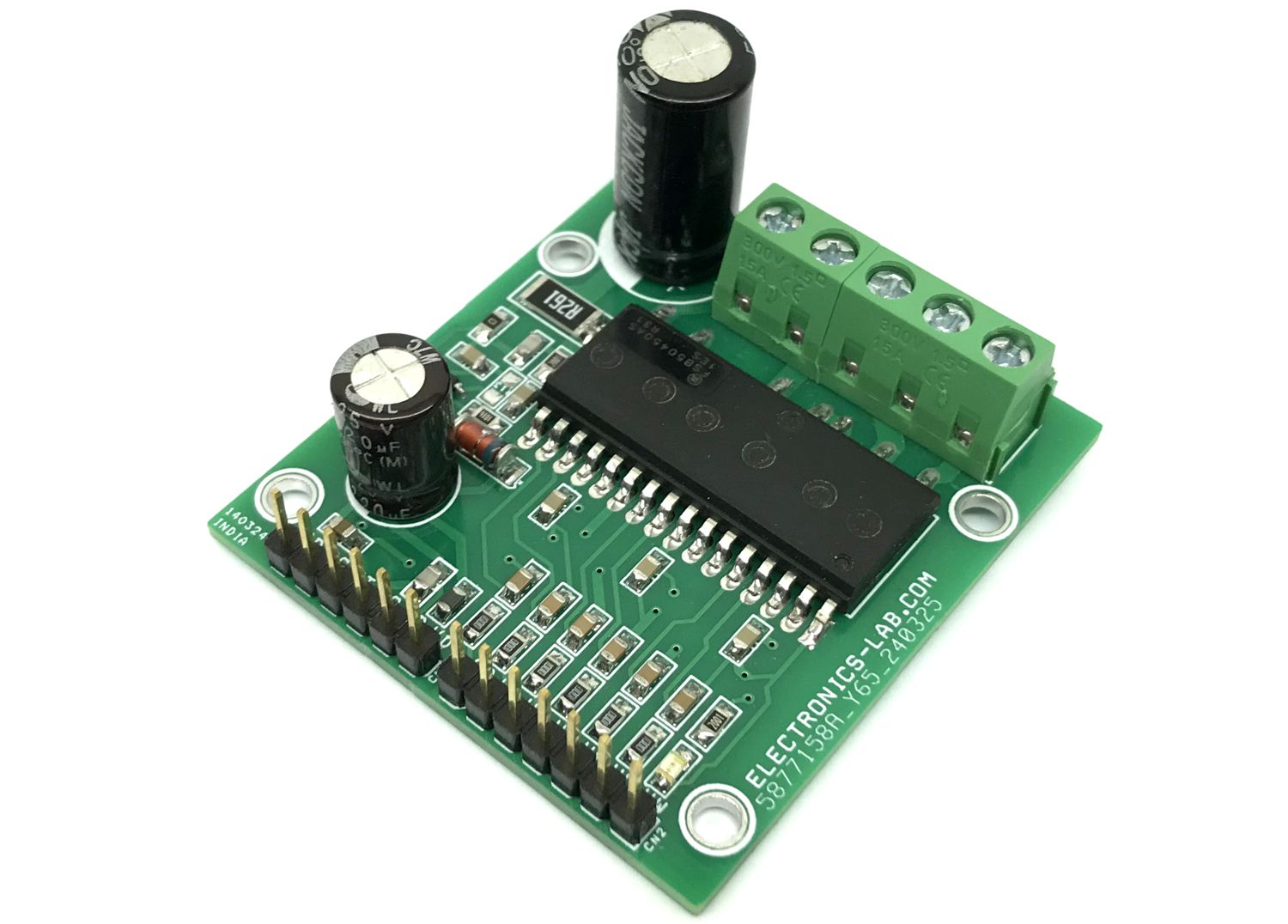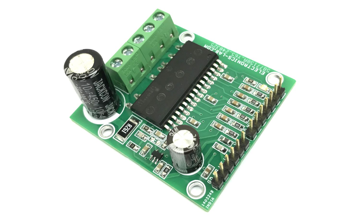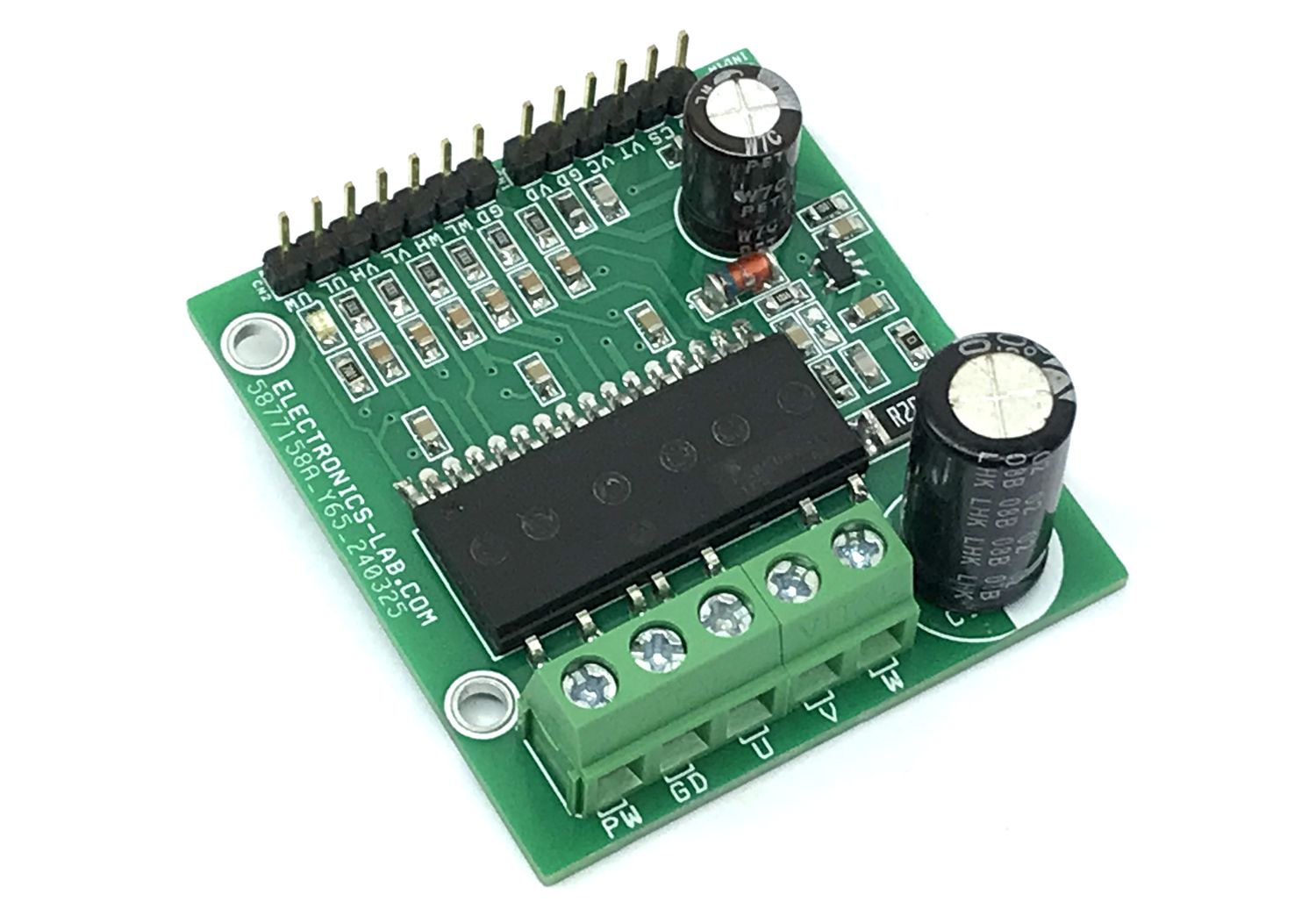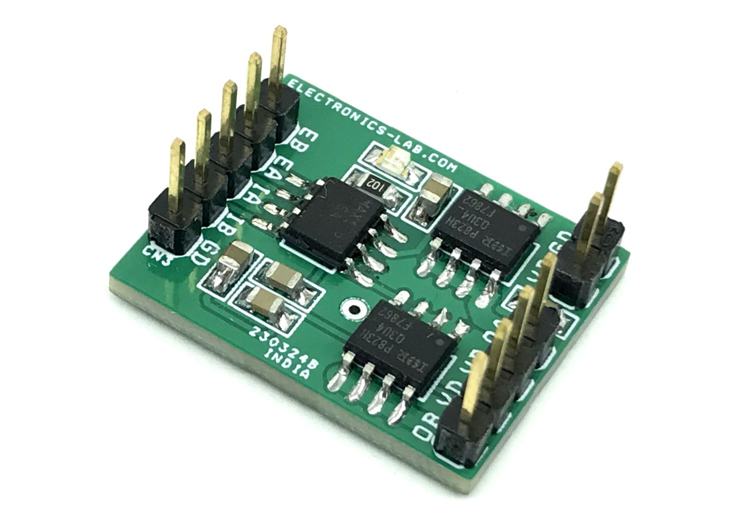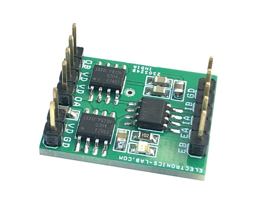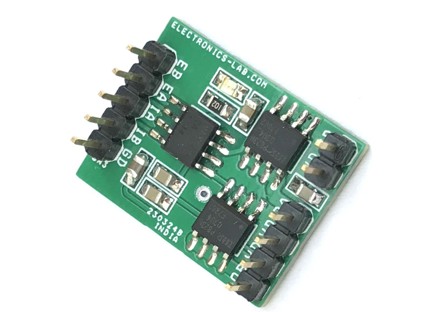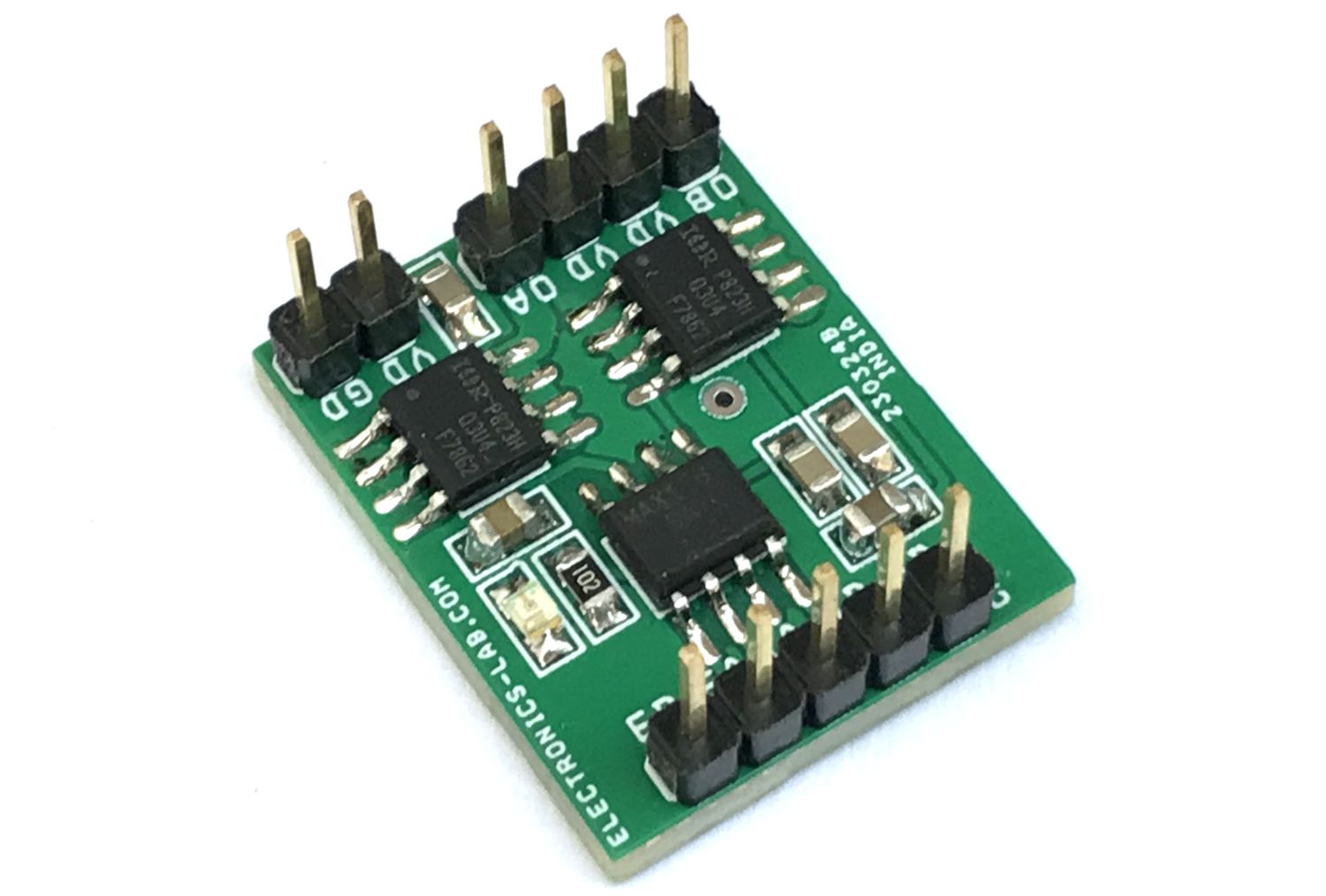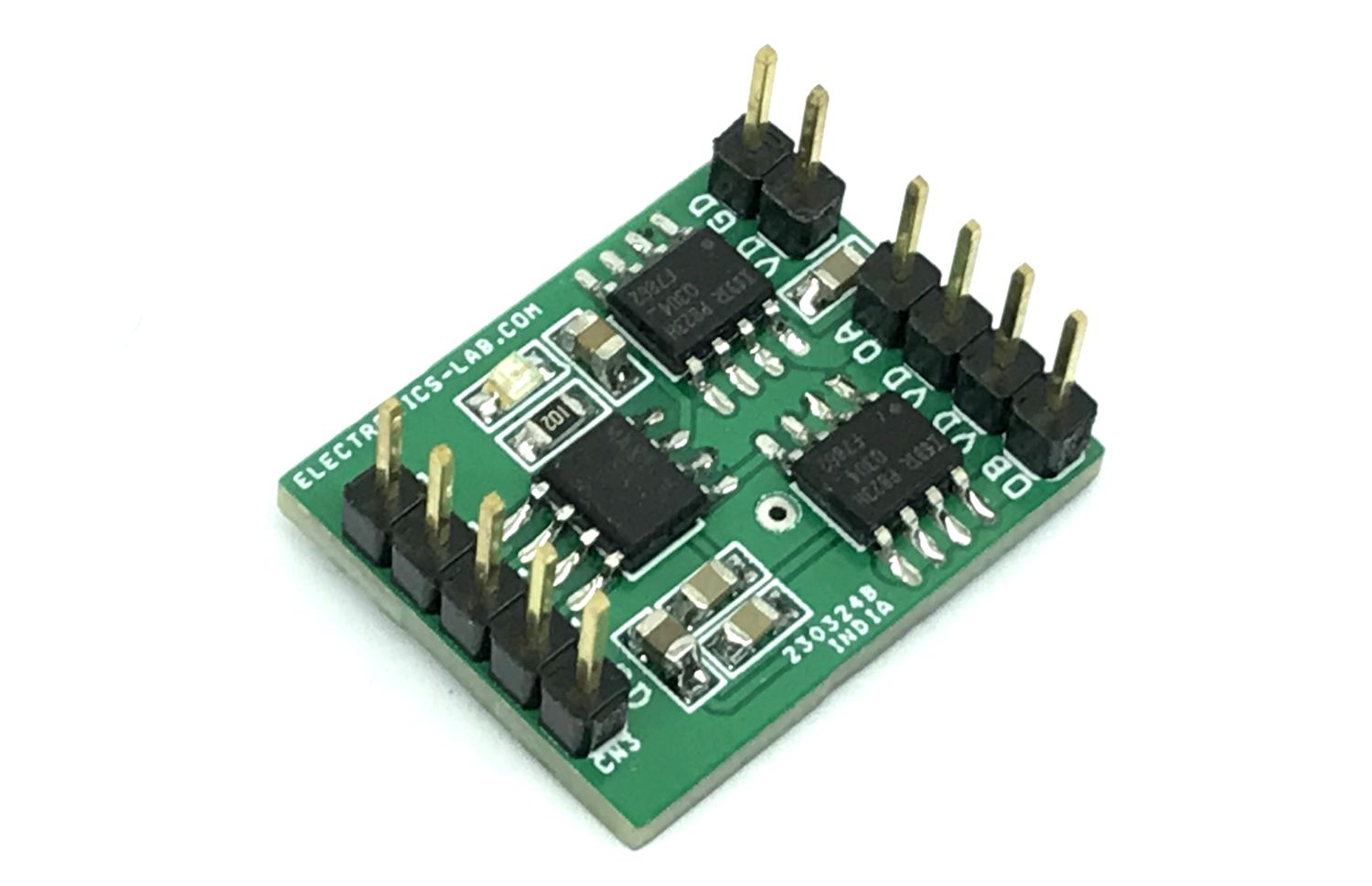
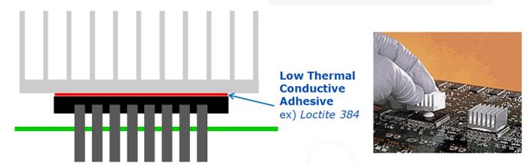
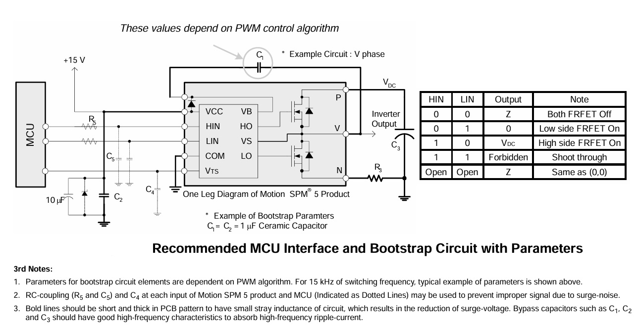
This is a 3-Phase Inverter Driver project designed for Low Power AC Motor. The FSB50450AS chip is the heart of the project. A compact inverter project is ideal for small power motors such as fans and pumps. An H-bridge configuration can also be created for low-current high-voltage brushed DC motors. The Inverter project supports loads up to 1.5A. The DC power supply voltage is up to 400V DC. The project operates with 6 x PWM signals. Parameters for bootstrap circuit elements are dependent on the PWM algorithm. For 15 kHz switching frequency, Bootstrap capacitors C1, C2, and C3 value is 1uF. Resistor R1, R2, R3, R4, R6, R7 and capacitor C4, C5, C6, C7, C8, C9 prevent improper signal due to surge-noise. Over-current or fault detection circuit is created using comparator CN5 – LMV7239 and shunt resistor R5. The output of LMV7239 is normally high and goes low when an over-current condition occurs. So, the CS pin goes low when the current goes above the threshold level. ATS pin is provided to monitor the temperature of the IPM chip. Heatsink is a must for this IPM module. Adhesive material with high thermal conductivity, such as Loctite 384, can be used to fix the heat sink on the top surface of the chip. Refer to the heatsink installation diagram.
Operation Truth Table
- HIN 0, LIN 0 = Output Z Both MOSFET Off
- HIN 0, LIN 1 = Output 0 Low Side MOSFET On
- HIN 1, LIN 0 = Output VDC High Side MOSFET On
- HIN 1, LIN 1 = Forbidden Shoot Through
Features
- Load Power Supply Up to 400V DC
- Load Current Continues 1.5A
- Logic Supply 15V DC
- Power Supply for Over Current Circuit (Comparator CN5) 5V DC
- One Board Power LED for Logic Supply
- Shunt Based Over Current Output
- VTS Pin for Temperature Monitor (Temperature sensing built in HVIC)
- HVIC for gate driving and under-voltage protection
- Active-High interface, can work with 3.3V/5V logic (PWM Signals)
- Optimized for low electromagnetic interference
- Isolation voltage rating of 1500Vrms for 1min
- PCB Dimensions 50.17 x 45.72 mm
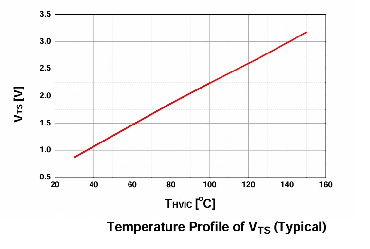
Temperature Sensing Output (VTS) – CN1 Pin 4-VTS
Pin: VTS This indicates the temperature of the V-phase HVIC with analog voltage. HVIC itself creates some power loss, but mainly heat generated from the MOSFETs increases the temperature of the HVIC. This Pin provides voltage output when the temperature rises, this pin can be interfaced with the ADC of the MCU to monitor the temperature. Refer to the Temperature vs VTS output diagram for more information.
Signal Input Pins
- Pins: IN(UL), IN(VL), IN(WL), IN(UH), IN(VH), IN(WH)
- These pins control the operation of the MOSFETs.
- These pins are activated by voltage input signals. The terminals are internally connected to the Schmitt trigger circuit.
- The signal logic of these pins is active HIGH; the MOSFET turns ON when sufficient logic voltage is applied to the associated input pin.
- The wiring of each input needs to be short to protect the module against noise influences.
- An RC filter is used to mitigate signal oscillations or any noise that traces of input signals may pick up.
Minimum Pulse Width (Signal Input)
There are input noise filters of 90 ns time constant inside the HVIC. It screens out pulses narrower than the filter time constant. Additional propagation delay in level-shifters and other circuits, together with gate charging time, prevent SPM 5 products from responding to an input pulse narrower than ~120 ns. Gate signal inputs are active-HIGH with 500 kΩ internal pull-down resistors.
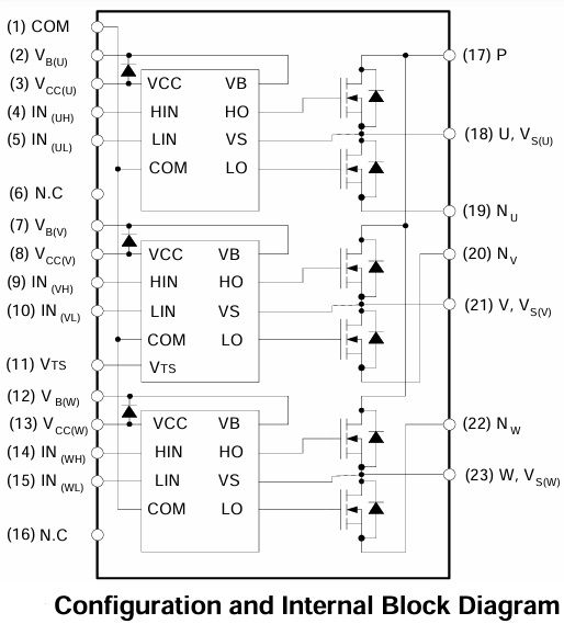
FSB50450AS is an advanced Motion SPM® 5 series based on fast-recovery MOSFET (FRFET®) technology as a compact inverter solution for small power motor drive applications such as fans and pumps. FSB50450AS contains six FRFET MOSFETs, three half-bridge gate driver HVICs with temperature sensing, and three bootstrap diodes in a compact package fully isolated and optimized for thermal performance. FSB50450AS features low electromagnetic interference (EMI) characteristics through optimizing switching speed and reducing parasitic inductance. Since FSB50450AS employs MOSFETs as power switches, it provides much more ruggedness and larger safe operating area (SOA) than IGBT-based power modules. FSB50450AS is the right solution for compact and reliable inverter designs where the assembly space is constrained.
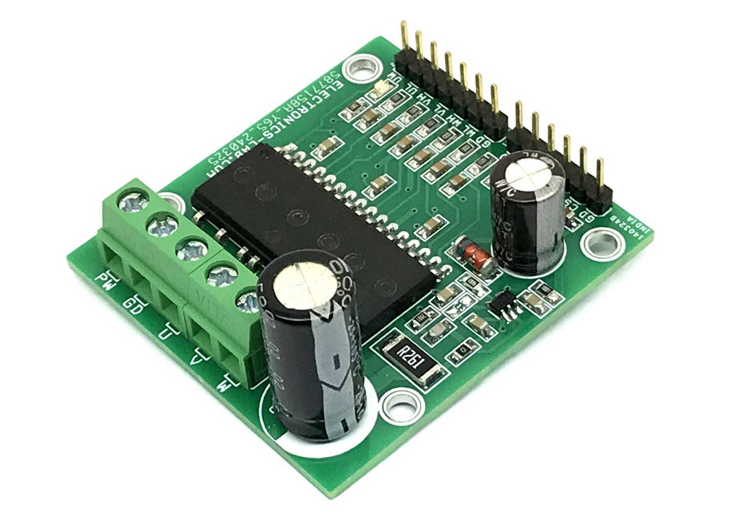
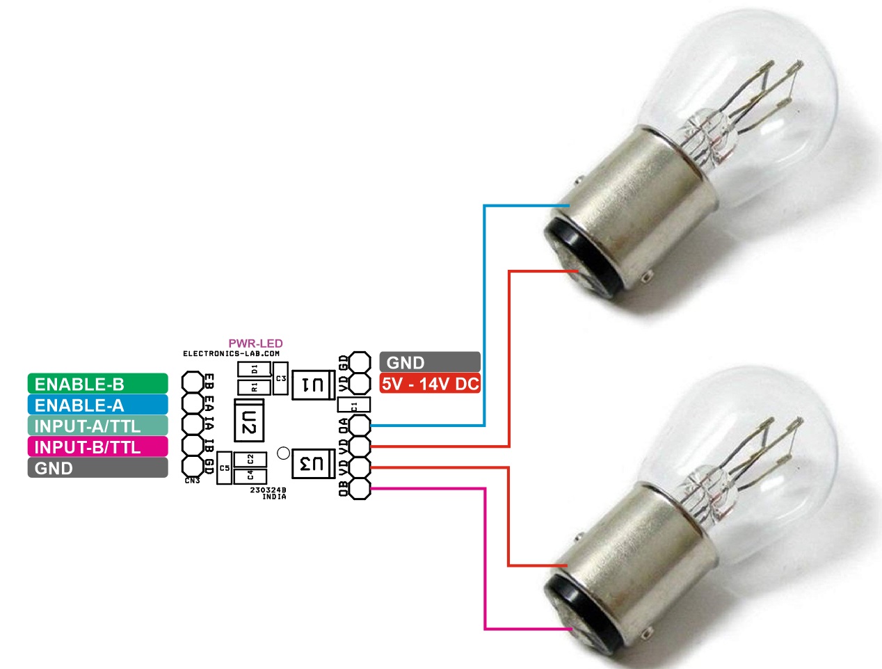
Connections
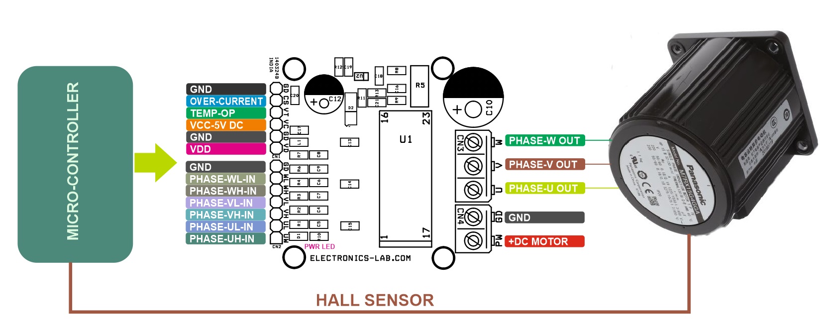
- CN1: Pin 1 VDD 12V to 15V DC, Pin 2 GND, Pin 3 = VCC 5V DC, Pin 4 = VTS/Temperature NTC, Pin 5 = Over Current/Fault Output, Pin 6 = GND
- CN2: Pin 1 = PWM U-High, Pin 2 = PWM U-Low, Pin 3 = PWM V-High, Pin 4 = PWM V-Low, Pin 5 = PWM W-High, Pin 6 = PWM W-Low, Pin 7 = GND
- CN3: 3 Phase Motor, Pin 1 = Phase=W, Pin 2 = Phase-V, Pin 3 = Phase-U
- CN4: Pin 1 = Motor Supply 400V DC, Pin 2 = GND
- D1: Power LED for Logic Supply
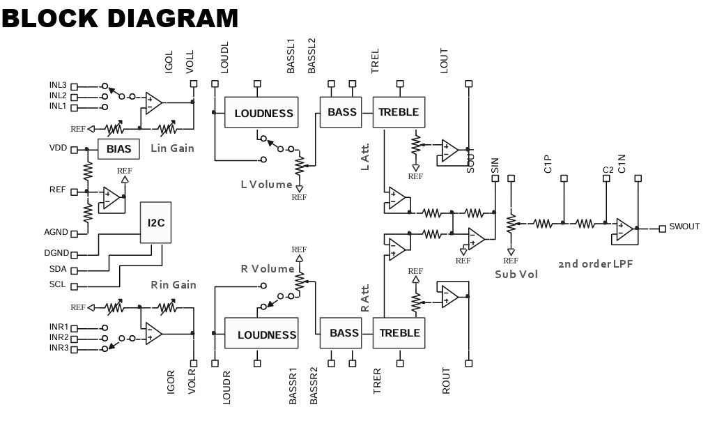
Block Diagram
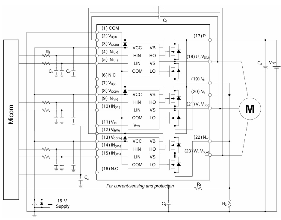
Typical Application
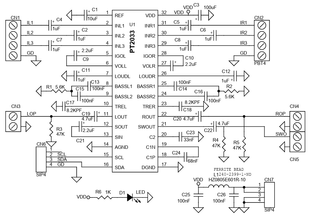
Schematic
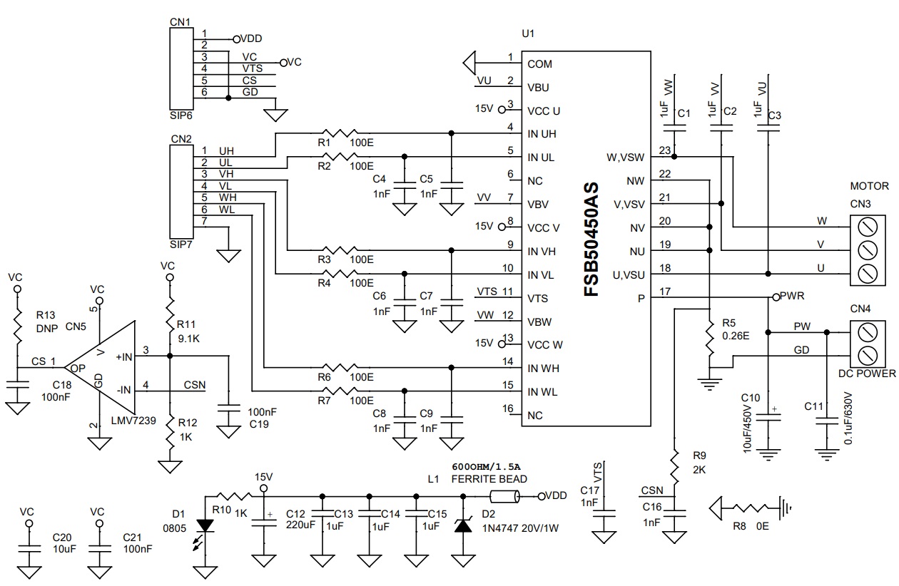
Parts List
| NO. | QNTY. | REF. | DESC. | MANUFACTURER | SUPPLIER | SUPPLIER PART NO |
|---|---|---|---|---|---|---|
| 1 | 1 | CN1 | 6 PIN MALE HEADER PITCH 2.54MM | WURTH | 732-5319-ND | |
| 2 | 1 | CN2 | 7 PIN MALE HEADER PITCH 2.54MM | WURTH | 732-5320-ND | |
| 3 | 1 | CN3 | 3 PIN SCREW TERMINAL PITCH 5.08MM | PHOENIX | 277-1248-ND | |
| 4 | 1 | CN4 | 2 PIN SCREW TERMINAL PITCH 5.08MM | PHOENIX | 277-1247-ND | |
| 5 | 1 | CN5 | LMV7239 SOT23-5 | TI | LMV7239M5X/NOPBCT-ND | |
| 6 | 3 | C1,C2,C3 | 1uF/35V CERAMIC SMD SIZE 1206 | YAGEO/MURATA | ||
| 7 | 8 | C4,C5,C6,C7,C8,C9,C16,C17 | 1nF/50V CERAMIC SMD SIZE 0805 | YAGEO/MURATA | ||
| 8 | 1 | C10 | 10uF/450V ELECTROLYTIC 12.5MM DIA | PANASONIC | P13558-ND | |
| 9 | 1 | C11 | 0.1uF/630V CERAMIC SMD SIZE 2220 | TDK | 445-13136-1-ND | |
| 10 | 1 | C12 | 220uF/25V ELECTROLYTIC | PANASONIC | P10271-ND | |
| 11 | 3 | C18,C19,C21 | 100nF/50V CERAMIC SMD SIZE 0805 | YAGEO/MURATA | ||
| 12 | 1 | D1 | LED RED SMD SIZE 0805 | OSRAM | 475-1278-1-ND | |
| 13 | 1 | D2 | 1N4747 1W 20V ZENER | MICROCHIP | 150-1N4747UR-1/TRCT-ND | |
| 14 | 1 | L1 | FERRITE BEAD 600OHM/1.5A SMD SIZE 0805 | LAIRD | ||
| 15 | 6 | R1,R2,R3,R4,R6,R7 | 100E 5% SMD SIZE 0805 | YAGEO/MURATA | ||
| 16 | 1 | R5 | 0.26E/2W 1% SMD SIZE 2512 | YAGEO/MURATA | 13-PT2512FK-7W0R26L-ND | |
| 17 | 1 | R8 | 0E SMD SIZE 0805 | YAGEO/MURATA | ||
| 18 | 1 | R9 | 2K 1% SMD SIZE 0805 | YAGEO/MURATA | ||
| 19 | 2 | R10,R12 | 1K 1% SMD SIZE 0805 | YAGEO/MURATA | ||
| 20 | 1 | R11 | 9.1K 1% SMD SIZE 0805 | YAGEO/MURATA | ||
| 21 | 1 | R13 | DNP | |||
| 22 | 1 | U1 | FSB50450AS | ON SEMI | FSB50450ASCT-ND | |
| 23 | 1 | C20 | 10uF/25V CERAMIC SMD SIZE 0805 | YAGEO/MURATA | ||
| 24 | 3 | C13, C14,C15 | 1uf/25V CERAMIC SMD SIZE 0805 | YAGEO/MURATA |
Connections
Heatsink Installation
Microcontroller Interface
Gerber View
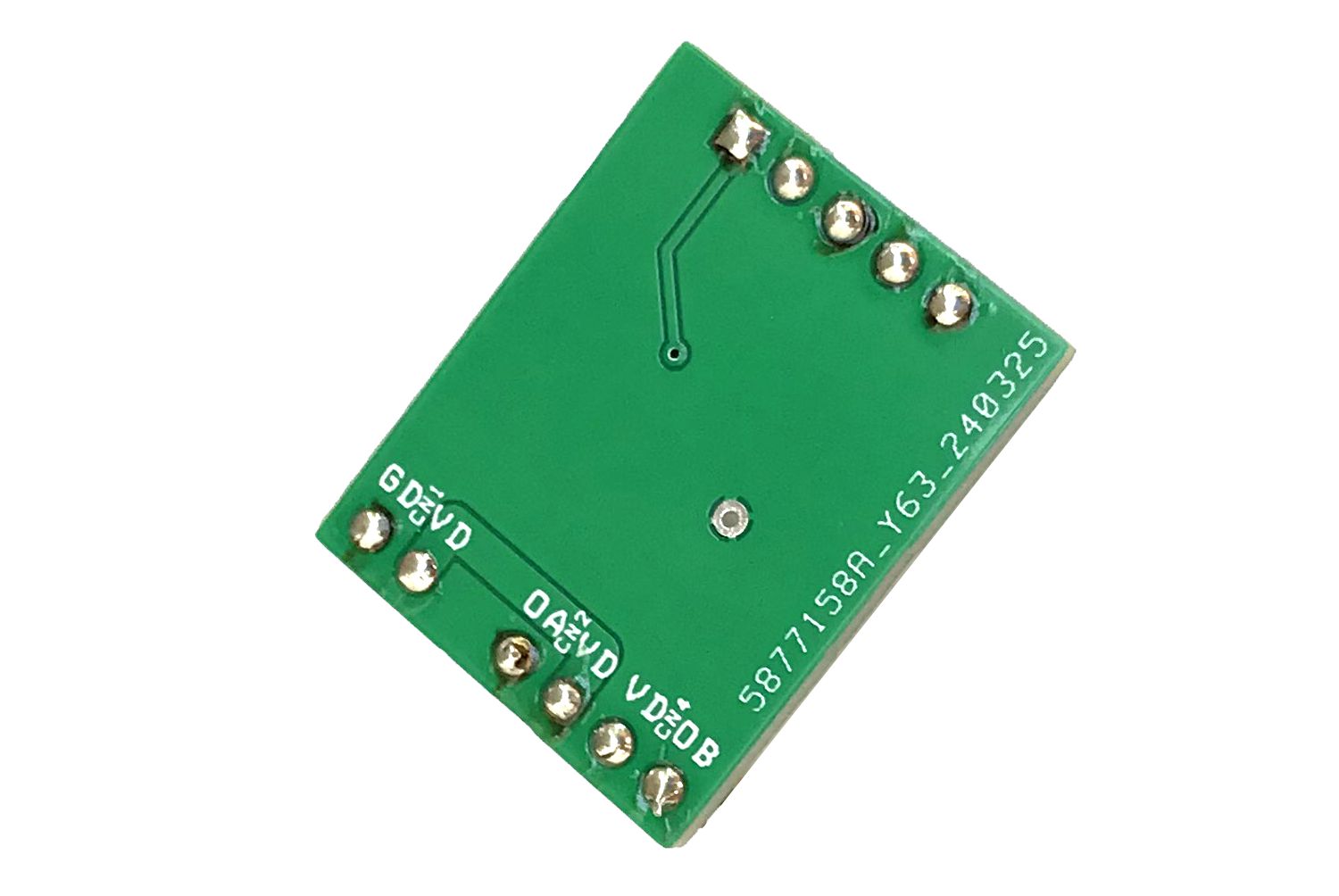
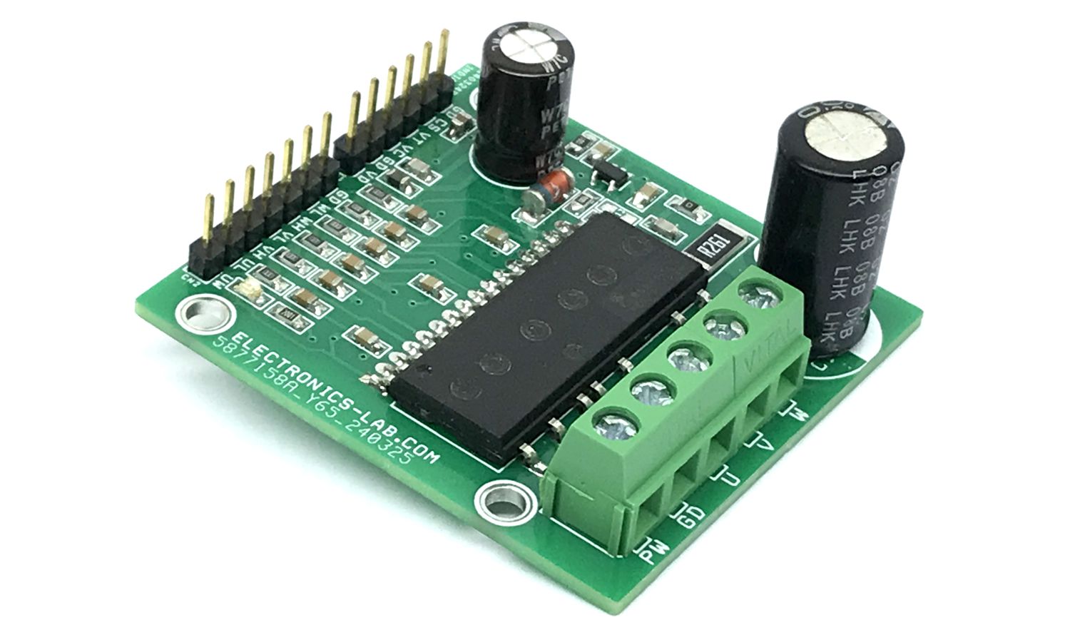
Photos